2017 2nd International Conference on Wireless Communication and Network Engineering (WCNE 2017) ISBN: 978-1-60595-531-5
Design and Implementation of Power Protection
Based on Single-chip Microcomputer
Yuan SUN
School of information Beijing Wuzi University Beijing, China
Keywords: MCU, Power drop, Loss of storage data, Procedures.
Abstract. The protection of instantaneous loss of storage data is an important function of industrial or civil equipment The data of MCU is in RAM memory, therefore data in RAM is unreserveable after losing power. After the power drop, the data in MCU is saved to the EEPROM memory in time. This method is a good solution to the data of MCU after power loss. The principles and methods and procedures are given in this paper.
Introduction of System
Loss of storage data is an important function of industrial or civilian equipment, for example, the production line of automatic production counting, switch life detection instrument and so on. These are all records of temporary data, some of which can't even appear to be missed, and are not allowed to lose all data due to sudden power outages. The data of microcomputer is present in RAM (random memory). The data in RAM is not retained after losing power, so how to make the data not lost after losing power? This requires an EEPROM or FLASHROM memory. In the microcomputer system, it is generally used to extend the memory, microcomputer and memory interface through I2C or SPI to communicate data. In the field of measurement and control, the data in the internal and external RAM of the microcomputer is often required, and the data in RAM can be kept when the power is lost.
Instruction of Chip Pin
[image:1.612.80.537.527.598.2]The serial EEPROM of AT24C series has the function of I2C bus interface. The power supply voltage is 2.5 ~ 2.6V and the current is about 3mA. It has many models, large capacity and I/O port is not used for microcomputer .Chip extended convenience and can be read and written easily. According to different models, the storage capacity is shown in table 1.
Table 1. AT24C serial EEPROM parameters.
model Capacity/B Number of bytes in a load (page write) AT24C01 128×8 4
AT24C02 256×8 8 AT24C04 512×8 16 AT24C08 1024×8 16 AT24C16 2048×8 16
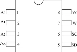
The AT24CXX series has many kinds of encapsulation, with the example of 8-pin, the chip pin drawing is shown in figure 1.
1
2
3
4 5
6 7 8 A0
A1
A2
VSS
VCC
WP
SCL
SDA
[image:1.612.238.370.623.712.2]The pin function is as follows:
SDA: serial data input/output terminal, serial two-way data input/output line SCL: serial clock terminal, which is used to synchronize input and output data. WP: write protection, this pin is used for hardware data protection.
A0~A2: chip selection or page selection address input. VCC: power supply
VSS: grounding
24C16 Read and Write Operation
Read Operation. The reading operation is divided into three types: (1)Read the data of the current address storage unit;(2) Read the data of the specified address storage unit; (3)Read the data of the continuous address storage unit
Read the data of the current address storage unit. The internal data store address counter of E2PROM records the operation address, which is the address of the last cell to be accessed in the last read or write operation. If the chip constantly, the address has been effective in the operation, when the MCU read data, back to the response signal and E2PROM chips was introduced, the current address points to storage unit is a serial data output.
Read the data of the specified address storage unit. MCU signal began to read data, and then send the read/write control word, the MCU send address to read data in E2PROM chips was introduced, if E2PROM chips was introduced to track the response signal, and record the current address of the storage unit. The MCU sends the start signal, sends the chip address and the read-write control signal, and then outputs the data sequentially if the E2PROM sends the reply signal. After reading the data, the microcomputer sends back the non-reply signal and a stop signal. In the controller program, the random byte program in 24C16 is put into an R24C16 subroutine, and the R24C16 subroutine is called whenever the data of 24C16 is read in the 89C52 MCU.
; subroutine of random bytes read 24C16 R24C16: NOP
RSTART: CLR ESCL NOP NOP
SETB ESDA NOP
SETB ESCL ; Open the START NOP
CLR ESDA NOP CLR ESCL ; Write 8 control words 1#
MOV A, #10100010B ;DEVICE ADDRESS MOV R7, #08H
READ1: RLC A
MOV ESDA, C ; A7 NOP
SETB ESCL NOP
CLR ESCL NOP
DJNZ R7, READ1
SETB ESCL ;ACK FROM 24C16 NOP
NOP ; Write 8-bit addresses
MOV R7, #08H ;ADDRESS MOV A, RDATAADR
READ2: RLC A
MOV ESDA, C NOP
SETB ESCL NOP
CLR ESCL NOP
DJNZ R7,READ2
SETB ESCL ;ACK FROM 24C16 NOP
MOV C, ESDA CLR ESCL NOP CLR ESCL NOP NOP
SETB ESDA NOP
SETB ESCL ; ANOTHER START NOP
CLR ESDA NOP CLR ESCL ; Write control word 2#
MOV A, #10100011B ; DEVICE ADDRESS2 MOV R7, #08H
READ3: RLC A
MOV ESDA, C ; A7 NOP
SETB ESCL NOP
CLR ESCL NOP
DJNZ R7, READ3
SETB ESCL ; ACK FROM 24C16 NOP
MOV C, ESDA CLR ESCL NOP ; Read 8-bit data
MOV R7, #08H ;RDATA MOV A, #03h
READ4: MOVC, ESDA NOP
SETB ESCL NOP
RLC A
DJNZ R7, READ4 MOV RDATA, A LJMP R24END RERR: SETB ERRFLAG
R24END: SETB ESDA ;NO ACK NOP
SETB ESCL NOP
CLR ESCL
NOP
CLR ESDA ;STOP NOP
SETB ESCL NOP
SETB ESDA NOP
CLR ESCL NOP RET
Read the data of the continuous address storage unit. Read continuous data can start from the current address or from a specified cell address. MCU reads one byte data, if sending a response signal to E2PROM chips was introduced, receiving response signal E2PROM chips was introduced, the address of a storage location will add 1, continue to order the output data to the MCU, until received single chip MCU of response signal, and then received a stop bit .MCU stop reading data storage unit.
The process is: start→write control word→ answer→address→reply→read data ( N data) →end. subroutine of read page 24 c16
; inputting 24C16 starting address RDATAADR ; RAM starting address RAM_ADR ; Read the number RDATA_NO ; Write control word 1#
; Write the address ; Write control word 2# ;Read 8-bit data
;After the answer, read the next byte of data
The Write Operation.Write operations are written in bytes and pages.
Byte writing. Byte writing is a MCU sending 1B data to EEPROM. MCU sends the start signal, and then sends the chips addressing control byte to SDA bus. When the EEPROM chip sends back a response signal, After MCU receiving the response signal, 1 byte of storage cell address code will be written to the EEPROM chip address pointer. When MCU receives a response from an E2PROM, a single byte of data is sent to the EEPROM, and the data is temporarily stored in the data buffer. Once again, the E2PROM sends a reply signal, and MCU produces a stop signal P to end the operation. The byte write program in the controller is put into the W24C16 subroutine, which calls the W24C16 program whenever the MCU writes a byte of data to 24C16.
The process is: start→write control word→answer→write address→reply→ write data (N data)
→end.
Fault Tolerance and Data Security Measures
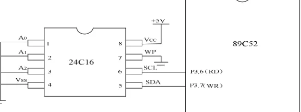
[image:5.612.161.456.211.321.2]The time of reading and writing 24C16 is about 600us, accounting for about 3% of the total program running time. The assumption is that the security of the data will not be guaranteed if the system is dropped when it happens to be reading and writing 24C16. To improve the design of the circuit, it is feasible to add the circuit protection circuit, but the system cost has been added, and the careful study of the function of 24C16 finally found a feasible solution. The controller and 24C16 hardware connection diagram are shown in figure 2.
Figure 2. The connection between the controller and the 24C16.
When initializing, the same data is stored in the same address in the 3-page storage area of 24C16. The same data will be written to these three pages each time. When reading the operation, 3 pages of data separately will be read to RAM area in order to compare. Only one page of data can be affected when the system is dropped. Compare the three data, if the three data are the same, the data is safe. Otherwise, start the calibration procedure to copy two identical data to the different page. This self-healing function is very effective.
References
[1] Data sheet of AT89C52 [EB/OL]. [2000-02]. http://www.atmel.com.
[2] Liu Leshan, The microcomputer interface technology and application in Chinese, Wuhan: Huazhong University of Science and Technology Press, 2004, pp. 66-80.