N A N O E X P R E S S
Open Access
Improvement of optical transmittance and
electrical properties for the Si quantum
dot-embedded ZnO thin film
Kuang-Yang Kuo, Chuan-Cheng Liu, Pin-Ruei Huang, Shu-Wei Hsu, Wen-Ling Chuang, You-Jheng Chen
and Po-Tsung Lee
*Abstract
A Si quantum dot (QD)-embedded ZnO thin film is successfully fabricated on a p-type Si substrate using a ZnO/Si multilayer structure. Its optical transmittance is largely improved when increasing the annealing temperature, owing to the phase transformation from amorphous to nanocrystalline Si QDs embedded in the ZnO matrix. The sample annealed at 700°C exhibits not only high optical transmittance in the long-wavelength range but also better electrical properties including low resistivity, small turn-on voltage, and high rectification ratio. By using ZnO as the QDs’matrix, the carrier transport is dominated by the multistep tunneling mechanism, the same as in a n-ZnO/p-Si heterojunction diode, which clearly differs from that using the traditional matrix materials. Hence, the carriers transport mainly in the ZnO matrix, not through the Si QDs. The unusual transport mechanism using ZnO as matrix promises the great potential for optoelectronic devices integrating Si QDs.
Keywords:Si quantum dot; ZnO thin film; Transport mechanism
Background
Recently, Si quantum dots (QDs) embedded in trad-itional Si-based dielectric matrix materials like SiO2and Si3N4have been extensively studied and successfully ap-plied to various optoelectronic devices [1-3], owing to their many unique characteristics such as highly tunable bandgap and better optical properties [4-6]. In particular, Si QD is persistently considered as a candidate for next-generation light emitters in Si photonics because of its greatly improved internal and external quantum efficien-cies [7,8]. To further improve the device performance, utilization of Si-rich Si-based dielectric materials as Si QDs’matrices has also been developed [9,10]. A suitable matrix material for Si QDs is very important for better device performance. We propose to embed Si QDs into a ZnO thin film because ZnO has many desirable fea-tures to function as Si QDs’ matrix material, e.g., wide and direct bandgap, high transparency, and highly tun-able electrical properties [11]. Hence, ZnO can serve as the Si QDs’ matrix to achieve bandgap engineering,
reduce the optical loss from the matrix’s absorption, and efficiently enhance the carrier transport efficiency for optoelectronic device application. The fabrication and fundamental optical properties of the Si QD-embedded ZnO thin films have been reported in our previous works [12,13]. In this study, improvement of optical trans-mittance and electrical properties of the Si QD-embedded ZnO thin films is investigated and discussed.
Methods
The ZnO/Si multilayer (ML) thin films with 20 bilayers are deposited on p-type Si (100) substrates or fused quartzes at room temperature using the radio-frequency (RF) magne-tron sputtering method. The sputtering powers of ZnO and Si are fixed at 75 and 110 W, and the effective thick-nesses of each ZnO and Si layer are fixed at 5 and 3 nm, respectively. After deposition, the ZnO/Si ML thin films are annealed at 500°C, 600°C, 700°C, or 800°C for 30 min in N2environment. For electrical measurements, 100-nm-thick Al and Ni metal layers are deposited on the top and bottom surfaces of devices as electrodes using a thermal coater. The Raman spectra are measured using a 488-nm diode-pumped solid-state laser (HORIBA LabRam HR, * Correspondence:potsung@mail.NCTU.edu.tw
Department of Photonics and Institute of Electro-Optical Engineering, National Chiao Tung University, 1001 Ta-Hsueh Road, Hsinchu 30010, Taiwan
HORIBA, Kyoto, Japan). The X-ray diffraction (XRD) pat-terns are examined by a Bede-D1 X-ray diffractometer with Cu Kα radiation (Bede Scientific, Engelwood, CO, USA). The transmittance spectra are obtained using a UV– vis-NIR spectrophotometer (Hitachi U-4100, Hitachi Ltd., Chiyoda, Tokyo, Japan). The cross-sectional morphologies are observed by a JSM-6500 F field-emission scanning electron microscope (SEM; JEOL Ltd., Akishima, Tokyo, Japan). The current–voltage (I-V) curves are measured using an Agilent E5270B precision measurement main-frame (Agilent Technologies Inc., Santa Clara, CA, USA).
Results and discussion
In our previous works, we demonstrated that a high Si sputtering power can assist the formation of the self-aggregated amorphous Si QDs embedded in the ZnO matrix during deposition by utilizing a ZnO/Si ML struc-ture [12]. In order to investigate the crystalline properties of the Si QDs embedded in ZnO thin films under different annealing temperatures (Tann) for a longer annealing dur-ation, Raman spectra are measured and shown in Figure 1.
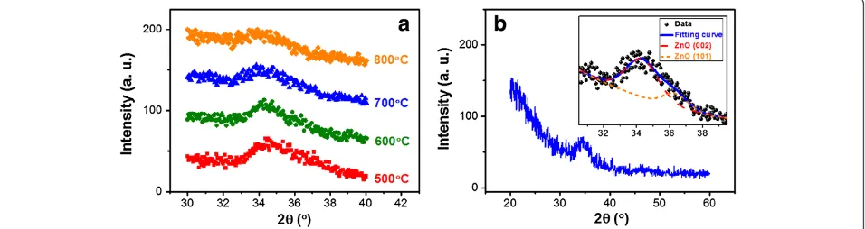
Generally, the signal of Si materials can be decomposed into three components including the peaks located at ap-proximately 480, 500 ~ 510, and 510 ~ 520 cm−1, which originated from the transverse optical (TO) modes of Si-Si vibrations in the amorphous (a-Si), intermediate (i-Si), and nanocrystalline Si (nc-Si) phases [14]. The corresponding crystalline volume fractions of Si (fc) obtained from fitting the curves are shown in the inset of Figure 1 [14]. The nc-Si phase is formed in the ZnO matrix and significantly in-creased by increasingTannwhenTannis higher than 600°C. This indicates that a higherTann can largely enhance the crystalline quality of Si QDs embedded in the ZnO matrix. Since the crystalline properties of the ZnO matrix can influence its optical and electrical properties [15], the XRD patterns of the Si QD-embedded ZnO thin films annealed at different temperatures are examined and shown in Figure 2a, fine-scanned from 30° to 40°. A main diffraction signal is observed at approximately 34.5° for all the samples. As shown in Figure 2b and its inset, this sig-nal can be decomposed into two components in Gaussian form with peaks located at about 34.3° and about 36.3°, which are contributed from (002) and (101) orientations of ZnO [16]. In Figure 2a, the crystallization intensity of the ZnO matrix is slightly reduced when increasingTann. This may be due to the increased interior film stress resulting from the phase transformation of a- to nc-Si QDs. From the results of Raman and XRD measurements, we show that the nc-Si QDs embedded in the crystalline ZnO matrix can be achieved by aTannhigher than 600°C.
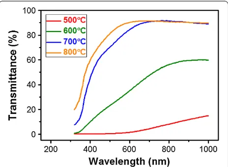
[image:2.595.58.291.89.256.2]The optical transmittance spectra of the Si QD-embedded ZnO thin films under differentTannare shown in Figure 3. The transmittance in the long-wavelength (long-λ) range (>600 nm) clearly increases when increas-ing Tann. Since higher Tann can obviously enhance the crystallization of Si QDs, the improved optical transmit-tance in the long-λ range can be attributed to the de-creased absorbance from a-Si QDs due to the inde-creasedfc of Si QDs [5]. It is worthy to note that high transmittance of approximately 90% in the long-λ range under a Tann
Figure 1Crystalline properties of Si QDs.Raman spectra of the Si QD-embedded ZnO thin films under differentTann. The inset shows
the corresponding crystalline volume fractions of Si (fc).
Figure 2Crystalline properties of ZnO matrix. (a)XRD patterns fine-scanned from 30° to 40° of the Si QD-embedded ZnO thin films under differentTann.(b)Full XRD pattern of the Si QD-embedded ZnO thin film annealed at 700°C. The inset shows the curve fitting result for the main
[image:2.595.61.539.568.695.2]higher than 700°C can be achieved and is close to those using the traditional matrix materials [5]. From the above results, it is clear that better crystallization of Si QDs in the ZnO matrix is required to decrease the absorption from a-Si QDs and thus efficiently reduce the optical loss in the long-λ range for better optoelectronic device performance. We find that a high-enoughTann for the Si QD-embedded ZnO thin film is critical to significantly im-prove the optical properties.
The images of the Si QD-embedded ZnO thin films after annealing are examined by SEM. The local film promi-nences are observed when Tann is higher than 600°C. Figure 4a shows the cross-sectional SEM image of a sam-ple annealed at 700°C. The local film prominence density and diameter in average are estimated and shown in Figure 4b. The prominence density increases almost linearly from 5.5 to 7.6 ones per 10 × 10 μm2 when in-creasing Tann from 600°C to 800°C with a close average diameter of about 2μm. According to Raman spectra, the phase transformation of a- to nc-Si QDs happens when
Tann is larger than 600°C, and fc also increases with
increasingTann from 600°C to 800°C. This strong correl-ation betweenfcand prominence density means that the volume variation from the phase transformation of a- to nc-Si QDs embedded in the ZnO matrix during annealing can produce an interior film stress and lead to the occur-rence of local film prominences.
To understand the electrical properties of the Si QD-embedded ZnO thin films, the vertical resistivity (ρ) is calculated from the slope of the I-Vcurve under a high forward bias region of 4 ~ 5 V. When increasing Tann, theρ can be reduced by the improved crystalline quality of Si QDs but also raised by the increased film promin-ence density and degraded crystalline quality of the ZnO matrix. Figure 5a shows the obtained ρ under different
[image:3.595.58.290.89.259.2]Tann, which slightly increases when increasingTannfrom 500°C to 700°C but still keeps a low resistivity of approxi-mately 104Ω cm, significantly lower than that (approxi-mately 108Ωcm) of the intrinsic Si QDs embedded in a SiO2matrix [17,18]. It is evident that using ZnO as matrix can overcome the issue of highly resistive nature of the traditional Si-based dielectric matrix materials, and 104 times improvement ofρis obtained. Theρlargely increases for the sample annealed at 800°C, which may have resulted from the excess film prominences produced during annealing since the film prominences will lead to local broken circuit regions at the interface of film/substrate and significantly increase the resistivity. Hence, we can con-clude that annealing at 700°C is a more suitable annealing condition to have better crystallization of Si QDs in the crystalline ZnO matrix, low ρ, and high transmittance in the long-λrange. The logarithmicI-Vcurve of the sample annealed at 700°C is shown in Figure 5b, and its inset shows the corresponding linearI-Vcurve in magnification. It clearly exhibits not only a good rectification ratio of 3.4 × 10³ at ±5 V but also a low turn-on voltage (Vt) of 0.48 V, which agrees with the reported results of the n-ZnO/p-Si heterojunction (HJ) diode [19,20]. Even though the Si QDs are embedded in the ZnO matrix, we show that the fabricated ZnO thin film on p-Si can still
[image:3.595.56.539.574.703.2]Figure 3Optical properties.Optical transmittance spectra of the Si QD-embedded ZnO thin films under differentTann.
possess good p-n HJ diode behavior with large rectifica-tion ratio and lowVt.
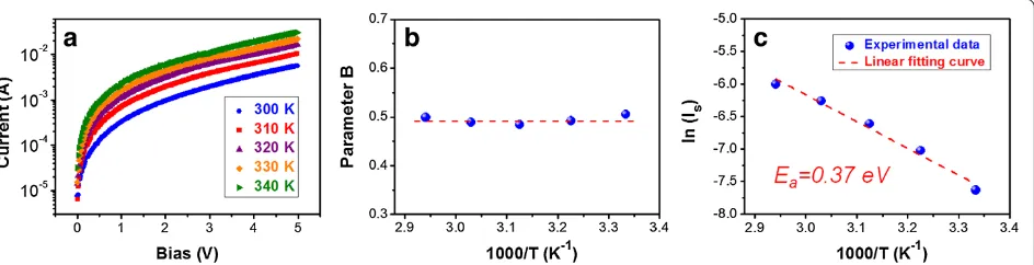
To investigate the carrier transport mechanism, the temperature-dependent forwardI-Vcurves of the sample annealed at 700°C are examined and shown in Figure 6a. The I-Vcurves exhibit the typical temperature depend-ence of a p-n junction diode. The current clearly in-creases as we raise the measurement temperature (Tmeas). In the low bias region (smaller than approxi-mately 0.5 V), the currents can be well fitted to be pro-portional to aboutV1.2 for differentTmeas, which slightly deviates from the ohmic behavior. This means that the surface states and/or an inherent insulating SiO2 thin layer at the interface of the n-ZnO matrix/p-Si substrate has influence on the transport of carriers [21]. In the high bias region (larger than approximately 0.5 V), the for-ward currents can be well expressed byI=Is[exp(BV)−1] for different Tmeas, where Is is the reverse saturation current and parameterBis a coefficient dependent or in-dependent on temperature decided by the dominant car-rier transport mechanism [21,22]. The fitted results for parameterBare shown in Figure 6b, which reveal that the parameter B is almost invariant for different Tmeas. This independence ofTmeasindicates that the carrier transport is dominated by the multistep tunneling mechanism,
[image:4.595.58.540.89.221.2]which had been reported by Zebbar et al. and Dhananjay et al. for the n-ZnO/p-Si HJ diode [21,23]. The multistep tunneling process usually occurs at the HJ region of the n-ZnO matrix and p-Si substrate, which is attributed to the recombination of electrons, tunneling from ZnO into the empty gap states in the p-Si substrate, and holes, tunnel-ing through the HJ barrier from the p-Si substrate to the n-ZnO matrix between the empty states [21,23]. Hence, our results show that the carriers in the Si QD-embedded ZnO thin film mainly transport via the ZnO matrix but not through Si QDs with direct, resonant, or phonon-assisted tunneling mechanisms, as reported for Si QDs embedded in the traditional matrix materials [24,25]. According to the multistep tunneling mechanism, the temperature dependence ofIsis given by the relation,Is∝ exp(−Ea/kT), where Ea is the activation energy, k is Boltzmann’s constant, and T is the absolute temperature [21,23]. Figure 6c shows the Arrhenius plot of ln(Is) versus 1,000/T. A linear relationship is clearly observed, which further confirms that the dominating carrier transport process is the multistep tunneling mechanism [19,21-23]. The Ea of around 0.37 eV obtained from the Arrhenius plot is a little larger than those of the reported n-ZnO/p-Si HJ diodes, which are usually smaller than 0.3 eV [19,21-23]. This means that the thermally activated
Figure 5Electrical properties. (a)Vertical resistivity of the Si QD-embedded ZnO thin films under differentTann.(b)LogarithmicI-Vcurve of the
sample annealed at 700°C. The inset shows the linearI-Vcurve in magnification.
[image:4.595.66.538.584.705.2]carriers are partially contributed from the embedded Si QDs since the intrinsic Si QDs can possessEalarger than 0.4 eV [17,26]. Thus, we can conclude that the Si QDs em-bedded in ZnO matrix also contribute the carriers, and those carriers will partially escape from Si QDs into the ZnO matrix and transport inside. The largely improved resistivity suggests that the carriers transporting in the ZnO matrix can have a much better transport efficiency than those tunneling through barriers in the traditional matrix materials. With the unique carrier transport mech-anism and better electrical properties, we believe that the Si QD thin films will have great potential for optoelec-tronic device application by using ZnO as matrix material.
Conclusions
In summary, we successfully fabricate a nc-Si QD-embedded ZnO thin film on a p-Si substrate using a ZnO/Si ML deposition structure. Our results indicate that the optical transmittance can be largely enhanced by increasingTann owing to the phase transformation of a- to nc-Si QDs embedded in the ZnO matrix, and up to about 90% transmittance in the long-λrange under aTann higher than 700°C is obtained. The Si QD-embedded ZnO thin film annealed at 700°C exhibits good diode behavior with a large rectification ratio of approximately 103at ±5 V and significantly lower resistivity than that using the SiO2 matrix material (104 times improvement). From temperature-dependentI-Vcurves, we find that the car-riers transport mainly via the ZnO matrix, not through Si QDs, which is dominated by the multistep tunneling mechanism as in the n-ZnO/p-Si HJ diode. The unique transport mechanism differing from those using the traditional Si-based dielectric matrix materials can lead to much better carrier transport efficiency and electrical properties. Hence, we show that the Si QD thin film using the ZnO matrix material is very advantageous and has potential for optoelectronics device application.
Competing interests
The authors declare that they have no competing interests.
Authors’contributions
KYK and PTL carried out the experimental design and analysis and drafted the manuscript. CCL carried out the experimental fabrication and measurements. PRH, SWH, WLC, and YJC participated in the experimental fabrication. All authors read and approved the final manuscript.
Acknowledgements
This work is supported by Taiwan’s National Science Council (NSC) under contract number NSC-101-3113-P-009-004. The authors would like to thank the help from the Center for Nano Science and Technology (CNST) of National Chiao Tung University and National Nano Device Laboratories (NDL) in Taiwan.
Received: 4 September 2013 Accepted: 2 October 2013 Published: 23 October 2013
References
1. Anopchenko A, Marconi A, Wang M, Pucker G, Bellutti P, Pavesi L: Graded-size Si quantum dot ensembles for efficient light-emitting diodes.
Appl Phys Lett2011,99:181108.
2. Lin GR, Lin CJ, Lin CK, Chou LJ, Chueh YL:Oxygen defect and Si nanocrystal dependent white-light and near-infrared
electroluminescence of Si-implanted and plasma-enhanced chemical-vapor deposition-grown Si-rich SiO2.J Appl Phys2005,97:094306.
3. Perez-Wurfl I, Hao X, Gentle A, Kim DH, Conibeer G, Green MA:Si nanocrystal p-i-n diodes fabricated on quartz substrates for third generation solar cell applications.Appl Phys Lett2009,95:153506. 4. Garoufalis CS, Zdetsis AD:High level ab initio calculations of the optical
gap of small silicon quantum dots.Phys Rev Lett2001,87:276402. 5. Mirabella S, Agosta R, Franzò G, Crupi I, Miritello M, Savio RL, Stefano MAD,
Marco SD, Simone F, Terrasi A:Light absorption in silicon quantum dots embedded in silica.J Appl Phys2009,106:103505.
6. Kang Z, Liu Y, Tsang CHA, Ma DDD, Fan X, Wong NB, Lee ST:Water-soluble silicon quantum dots with wavelength-tunable photoluminescence.
Adv Mater2009,21:661–664.
7. Lin GR, Lin CJ, Kuo HC:Improving carrier transport and light emission in a silicon-nanocrystal based MOS light-emitting diode on silicon nanopillar array.Appl Phys Lett2007,91:093122.
8. Cheng CH, Lien YC, Wu CL, Lin GR:Mutlicolor electroluminescent Si quantum dots embedded in SiOxthin film MOSLED with 2.4% external
quantum efficiency.Opt Express2013,21:391–403.
9. Lin GR, Pai YH, Lin CT, Chen CC:Comparison on the electroluminescence of Si-rich SiNxand SiOxbased light-emitting diodes.Appl Phys Lett2010,
96:263514.
10. Conibeer G, Green MA, Konig D, Perez-Wurfl I, Huang S, Hao X, Di D, Shi L, Shrestha S, Puthen-Veetil B, So Y, Zhang B, Wan Z:Silicon quantum dot based solar cells: addressing the issues of doping, voltage and current transport.Prog Photovolt Res Appl2011,19:813–824.
11. Özgür Ü, Alivov YI, Liu C, Teke A, Reshnikov MA, Dogan S, Avrutin V, Cho SJ, Morkoç H:A comprehensive review of ZnO materials and devices.J Appl Phys2005,98:041301.
12. Kuo KY, Hsu SW, Chuang WL, Lee PT:Formation of nano-crystalline Si quantum dots in ZnO thin-films using a ZnO/Si multilayer structure.
Mater Lett2012,68:463–465.
13. Kuo KY, Hsu SW, Huang PR, Chuang WL, Liu CC, Lee PT:Optical properties and sub-bandgap formation of nano-crystalline Si quantum dots embedded ZnO thin film.Opt Express2012,20:10470–10475. 14. Cheng Q, Tam E, Xu S, Ostrikov KK:Si quantum dots embedded in an
amorphous SiC matrix: nanophase control by non-equilibrium plasma hydrogenation.Nanoscale2010,2:594–600.
15. You JB, Zhang XW, Fan YM, Yin ZG, Cai PF, Chen NF:Effect of deposition conditions on optical and electrical properties of ZnO films prepared by pulsed laser deposition.Appl Surf Sci2002,197–198:363–367.
16. Sundaram KB, Khan A:Characterization and optimization of zinc oxide films by r.f. magnetron sputtering.Thin Solid Films1997,295:87–91. 17. Hao XJ, Cho EC, Scardera G, Shen YS, Bellet-Amalric E, Bellet D, Conibeer G,
Green MA:Phosphorus-doped silicon quantum dots for all-silicon quantum dot tandem solar cells.Sol Energy Mater Sol Cells2009,93:1524–1530. 18. Di D, Xu H, Perez-Wurfl I, Green MA, Conibeer G:Improved nanocrystal
formation, quantum confinement and carrier transport properties of doped Si quantum dot superlattices for third generation photovoltaics.
Res Appl: Prog Photovolt2013,21:569–577.
19. Lee JD, Park CY, Kim HS, Lee JJ, Choo YG:A study of conduction of ZnO film/p-Si heterojunction fabricated by photoinduced electrodeposition under illumination.J Phys D Appl Phys2010,43:365403.
20. Mridha S, Basak D:Ultraviolet and visible photoresponse properties of n-ZnO/p-Si heterojunction.J Appl Phys2007,101:083102.
21. Zebbar N, Kheireddine Y, Mokeddem K, Hafdallah A, Kechouane M, Aida MS:Structural, optical and electrical properties of n-ZnO/p-Si heterojunction prepared by ultrasonic spray.Mater Sci Semicond Process
2011,14:229–234.
22. Zhang Y, Xu J, Lin B, Fu Z, Zhong S, Liu C, Zhang Z:Fabrication and electrical characterization of nanocrystalline ZnO/Si heterojunctions.
Appl Surf Sci2006,252:3449–3453.
23. Dhananjay, Nagaraju J, Krupanidhi SB:Investigations on zinc oxide thin films grown on Si (100) by thermal oxidation.Mater Sci Eng B2007,
24. Osinniy V, Lysgaard S, Kolkovsky V, Pankratov V, Larsen AN:Vertical charge-carrier transport in Si nanocrystal/SiO2multilayer structures.
Nanotechnology2009,20:195201.
25. Veettil BP:Modelling and characterization of carrier transport through nanostructures.PhD thesis. University of New South Wales, School of Photovoltaic and Renewable Energy Engineering; 2012.
26. Fangsuwannarak T:Electronic and optical characterisations of silicon quantum dots and its applications in solar cells.PhD thesis. University of New South Wales, Centre of Excellence for Advanced Silicon Photovoltaics and Photonics; 2007.
doi:10.1186/1556-276X-8-439
Cite this article as:Kuoet al.:Improvement of optical transmittance and
electrical properties for the Si quantum dot-embedded ZnO thin film.
Nanoscale Research Letters20138:439.
Submit your manuscript to a
journal and benefi t from:
7 Convenient online submission
7 Rigorous peer review
7 Immediate publication on acceptance
7 Open access: articles freely available online
7 High visibility within the fi eld
7 Retaining the copyright to your article