Helmut Fo¨ll
Received: 15 April 2010 / Accepted: 28 April 2010 / Published online: 14 May 2010
ÓThe Author(s) 2010. This article is published with open access at Springerlink.com
Abstract The growth mechanism of currentline-oriented pores in n-type InP has been studied by Fast-Fourier-Transform Impedance Spectroscopy (FFT IS) applied in situ during pore etching and by theoretical calculations. Several pore growth parameters could thus be extracted in situ that are otherwise not obtainable. These include the space-charge-region (SCR) width, the SCR potential, the capacitance at the pore tips, and the avalanche breakdown field strength. It could be demonstrated that the system adjusts itself in such a way that the potential across the space-charge-region at the pore tips is kept constant within a certain bandwidth of the applied potential. This provides for a constant field strength at the pore tips, ensuring that avalanche breakdown occurs, generating the necessary holes for the electrochemical dissolution of InP.
Keywords Porous semiconductorsInP
Impedance spectroscopy
Introduction
Porous semiconductors have been envisioned for the use in a broad range of applications, and substantial R&D efforts have been made in this direction [1–7]. In the majority of the proposed applications, the detailed morphology of the por-ous structure is decisive for the functioning of the applica-tion. Morphology parameters like pore diameter and shape, pore wall thickness and roughness, or pore density have to be
established with often a rather high precision, i.e. for optical applications [4,8]. To meet precise specifications, a thor-ough understanding of the pore formation mechanism is needed but not yet established for any pore system, including the thoroughly investigated porous Si. For deeper insights into general pore etching mechanisms, InP can be consid-ered as a model semiconductor, which allows easier sys-tematic investigations than, e.g., Si because only two kinds of pores seem to exist, which are quite different in their general behavior. Changing external parameters like the etching current density or the potential can easily control the respective pore formation modes. Both pore growth modes seem to embody the simplest case of electrochemical pore etching, where only one main electrochemical reaction occurs, in contrast to systems like Si, where always several reactions occur, making the system harder to analyze.
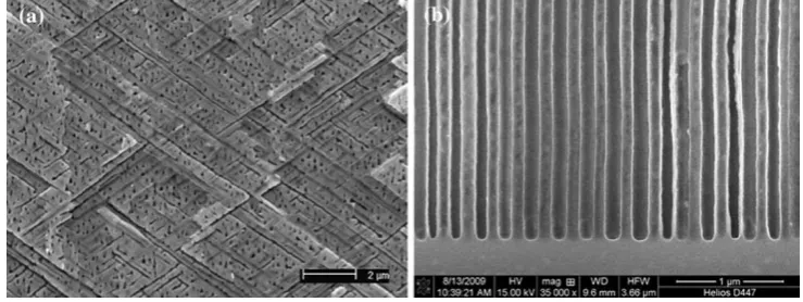
The two pore types present in InP are the so-called crystallographical pores (crystos) and currentline pores (curros). The crysto pores always grow into the\111[B directions of the InP crystal [9, 10], Fig.1a gives an example. The pores have a triangular cross section and pore tips and grow along the two available ‘‘downward’’ \111[B directions of the crystal (‘‘channels’’ or lines in the plane of view in Fig. 1a) and into the two available ‘‘upward’’\111[B directions, intersecting the plane of view in Fig.1a, giving the appearance of triangular holes. Figure1b shows a typical example of curro pores in (100)n-type InP [11,12]. The pores have a circular cross-section and semispherical pore tips. They grow in direction of the current flow, i.e. usually perpendicular to the sample surface, independent of the crystal orientation.
The growth mechanism of crysto pores has already been studied by FFT Impedance Spectroscopy and could be successfully modeled by a stochastic model of the ‘‘current burst’’ type [13], which has been implemented into a
M. Leisner (&)J. CarstensenH. Fo¨ll
Institute for Materials Science, Christian-Albrechts-University of Kiel, Kaiserstrasse 2, 24143 Kiel, Germany
e-mail: [email protected]
Monte-Carlo simulation [14,15]. This work will focus on the growth mechanism behind the currentline pores, expanding the work presented in [16]. Results of the in situ FFT impedance spectroscopy [17] will be analyzed.
Experimental Procedure
All pores have been etched into single-crystalline n-type InP wafers. The orientation was (100), and three different doping concentrationsNDhave been used: 11017, 81017,
and 31018cm-3. The sample size wasA=0.25 cm2. The samples have been etched in an electrochemical double cell, the basic set-up is described in detail in [18]. 6 wt% HCl aq. has been used as electrolyte. All experiments have been conducted at T=20°C under constant etching potential. The dc potential used was in the range of 6–8 V forND=11017cm-3, 4–7 V forND=81017 cm-3, and
2–4 V for ND=31018 cm-3. In these potential ranges
‘‘good quality’’ pores can be obtained, i.e. pores with straight and smooth pore walls, growing perpendicular to the surface. In the beginning of the experiments, a high-potential pulse has been applied for 1 s to guarantee a homogeneous nucleation of the pores. Typical etching times were between 5 and 70 min, resulting in pore depths up to 500lm, i.e. aspect ratios of[1,000.
During all experiments, FFT impedance spectra (FFT IS) [17,19] were recorded every 1.5 s. The measurement signal contained 28 frequencies between 30 Hz and 20 kHz. The spectra obtained were fitted to a model, which allowed on-line extraction of the model parameters.
Results
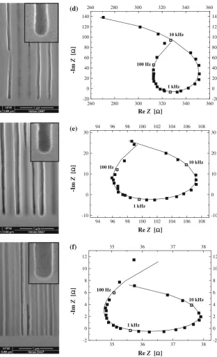
Regular arrays of currentline pores can be etched into InP for all three doping concentrations investigated. Figure2a–c
shows cross-sectional SEM images of typical pore struc-tures. It can be seen that the pores grow perpendicular to the surface and have a fairly round tip, which gets slightly flatter with increasing ND (see the insets). The pore
diameterwpore=130 nm is pretty much the same in all
cases and thus can be seen as being independent of the doping concentrations and of the etching potentials used as long as they are inside the potential ranges for good quality pores. The pore wall thicknessdwall, on the other
hand, strongly depends on the doping concentrationND; it
decreases with increasingND. As is already known from
the literature [20], an analysis of the top view of pores showed that these pores grow in a self-organized hexag-onal lattice.
Figure2d–f shows typical FFT IS spectra recorded during the etching for the three respective doping con-centrations shown in a–c after 38 min of etching. The dots represent the measured data, which were fitted (line) by
ZðxÞ ¼RSþ R1 1þixR1C1
þ R2
1þ ð1þiÞ ffiffiffiffiffiffiffiffixs2
p
þ R3
1þixR3C3; ð1Þ
where Z(x) is the model impedance,RS is a serial
resis-tance,R1,R2, andR3are transfer resistances,C1andC3are
capacitances, ands2is a time constant. The measurement
frequencies are indicated in the graphs. It can be seen that Eq. 1 is able to fit the data for all three doping concen-trations very well, even though the absolute numbers on the axes are quite different between the experiments. It should be mentioned that the fit is just as good to the 500–2,800 FFT IS obtained through one etching experiment after the short nucleation phase (\1 min), lending credibility to the model used. The amount of data generated will easily exceed the page limitation of any publication, in what follows we will therefore focus on some selected aspects of the model that yield the deepest insights into the pore etching mechanisms.
[image:2.595.112.482.60.199.2]Discussion
Figure3 shows the product of the etching current I with R1?R2as measured by FFT IS, which has the units of a
voltage (or potential). Shown are several curves for each doping concentration, which correspond to experiments with different etching potentials in the aforementioned etching potential window that yielded good quality pores. The I (R1?R2) curves are independent of the etching
potential, only depend on the doping concentrationND, and
are essentially constant after an initial nucleation phase. In the nucleation phase, the pores do not yet grow in the close-packed hexagonal geometry, and thus the active area differs and affectsR1andR2; therefore,I(R1?R2)
devi-ates from the constant value in this range. It is tempting to assume that the product I (R1?R2):=USCR is the
potential drop over the space-charge-region (SCR) and in what follows we will argue that this is indeed the case.R1
-20 0
-20 0 1 kHz
-Im
Z
[
Ω
]
-Im
Z
[
Ω
]
Re Z [Ω]
Re Z [Ω] Re Z [Ω] (b)
-10 0 10 20 30
-10 0 10 20 30
100 Hz
10 kHz
1 kHz
(e)
(c)
-2 0 2 4 6 8 10 12
260 280 300 320 340 360
94 96 98 100 102 104 106 108
94 96 98 100 102 104 106 108
35 36 37 38
35 36 37 38
-2 0 2 4 6 8 10 12
100 Hz
1 kHz
10 kHz
(f) after 38 min of etching. The
[image:3.595.228.541.55.569.2]and C1 must then be interpreted as the resistance and
capacitance of the SCR, while R2 and s2 represent the
avalanche breakdown mechanism, which is generating the holes required to etch the semiconductor anodically.
To prove our claim, we have calculated USCR as a
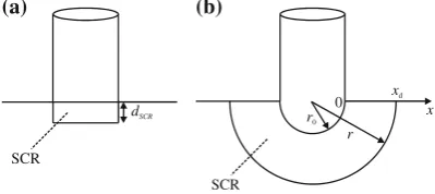
function of doping and pore tip geometry. To do this, the pore geometry (hexagonal lattice arrangement, pore diameter, pore wall thickness) has to be known to some extent, and these values have been determined by SEM. To obtain the properties of the SCR, the Poisson equation has to be solved, yielding the SCR thickness, capacitance and field strength at the pore tips. This is a standard textbook problem for the planar geometry as illustrated in Fig.4a, cf. [21]. Pore walls need not to be considered, since (by definition) no appreciable current flows through pore walls. For a semi-spherical geometry, as presented in Fig.4b, a solution of the Poisson equation is given in [22]. These two geometries describe the extremes for the real pore tip shape, which lies between the perfect semi-spherical geometry and the planar geometry, dependent on ND, as
shown in the insets of Fig.2. For all calculations,USCR, as
described in Fig.3, serves as input parameter.
The thickness of the SCR has been calculated for both geometries and for all three doping concentrations; it is tabulated in Table1. It is given as 2 dSCR, since it is
commonly expected that the pore wall thickness is defined by twice the distance of the space-charge-region, leading to an overlap of the SCRs and thus insulating pore walls, which cannot be further electrochemically dissolved, since no holes are present. Table1therefore also shows the pore wall thickness dwall, as measured by SEM. It can be seen
that the values are in good agreement, and that the ND
dependence is correct.
The capacitance of the SCR at the pore tipsCSCRcan be
calculated analogously for both geometries. Figure5
shows the calculated values for the planar (boxes) and semi-spherical (circles) geometry. The stars represent the data measured by FFT IS (C1). It can be seen that these
values always lie in between the boundaries that describe the two extreme geometries. Furthermore, the values move to the planar boundary with increasing ND. This reflects
very well the change in pore tip shape from round to flat with increasingND, which is visible in the insets of Fig.2.
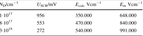
The last SCR quantity that has been calculated is the field strength at the pore tips Ecalc. The calculated values 0
200 400 600 800 1000
0 10 20 30 40 50
0 10 20 30 40 50
0 200 400 600 800 1000
ND = 3*1018 cm-3
N D = 8*10
17
cm-3
ND = 1*1017 cm-3
I
*(
R 1
+
R 2
) [mV]
t [min]
Fig. 3 Potential dropUSCR:=I (R1?R2) over the
space-charge-region (SCR). Several lines correspond to different etching potentials in the aforementioned respective etching potential windows. Thecurves
are constant after an initial nucleation phase and dependent onND
SCR
dSCR
(a)
0
SCR
x xd
r0
r
(b)
[image:4.595.53.286.54.225.2]Fig. 4 Geometries used for theoretical calculations of the SCR properties.aPlanar geometry.bSemi-spherical geometry
Table 1 Pore wall thicknessdwallas measured from Fig.2is in good
agreement with twice the value of the SCR width dSCR, which has
been calculated for * planar geometry and ** semispherical geometry
ND/cm-3 dwall/nm
measured
2dSCR/nm*
calculated
2dSCR/nm**
calculated
11017 148 230 168
81017 94 62 55
31018 27 22 21
0,0 0,1 0,2 0,3 0,4
0 5 10 15 20 25 30
0 5 10 15 20 25 30
0,0 0,1 0,2 0,3 0,4 Semispherical Geometry
Planar Geometry Measured Data
C SCR
[
μ
F]
N D * 10
17
[cm-3]
Fig. 5 Capacitance of the SCR at the pore tipsCSCR. Thesquares
[image:4.595.306.545.93.164.2] [image:4.595.70.270.301.390.2] [image:4.595.309.545.489.663.2]are listed in Table2. These values are compared to theo-retical values of the maximum field strength Emfor
ava-lanche breakdown, which can be calculated after [21,23] by
Em¼ Eg 1:1 eV 3=4
e1r=2 ND 1017cm3
1=8
1:96 V/cm, ð2Þ
whereEgis the bandgap anderthe dielectric constant of the
semiconductor. Please note that the values ofEmare for an
all solid InP pn-junction, the best comparison available, since no data for the InP-HCl junction exists. Nevertheless, Table2shows that the values are in good agreement with Ecalc, as calculated by FFT IS.
This last finding supports the fact that the part of the impedance described by R2 and s2 is the avalanche
breakdown mechanism, indeed. This interpretation is also capable of explaining the negative (differential) imped-ance, i.e. the ‘‘inductive’’ loop, which is always present.
All things considered, the results strongly support the validity of the model expressed in Eq.1and the interpre-tation of parameters extracted.
We believe that the third process represents the diffuse layer inside the pores, where R3 and C3 describe the
respective resistance and capacitance. This claim has not yet been supported by theoretical calculations, but might yield further insights in the near future.
Conclusion
It has been demonstrated that currentline pore growth in InP is governed by a constant potentialUSCRin the SCR,
which keeps the field strength required for avalanche breakdown constant (since the pore tip shape does not change). This mechanism is present at all three investigated doping concentrations ND, for which hexagonally close
packed pore structures with different pore wall thicknesses, but constant pore diameter have been observed. It was
References
1. V. Lehmann, Electrochemistry of silicon (Wiley-VCH, Wein-heim, 2002)
2. H. Fo¨ll, M. Leisner, A. Cojocaru, J. Carstensen, Materials, accepted for publication
3. V. Kochergin, H. Fo¨ll,Porous semiconductors: optical properties and applications(Springer, London, 2009)
4. M.J. Sailor,Porous silicon in practice: preparation (Character-ization and Applications, Wiley-VCH, 2010)
5. J.-N. Chazalviel, F. Ozanam, Macropores in p-type silicon, in
Ordered porous nanostructures and applications, ed. by R.B. Wehrspohn (Springer, Berlin, 2005)
6. S. Ossicini, L. Pavesi, F. Priolo, Light emitting silicon for microphotonics(Springer, Berlin, 2003)
7. A. Sa0ar, J. Nanophoton. 3, 032501 (2009)
8. V. Kochergin, H. Fo¨ll, Mater. Sci. Eng. R52(4–6), 93 (2006) 9. H. Fo¨ll, S. Langa, J. Carstensen, S. Lo¨lkes, M. Christophersen,
I.M. Tiginyanu, Adv. Mater.15, 3–183 (2003)
10. T. Takizawa, S. Arai, M. Nakahara, Japan J. Appl. Phys.33(2, 5A), L643 (1994)
11. H. Fo¨ll, S. Langa, J. Carstensen, M. Christophersen, I.M. Tigi-nyanu, III-Vs Review16(7), 42 (2003)
12. E. Kikuno, M. Amiotti, T. Takizawa, S. Arai, Japan J. Appl. Phys.34(1, 1), 177 (1995)
13. J. Carstensen, R. Prange, G.S. Popkirov, H. Fo¨ll, Appl. Phys. A
67(4), 459 (1998)
14. M. Leisner, J. Carstensen, A. Cojocaru, H. Fo¨ll, ECS Trans.
16(3), 133 (2008)
15. M. Leisner, J. Carstensen, H. Fo¨ll, ECS Trans.19(3), 321 (2009) 16. M. Leisner, J. Carstensen, A. Cojocaru, H. Fo¨ll, Phys. Stat. Sol.
(c)206, 7–1566 (2009)
17. G.S. Popkirov, R.N. Schindler, Rev. Sci. Instrum. 63, 5366 (1992)
18. S. Langa, I.M. Tiginyanu, J. Carstensen, M. Christophersen, H. Fo¨ll, Electrochem. Solid-State Lett.3(11), 514 (2000) 19. J. Carstensen, E. Foca, S. Keipert, H. Fo¨ll, M. Leisner,
A. Cojocaru, Phys. Stat. Sol. (a)205, 11–2485 (2008)
20. S. Langa, I.M. Tiginyanu, J. Carstensen, M. Christophersen, H. Fo¨ll, Appl. Phys. Lett.82, 2–278 (2003)
21. S.M. Sze,Physics of semiconductor devices(Wiley & Sons, New York, 1981)
[image:5.595.52.290.83.144.2]