N A N O E X P R E S S
Open Access
Wavelength-Controlled Photodetector
Based on Single CdSSe Nanobelt
Xinmin Li
1,3, Qiuhong Tan
1,2,3, Xiaobo Feng
1,2,3, Qianjin Wang
1,2,3and Yingkai Liu
1,2,3*Abstract
CdSSe nanobelts (NBs) are synthesized by thermal evaporation and then characterized by scanning electron microscopy (SEM), X-ray diffraction (XRD), transmission electron microscopy (TEM), high-resolution electron microscopy (HRTEM), X-ray photoelectron spectroscopy (XPS), photoluminescence (PL), and cathodoluminescence (CL). It is found that the CdSSe NBs have a good morphology and microstructure without defects. CL is sensitive to the defects of CdSSe NBs; thus, we can select single nanobelt with homogeneous CL emission to prepare a detector. Based on it, the photodetector of single CdSSe NB was developed and its photoelectric properties were investigated in detail. It is found that under illumination of white light and at the bias voltage of 1 V, the
photocurrent of a single CdSSe nanobelt device is 1.60 × 10⁻⁷A, the dark current is 1.96 × 10⁻¹⁰A, and the ratio of light current to dark one is 816. In addition, the CdSSe nanobelt detector has high photoelectric performance with spectral responsivity of 10.4 AW−1and external quantum efficiency (EQE) of 19.1%. Its rise/decay time is about 1.62/4.70 ms. This work offers a novel strategy for design wavelength-controlled photodetectors by adjusting their compositions.
Keywords:CdSSe nanobelts, Optical properties, Cathodoluminescence, Photodetector
Background
Recently, semiconductor nanomaterials have been widely studied as optoelectronic devices, such as light emitting diodes [1,2], photovoltaic devices [3], solar cell [4,5], elec-trocatalytic H2 generation [6, 7], and photodetectors [8–10]. CdS and CdSe are II–VI semiconductor materials with the bandgap at room temperature of 2.42 and 1.74 eV, respectively. They are considered to be the best materials for the fabrication of photodetectors due to their bandgap corresponding to the absorption wavelength in the visible light region [11,12].
One-dimensional nanostructures such as nanowires [13], nanobelts [14], and nanotubes [15] have been used in sensors and photodetectors due to their high surface-to-volume ratios, physical properties, and chemical properties [16]. Among them, some nanostructures such as ZnO [17], CdS [18], CdSe [19], MoS2 [20], ZnxCd1−xSe
[21], CdS1−xSex[22], and ZnxCd1−xS [23] have been used
in fabrication photodetectors. Pan et al. reported that the photodetector based on CdS0.49Se0.51/CdS0.91Se0.09 hetero-structure has a good performance [24]. However, how to develop a high response and selectivity detector with excel-lent performance is still a challenge.
In this work, the CdSSe nanobelts (NBs) were synthe-sized by thermal evaporation. We undertake the fabrication and characterization of single CdSSe device. After that, the photoelectric properties of single CdSSe NB device were systematically investigated. Based on it, we carried out the cathodoluminescence (CL) of CdSSe NB at room temperature and low temperature and found that CL is sensitive to the defects of CdSSe NBs. Therefore, we choose nanobelts with perfect microstructures to design devices by CL so that they can achieve our desired properties.
Methods
Preparation of CdSSe Nanobelts
Single-crystal CdSSe NBs were prepared by thermal evapor-ation. For synthesis of CdSSe NBs, the mixture of pure CdS powders (99.99 wt%) and CdSe powders (9.99 wt%) pre-mixed in the weight ratio of 1:1 was put into a ceramic boat. The ceramic boat was placed in the middle of the
* Correspondence:[email protected] 1
Institute of Physics and Electronic Information, Yunnan Normal University, Kunming 650500, People’s Republic of China
2Yunnan Key Laboratory of Opto-electronic Information Technology,
Kunming 650500, People’s Republic of China
Full list of author information is available at the end of the article
quartz tube. A silicon substrate coated with about 10-nm Au film was placed into the tube; the distance of silicon substrate and ceramic boat was about 5–7 cm. The furnace was heated to 820 °C and was then maintained for 2 h. Finally, the furnace naturally cooled to room temperature. The nanobelts with different compositions were deposited on the different position of the Si substrate. In the whole experiment, Ar gas was flown at 20 sccm, and the pressure inside the tube was kept at 112 Torr.
Material Characterization
The morphology, structure, and composition of the nano-belts were characterized by scanning electron microscopy (SEM), X-ray diffraction (XRD), transmission electron
microscopy (TEM), high-resolution electron microscopy (HRTEM), and X-ray photoelectron spectroscopy (XPS). The PL spectra were measured under 532-nm laser excita-tion. CL spectra of CdSSe NBs were measured at room temperature and low temperature by a cathodolumines-cence (CL) (Gatan monocle CL4) system installed on the scanning electron microscopy (Quanta FEG 250).
Fabrication of Nanobelt Device
Ti/Au electrodes were deposited on the two ends of a single nanobelt dispersed on Si substrate with a 500-nm-thick SiO2 layer, and then, the device was attained. The detailed fabrication process of the devices is referred in the literature [25]. The uncovered part of the nanobelts was exposed to the incident light. Figure1 is the schematic diagram of the device test.
Photoelectric Characterization
The measurement on the photoelectric performance of nanobelts was carried out by Keithley 4200 semiconductor system and the monochromatic spectrometer. The photo-current of the device was measured by changing the inci-dent light vertically irradiated on the device, and I–V curves were performed by a two-probe measurement.
Results and Discussion
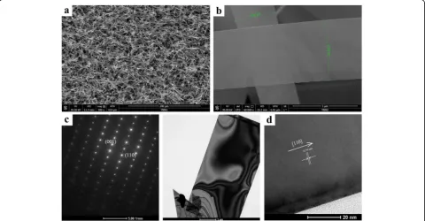
Figure2a shows a SEM image of the as-prepared CdSSe NBs. It is found that the CdSSe NBs have good morph-ology and uniform width and lengths up to hundreds of micrometers. Figure 2b is a high magnification SEM
Fig. 1A schematic diagram of the detector configuration
[image:2.595.56.291.88.236.2] [image:2.595.58.539.463.713.2]image of the CdSSe nanobelts. It is observed that the nanobelt is thin and uniform with 2.632 μm in width. Figure 2c and its inset present the TEM bright-field image and selected-area diffraction (SAD) pattern of a single nanobelt with a width of 2.94μm and thickness of less than 50 nm. The SAD pattern confirms the single-crystal quality, and it can be indexed to a hex-agonal structure with lattice parameters a= 4.177 Å and c= 6.776 Å. The corresponding HRTEM image is dis-played in Fig. 2d, and the lattice spacing between adja-cent plane is 0.34 nm, corresponding to the (110) crystal plane. Accordingly, its growth direction is along [110].
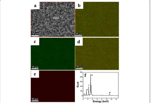
EDX and mapping of the CdSSe nanobelts are shown in Fig. 3. SEM image of a sample at low mul-tiples is displayed in Fig. 3a. It is observed that the entire region is covered with nanobelts. Figure 3b is the total distributions of Cd, S, and Se. The mappings of Cd, S, and Se elements are depicted in Fig. 3c–e, respectively. It revealed that Cd, S, and Se are uni-formly distributed in the whole nanobelts. EDX spectrum collected from the same nanobelts is pre-sented in Fig. 3f, indicating that the nanobelt is com-posed of Cd, S, and Se elements.
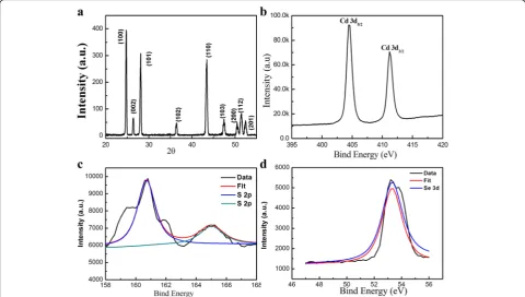
XRD and XPS pattern of CdSSe NBs are presented in Fig. 4. All diffraction peaks can be indexed to a hex-agonal structure of CdS0.76Se0.24 with lattice parameters a= 4.177 Å andc= 6.776 Å, which is consistent with the standard card (JCPDS no. 49-1459). The positions of the diffraction peaks (2θ= 24.72°, 26.35°, 28.13°, 36.42°, 43.47°, 47.5°, 50.4°, 51.4°, and 52.4°) matched with the crystal plane (100), (002), (101), (102), (110), (103), (200), (112), and (201), respectively. No other impurities are detected. The sharp and narrow diffraction peaks re-vealed that the obtained CdSSe nanobelts have good crystallinity. Figure 4b shows the binding energies of Cd3d5/2 and Cd3d3/2 for the CdSSe NBs at 404.8 and 411.7 eV, respectively, which are close to the values reported in the previous work [26]. The separation distance between two peaks is 6.9 eV, indicating that Cd atoms are in the complete CdS phase [27]. The deconvo-lution of the S(2p) peak shows two Gaussian peaks, cen-tered at 160.7 and 165.1 eV in Fig. 4c. The valence electron spectra of Se(3d) is depicted in Fig.4d, in which only one peak located at 53.5 eV was observed. There-fore, the XPS results confirm that the nanobelts are composed of Cd, S, and Se elements.
[image:3.595.57.542.384.713.2]Figure5is the photoluminescence spectrum of CdSSe nanobelts; there are two peaks in the range of 500– 1000 nm. One is centered at 603 nm originated from the near-band-edge (NBE) emission of the CdSSe nanobelts. The other centered at ~ 950 nm may be related to deep-level emission, which is observed in In2Se3 and Ga2Se3[28,29].
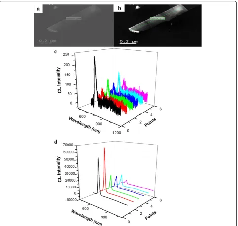
SEM and CL images of the single CdSSe nanobelt are described in Fig. 6a, b. It elucidated that the surface of the nanobelts is flat and smooth and the brightness is heterogeneous along its length. Figure6c, d is the spatial
resolution CL spectra of the same nanobelt at room temperature (295 K) and low temperature (93 K). It highlighted that the CL intensities of the characteristic NBE on CdSSe NB are different from point to point, and their signal noise ratio is not good at 295 K, whereas the CLs are strong with different intensities from point to point at 93 K. This result is in good agreement with the CL image. In addition, the characteristic peak is located at 625 nm, no defect emission is observed, and the in-tensity at 93 K is about 220-fold stronger than that at 295 K. Therefore, the CdSSe NB has good luminescent properties at low temperature.
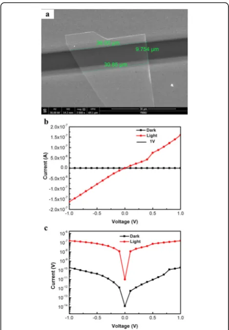
Figure7a is the SEM image of the nanodevice, which visualized that the CdSSe NB is not uniform in width. The widths of the measured NB are 30.85 and 36 μm and the length is 9.754μm, as marked in Fig.7a. TheI– Vcharacteristics of the CdSSe NB device is exhibited in Fig. 7b under dark conditions and white light illumin-ation with power density of 43.14 mW/cm2. As can be seen, the photocurrent increases greatly under the white light irradiation, because the incident light produces electron-hole pairs, thus improving the photocurrent. The linear shape ofI–Vcurve indicated that good ohmic contacts between the CdSSe NB and Ti/Au electrodes were formed. The photocurrent is 1.6×10⁻⁷A, and the dark current is about 1.96×10⁻¹⁰A. Therefore, the ratio of photocurrent to dark current is 816. Figure 7c is the
Fig. 5The PL emission spectra of CdSSe NBs
Fig. 4XRD patterns and XPS spectra of the CdSSe NBs.aXRD.bXPS spectrum of superposed Cd(3d).cHigh-resolution XPS spectrum for S(2p).
[image:4.595.57.538.89.361.2]I–V curve obtained after taking logarithm and found that the photocurrent is higher by three orders of mag-nitude than its dark current.
To further explore the photoelectronic properties of the devices, we measured the photocurrent of a single CdSSe NB device, as shown in Fig.8. At an applied bias-ing voltage of 1 V, the spectral response of the device in the range of 600 to 800 nm is displayed in Fig.8a. It is seen that the response is very strong as the wavelength is less than 674 nm, and then becomes weaker and weaker when the wavelength is more than 674 nm. Fig-ure 8b presents the measured I–Vcurve under illumin-ation of 674 nm light with different power densities. It is
found that the photocurrent increases with increasing power density, implying that the photogenerated carrier efficiency is proportional to the number of absorbed photons [30]. The logarithmic plot corresponding to Fig. 8b is highlighted in Fig. 8c. It revealed that the CdSSe NB device has the best response at a power dens-ity of 6.11 mW/cm2. Figure 8d is the relationship be-tween the photocurrent and the optical power density. By fitting the power density-dependent photocurrent value of Ip=APθ, where Ip is the photocurrent,P is the optical power density, A is the wavelength-dependent constant, the exponent θ determines the photocurrent response with power [31], a good fit of the experimental
[image:5.595.58.542.86.544.2]results has been obtained with θ= 0.69. Reports on a non-unity exponent with 0.5 < θ< 1 suggest a complex process of electron–hole generation, recombination, and trapping within the photoactive material [32], whereas the intensity dependence with θ < 0.5 may arise owing to defect mechanisms, including both recombination centers and traps. Therefore,θ= 0.69 means that CdSSe nanobelt has no defects, which is in agreement with that by HRTEM and CL.
It is well known that the spectral responsivity (Rλ) and
external quantum efficiency (EQE) are critical parame-ters for optical devices, which can be defined asRλ=Iph/
(PλS)and EQE =hcRλ/(qλ), whereIphis the difference be-tween the photocurrent and dark current,Pλis the light
power density irradiated on the nanobelt,Sis the effect-ive illuminated area, c is the velocity of light, h is the Planck’s constant,qis the electronic charge, andλis the exciting wavelength [33, 34]. We calculated the corre-spondingRλand EQE values of the CdSSe NB device are
10.4 A/W and 19.1%.
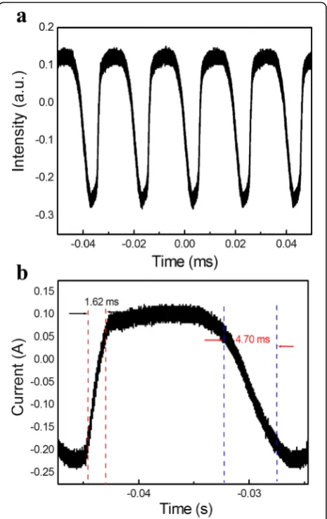
Figure 9a shows the time response of the CdSSe NB detector, which is measured by periodically turning on and off the 674-nm light with an intensity of 4.87 mW/ cm2at a bias voltage of 1 V. From that, we can see that CdSSe NB device exhibits a good reversible stability on switching properties. Figure 9b is the voltage rise and decay edge of a resistant measured by the oscilloscope. It reflects the photoconductance rise time and decay time of CdSSe NB. With and without illumination of 674-nm light (4.87 mW/cm2), the voltage of the resistant changes varies. It is seen that the rise/decay time is 1.62/ 4.70 ms, respectively. We compared important
Fig. 7SEM image andI–Vcurves of a single CdSSe NB detector.aSEM.b
I–Vcurves under dark conditions and white light illumination with power density of 43.14 mW/cm2.cI–Vgraph obtained after taking logarithm
[image:6.595.56.291.86.423.2] [image:6.595.61.539.471.694.2]parameters of our photodetector with those of others based on single nanobelt or nanosheet (NS). It is found that theRλof the CdSSe NB device in this work is larger
than that of other nanostructure photodetectors such as CdS [34] and ZnS NB [35], BiO2Se [36], GaSe [37], SnS [38], and Bi2S2NS [39]. The decay time is shorter than that of ZnS NB [35] and GaSe NS [37], but longer than that of others [34,36,38,39], as summarized in Table1, thus confirming the potential application of the CdSSe NB for photodetective field.
Conclusions
In summary, CdSSe NBs were grown in a high-temperature furnace by thermal evaporation. The obtained nanobelts were characterized by various methods. It is found that the CdSSe NBs have perfect microstructure without any defects and the nanobelts are composed of Cd, Se, and S elements. The CL results revealed that the intensity of single CdSSe nanobelt at low temperature (93 K) is stronger than that at room temperature (295 K), and the signal noise ratio is better at 93 K. After that, we developed the CdSSe photo-detector based on single NB and studied its optoelec-tronic properties. The detector achieved high performance with responsivity of 10.4 A/W, rise/decay time of 1.62/4.70 ms, and the external quantum effi-ciency (EQE) of 19.1% at 674 nm, which has good stabil-ity and repeatabilstabil-ity in the photoelectronic properties. This work paves the way towards for developing continuous-wavelength visible photodetector by tuning its composition.
Abbreviations
CL:Cathodoluminescence; EDX: Energy-dispersive X-ray; EQE: External quantum efficiency; HRTEM: High-resolution electron microscopy; NB: Nanobelt; NBE: Near-band-edge; NS: Nanosheet; PL: Photoluminescence; Rλ: Responsivity; SAD: Selected-area diffraction; SEM: Scanning electron microscopy (SEM); TEM: Transmission electron microscopy; XPS: X-ray photoelectron spectroscopy; XRD: X-ray diffraction
Funding
This work was supported by the National Natural Science Foundation of China (Grant No. 11764046, 11304275, and 61564010), Applied Basic Research Foundation of Yunnan Province (2017FB009), and Innovative Talents of Science and Technology Plan Projects of Yunnan Province (2014HB010).
Availability of Data and Materials
All data are fully available without restriction.
Authors’Contributions
YL guided the experiments and test process and revised the paper. LX carried out the synthesis of nanobelts and photoconductance measurement and prepared the manuscript. XF and QT carried out the characterization. QW analyzed the data. All authors read and approved the final manuscript.
Ethics Approval and Consent to Participate
Not applicable
Competing Interests
The authors declare that they have no competing interests.
[image:7.595.58.291.87.457.2]Fig. 9Current–time properties of single CdSSe NB photodetector upon 674-nm light illumination with 4.87 mW/cm2power density under 1 V bias.aI–tcharacteristics with on/off switching.bThe voltage rise and decay edge of a pulse response
Table 1Comparisons of important parameters of
photodetectors based on single different nanobelt/nanosheet
Materials Contact type
Response range
Responsivity Decay time
Ref
Cds NB OC < 500 nm 6 20μs [34]
ZnS NB SC UV ~ 2 < 0.3 s [35]
BiO2Se NS
OC 808 nm 6.5 2.8 ms [36]
GaSe NS SC 800 nm 3.5 0.1 s [37]
SnS2NS OC Visible 8.8 × 10⁻³ 5μs [38]
Bi2S3NS OC Visible-NIR 4.4 10μs [39]
CdSSe NB
OC 674 nm 10.4 4.7 ms This
work
[image:7.595.56.292.577.714.2]Publisher’s Note
Springer Nature remains neutral with regard to jurisdictional claims in published maps and institutional affiliations.
Author details
1Institute of Physics and Electronic Information, Yunnan Normal University,
Kunming 650500, People’s Republic of China.2Yunnan Key Laboratory of Opto-electronic Information Technology, Kunming 650500, People’s Republic of China.3Key Laboratory of Yunnan Higher Education Institutes for Optoelectric Information Technology, Kunming 650500, People’s Republic of China.
Received: 26 April 2018 Accepted: 30 May 2018
References
1. Steckel JS, Coe-Sullivan S, Bulovic Bawendi MG (2003) 1.3μm to 1.55μm tunable electroluminescence from PbSe quantum dots embedded within an organic device. Adv. Mater 15(21):1862–1866
2. Zhao J, Baardecker JA, Munro AM, Liu MS (2008) Efficient CdSe/CdS quantum dot light-emitting diodes using a thermally polymerized hole transport layer. Nano Lett 6(3):463
3. Li FZ, Luo LB, Yang QD, Wu D, Xie C, Nie B, Jie JS, Wu CY, Wang L, Yu SH (2013) Ultrahigh mobility of p-type CdS nanowires: surface charge transfer doping and photovoltaic devices. Adv. Energy Mater. 3:579
4. Khosroabadi S, Keshmiri SH (2014) Design of a high efficiency ultrathin CdS/ CdTe solar cell using back surface field and backside distributed Bragg reflector. Opt. Express 22:921–929
5. Yu P, Wu J, Liu S, Xiong J, Jagadish J, Wang ZM (2016) Design and fabrication of silicon nanowires towards efficient solar cells. Nano Today 11:704–737 6. Tong X, Zhou Y, Jin L, Basu K, Adhikari R, Selopal GS, Tong X, Zhao H, Sun S,
Vomiero A, Wang ZM, Rosei F (2017) Heavy metal-free, near-infrared colloidal quantum dots for efficient photoelectrochemical hydrogen generation. Nano Energy 31:441–449
7. Zhao Z, Qin F, Kasiraju S, Xie L, Alam MK, Chen S, Wang D, Ren Z, Wang Z, Grabow LC, Bao J (2017) Vertically aligned MoS2/Mo2C hybrid nanosheets
grown on carbon paper for efficient electrocatalytic hydrogen evolution. ACS Catalysis 7:7312–7318
8. Rath AK, Bernechea M, Martinez L, Konstantatos G (2011) Solution-processed heterojunction solar cells based on p-type PbS quantum dots and n-type Bi2S3nanocrystals. Adv. Mater. 23:3712
9. Shafa M, Ji H, Gao L, Yu P, Ding Q, Zhou Z, Li H, Niu XB, Wu J, Wang ZM (2016) Mid-infrared photodetectors based on InSb micro/nanostructures grown on low-cost mica substrates. Materials Lett 169:77–81
10. Liu YK, Zhou XP, Hou DD, Wu H (2006) The photoconductance of a single CdS nanoribbon. J. Mater. Sci. 41:6492–6496
11. Nie B, Hu JG, Luo LB, Xie C, Zeng LH, Lv P, Li FZ et al (2013) Monolayer graphene film on ZnO nanorod array for high-performance Schottky junction ultraviolet photodetectors. Small 9:2872–2879
12. Kung SC, Ver der Veer WE, Yang F, Donavan KC (2010) 20μs photocurrent response from lithographically patterned nanocrystalline cadmium selenide nanowires. Nano Lett. 10:1481–1485
13. Xu S, Qin Y, Xu C, Wei YG, Yang RS, Wang ZL (2010) Self-powered nanowire devices. Nat. Nanotech. 5:366–373
14. Fang XS, Bando Y, Liao MY, Gautam UK (2009) Single-crystalline ZnS nanobelts as ultraviolet-light sensors. Adv. Mater. 21:2034–2039 15. An QW, Meng XQ (2016) Aligned arrays of CdS nanotubes for
high-performance fully nanostructured photodetector with higher photosensitivity. J. Mater. Sci. 27:11952–11960
16. Wu YM, Zhang H, Liu YK, Chen WW, Ma J (2015) Synthesis and gas sensing properties of single La-doped SnO2nanobelt. Sensor 15:14230–14240
17. Yang SZ, Wang LF, Tian XZ, Xu Z, Wang ZL (2012) The piezotronic effect of zinc oxide nanowires studied by in situ TEM. Adv. Mater. 24(34):4676–4682 18. Hou DD, Liu YK, Yu DP (2015) Multicolor photodetector of a single Er3
+-doped CdS nanoribbon. Nanoscale Res. Lett. 10:285
19. Nusir AI, Aguilar J, Bever Z, Manasreh MO (2014) Uncooled photodetectors based on CdSe nanocrystals with an interdigital metallization. Appl. Phys. Lett. 104:051124
20. Sanchez OL, Lembke D, Kayci M, Radenovic A, Kis A (2013) Ultrasensitive photodetectors based on monolayer MoS2. Nat. Nanotechnol. 8:497–501
21. Liu Y, Zapien JA, Shan YY, Geng CY, Lee CY (2005) Wavelength-controlled lasing in ZnxCd1–xS single-crystal nanoribbons. Adv. Mater. 17:1372
22. Yoon YJ, Park KS, Heo JH, Park JG (2010) Synthesis of ZnxCd1-xSe (0≤x≤1)
alloyed nanowires for variable-wavelength photodetectors. J. Mater. Chem. 20(12):2386–2390
23. Wang L, Wang XE, Chen R, Wu CY, Yu YQ, Xu J, Hu JG, Luo LB et al (2014) Gallium dopedn-type ZnxCd1-xS nanoribbons: synthesis and
photoconductivity properties. J. Appl. Phys. 115:063108
24. Guo PF, Hu W, Zhang QL, Zhang XJ, Zhu XL (2014) Semiconductor alloy nanoribbon lateral heterostructures for high-performance photodetectors. Adv. Mater. 26:2844–2849
25. Chen C, Qin Z, Liu Y, Zhang Y, Li Y, Shen S, Wang ZM, Song HZ (2017) Promotion on acetone sensing of single SnO2nanobelt by Eu doping.
Nanoscale Res. Lett. 12:405
26. Chen S, Zhang X, Zhang Q, Tan W (2009) Trioctylphosphine as both solvent and stabilizer to synthesize CdS nanorods. Nanoscale Res. Lett. 4:1159–1165 27. Baghchesara MA, Yousefi R, Cheraghizade M, Sheini FJ (2016) Photocurrent
application of Zn-doped CdS nanostructures grown by thermal evaporation method. Ceramics International 42:1892–1896
28. Okamoto T, Yamada A, Konagai M (1997) Growth and characterization of In2Se3 epitaxial films by molecular beam epitaxy. J. Cry. Growth 175/176: 1045–1050
29. Okamoto T, Yamada A, Konagai M, Takahashi K (1994) Polarized photoluminescence in vacancy-ordered Ga2Se3. J. Cry. Growth 138:204–207
30. Chen G, Yu Y, Zheng K (2015) Fabrication of ultrathin Bi2S3 nanosheets for high-performance, flexible, visible-NIR photodetectors. Small 11(24):2848–2855 31. Yang SX, Tongay S, Li Y (2014) Layer-dependent electrical and optoelectronic
responses of ReSe2 nanosheet transistors. Nanoscale 6(13):7226–7231 32. Hussain AA, Sharma B, Barman T, Pal AR (2016) Self-powered broadband
photodetector using plasmonic titanium nitride. ACS Appl. Mater. Interf. 8: 4258–4265
33. Kung SC, Xing WD, Veer WE (2011) Tunable photoconduction sensitivity and bandwidth for lithographically patterned nanocrystalline cadmium selenide nanowires. ACS Nano 5(9):7627–7639
34. Li L, Wu PC, Fang XS (2010) Single-crystalline CdS nanobelts for excellent field-emitters and ultrahigh quantum-efficiency photodetectors. Adv. Mater. 22:3161–3165
35. Zhai TY, Li L, Wang X, Fang XS, Bando Y, Golberg D (2010) Recent developments in one-dimensional inorganic nanostructures for photodetectors. Adv. Funct. Mater. 20:4233
36. Li J, Wang ZX, Wen Y, Chu JW, Yin L, Cheng RQ, Lei L, He P, Jiang C, Feng LP, He J (2018) High-performance near-infrared photodetector based on ultrathin Bi2O2Se nanosheets. Adv. Funct. Mater. 28:1706437
37. Mukherjee B, Cai Y, Tan HR, Feng YP, Tok ES, Sow CH (2013) NIR schottky photodetectors based on individual single-crystalline GeSe nanosheet. ACS Appl. Mater. Interfaces 5:9594
38. Chen G, Yu Y, Zheng K, Ding T, Wang W, Jiang Y, Yang Q (2015) Fabrication of ultrathin Bi2S3 nanosheets for high-performance, flexible, visible–NIR photodetectors. Small 11:2848
39. Su G, Hadjiev VG, Loya PE, Zhang J, Lei S, Maharjan S, Dong P, Lou J, Peng H (2015) Fabrication of ultrathin Bi2S3nanosheets for high-performance,