REVIEW
Deformable devices with integrated
functional nanomaterials for wearable
electronics
Jaemin Kim
1,2†, Jongsu Lee
1,2†, Donghee Son
1,2, Moon Kee Choi
1,2and Dae‑Hyeong Kim
1,2*Abstract
As the market and related industry for wearable electronics dramatically expands, there are continuous and strong
demands for flexible and stretchable devices to be seamlessly integrated with soft and curvilinear human skin or
clothes. However, the mechanical mismatch between the rigid conventional electronics and the soft human body
causes many problems. Therefore, various prospective nanomaterials that possess a much lower flexural rigidity than
their bulk counterparts have rapidly established themselves as promising electronic materials replacing rigid silicon
and/or compound semiconductors in next‑generation wearable devices. Many hybrid structures of multiple nanoma‑
terials have been also developed to pursue both high performance and multifunctionality. Here, we provide an over‑
view of state‑of‑the‑art wearable devices based on one‑ or two‑dimensional nanomaterials (e.g., carbon nanotubes,
graphene, single‑crystal silicon and oxide nanomembranes, organic nanomaterials and their hybrids) in combination
with zero‑dimensional functional nanomaterials (e.g., metal/oxide nanoparticles and quantum dots). Starting from an
introduction of materials strategies, we describe device designs and the roles of individual ones in integrated sys‑
tems. Detailed application examples of wearable sensors/actuators, memories, energy devices, and displays are also
presented.
Keywords:
Silicon nanomembrane, Functional nanomaterials, Flexible electronics, Stretchable electronics,
Wearable electronics
© 2016 Kim et al. This article is distributed under the terms of the Creative Commons Attribution 4.0 International License (http:// creativecommons.org/licenses/by/4.0/), which permits unrestricted use, distribution, and reproduction in any medium, provided you give appropriate credit to the original author(s) and the source, provide a link to the Creative Commons license, and indicate if changes were made.
1 Introduction
In the rapid technology development of low-power
sili-con electronics, light-emitting diodes (LEDs) fabricated
on unconventionally shaped substrates, high-capacity
lithium-ion batteries, and various wearable electronic
devices such as smart glasses, watches, and lenses have
been unveiled both in academic journals and on the
mar-ket. In spite of their superb performance, wearable form
factors, and compact sizes, challenges remain mainly
owing to their large thickness and mechanical
rigid-ity, which result in a mechanical mismatch between the
device and the skin, and thereby discomfort, a low
sig-nal-to-noise ratio, and measurement errors [
1
]. In this
regard, achieving mechanical deformability of the
wear-able electronic/optoelectronic devices while maintaining
high performances has been a major research goal [
2
–
6
].
One promising strategy is to replace the rigid
elec-tronic materials (e.g., silicon wafer) with flexible
nano-materials (e.g., silicon nanomembrane (SiNM) [
7
–
11
],
carbon nanotubes (CNTs) [
12
–
14
], graphene (GP) [
1
,
15
,
16
], and organic nanomaterials [
17
,
18
]). The
elec-tronic properties of the SiNM (down to tens of
nanom-eters) remain the same as the bulk silicon wafer [
19
],
but its bendability dramatically increases owing to the
reduced thickness [
5
]. SiNM-based devices outperform
their competitors including low-temperature
polycrys-talline silicon (LTPS) and organic devices by virtue of
their high electron mobility [
20
]. However, SiNM based
device might have issues in the high cost and
compli-cated fabrication processes. Meanwhile, carbon
nano-materials (e.g., CNTs and GP) [
21
,
22
] have been getting
Open Access
*Correspondence: [email protected]
attentions as next-generation semiconducting
nanomate-rials. The mobility of single-walled CNTs (SWNTs) and
exfoliated GP have been reported up to 100,000 [
21
] and
230,000 cm
2V
−1s
−1[
22
], respectively, which are higher
than that of single-crystal silicon. Their ultrathin
thick-ness enables them to be seamlessly integrated in
wear-able devices while achieving the transparency [
23
–
25
].
The mass production, device performance, and
fabri-cation processes of these carbon nanomaterials,
how-ever, have many remaining challenges for commercial
device applications [
26
]. Organic nanomaterials such
as organic nanowires/nanofibers also have recently
uti-lized as electric materials for fabricating complementary
metal–oxide–semiconductor (CMOS) circuits [
27
] and
wearable power generators [
28
,
29
]. Intrinsic
deform-ability of organic nanomaterials, solution processdeform-ability,
and low cost make them promising for wearable devices
[
27
]. However, their low electrical performances should
be resolved for its widespread applications [
17
].
Another approach to achieve both high performance
and multifunctionality is to utilize hybrids of
nanoma-terials [
30
–
36
]. Functional hybrid nanomaterials often
exhibit substantially different physical, mechanical,
mag-netic, chemical, and optical properties compared to their
individual and/or bulk counterparts [
37
–
40
]. By
integrat-ing different functional nanomaterials, the performance
of wearable devices can be dramatically improved and/or
diversified [
1
,
7
,
41
–
46
]. For the realization of this goal,
the type, size, thickness, and concentration of the
nano-materials should be carefully designed [
46
]. In the
follow-ing, we summarize recently reported wearable sensors/
actuators [
7
,
13
,
47
], memories [
41
,
48
], energy storage
devices [
49
], and displays [
50
,
51
] that exploit various
nanomaterials [
7
,
44
,
46
,
52
,
53
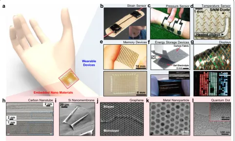
] and their hybrids (Fig.
1
).
We also describe the roles of each nanomaterial in
spe-cific devices, improved device functions, their system
integrations, and provide brief perspectives on future
research directions.
2 Review
2.1 Wearable sensors/actuators
Wearable sensors/actuators have recently attracted
con-siderable interest because of their mobile healthcare [
54
]
and virtual reality applications [
55
]. Sensors/actuators
worn on the body, in particular, have drawn attention for
the continuous and accurate monitoring of
physiologi-cal (e.g., motion [
1
,
47
] and temperature [
56
,
57
]) and
electrophysiological (e.g., electrocardiograms [
58
,
59
]
and electromyograms [
60
,
61
]) signals and appropriate
instant feedback on them [
1
], which are important for
point-of-care medical diagnostics and therapy. This
sec-tion describes representative wearable sensors/actuators
based on functional nanomaterials and their application
examples in healthcare and human–machine interfaces.
2.1.1 SiNM‑based sensors
Deformability, which is one of the key characteristics of
wearable electronics, can be achieved by making
inor-ganic materials (i.e., silicon) as thin as possible, down
to the nanometer scale (i.e., nanomembrane) [
5
]. SiNM
can be fabricated through several processes. One easy
fabrication method is to remove the buried oxide of a
silicon-on-insulator (SOI) wafer and pick the top part
up or to etch the bottom silicon of the SOI wafer and use
the remaining top part [
7
]. The obtained SiNM can be
located in the desired position of the designed layout by
using previously reported transfer printing techniques.
SiNM maintains the high carrier mobility [
20
] and
intrin-sic piezoresistivity [
7
] of the bulk monocrystalline
sili-con, while having a high flexibility, which enables diverse
wearable electronics applications.
For instance, multiplexing through SiNM transistors
integrated into the flexible high-density electrode array
achieves the real-time analysis of
electrophysiologi-cal signals over a large area of the brain [
10
] and heart
[
62
] surface. SiNM strain gauges integrated onto
poly-meric substrates are applied as wearable motion
sen-sors thanks to their high piezoresistive sensitivity [
7
,
8
].
Figure
2
a shows images of a SiNM strain gauge array
integrated with a finger tube that conforms to the thumb.
The bending motion of the thumb applies a tensile stress
to the SiNM strain gauges, and their resistance increases
accordingly without any hysteresis (Fig.
2
b). Multiplexing
by SiNM p–i–n junction diodes is also advantageous for
constructing a wearable high-spatial-resolution
tempera-ture sensor array. Figure
2
c depicts an 8
×
8 p–i–n
junc-tion diode array located on a heated Cu element (left) and
its measured temperature distribution (right). The
recti-fying characteristics of silicon diodes enable each cell to
be individually addressable with the minimum number of
wires and crosstalk, achieving a high spatial resolution.
The ultrathin dimensions of the sensor array facilitate not
only conformal contacts with the target surface but also a
fast response time by virtue of its extremely low thermal
mass.
mounted on the prosthetic skin distinguishes different
surface temperatures (Fig.
2
f). Although these SiNM
sen-sors exhibit a high potential for various wearable sensing
applications, there are cost issues to be addressed for the
development of commercial products.
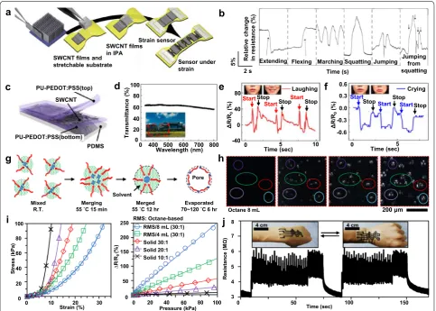
2.1.2 CNT‑based wearable sensors
The macroscopic form of CNTs in most devices is either
their aligned arrays or random networks. Hata et al. [
12
]
developed a synthesis method for ultra-long vertically
aligned CNTs using the water-assisted chemical vapor
deposition (CVD) process. The vertically aligned CNTs
could be selectively grown on a patterned catalyst layer
and transferred onto a stretchable substrate for device
applications such as a strain sensor (Fig.
3
a) [
13
]. In
this strain measurement, the CNT film deforms as the
substrate is stretched and its resistance increases. This
relative change in the resistance according to the applied
strain can be used for human-motion detection. When
the sensor is attached to a human knee, the change in the
resistance exhibits variations corresponding to the
wear-er’s motion (Fig.
3
b). Although vertical CNTs are densely
aligned similar to a forest and therefore have a dark color,
randomly oriented CNT networks are relatively
trans-parent, particularly at reduced CNT concentrations [
14
].
Figure
3
c shows a schematic of a transparent patch-type
strain sensor using random-network CNTs integrated
with a conducting polymer. By virtue of its optical
trans-parency (62 %), it was inconspicuously patched onto a
human face and successfully distinguished facial motions
(Fig.
3
d–f).
CNTs are also excellent nanoscale filler materials
owing to their small size with good dispersion and
excep-tional electrical and physical properties [
63
,
64
]. In this
Memory Devices
10 nm
Strain Sensor Pressure Sensor
a
b
c
d
Heated object 1 mm SiNM Diode
Temperature Sensor
f
Energy Storage Devicesg
Displaysh
Carbon Nanotubei
Si Nanomembranej
Graphenek
Metal Nanoparticlel
Quantum DotEmbedded Nano Materials
Wearable Devices
1 cm
2 nm
2 nm 1 nm
20 μm Bilayer
Monolayer
10 mm
6 mm
e
regard, electrically conductive rubber (ECR), which is
a composite of CNTs and elastomeric polymers, is
pre-pared and used for a wearable mechanical sensor [
47
]. To
enhance the sensitivity, nanopores and micropores are
introduced into the ECR, thereby increasing its
piezore-sistivity and maximizing the locally induced strain when
deformed [
47
]. Figure
3
g shows a representative method
for introducing pores with a uniform size and
distribu-tion in the ECR. The key idea of this method is to use a
reverse micelle solution (RMS) comprising an emulsifier,
deionized (DI) water, and an organic solvent. In
accord-ance with careful sequential heat treatments, the
migra-tion and merging of the reverse micelles and subsequent
pore generations occur (Fig.
3
h). A larger porosity and
lower elastic modulus are achieved if a larger amount
of solvent is included in the RMS, thereby resulting in a
higher pressure sensitivity (Fig.
3
i). An ECR-based strain
gauge fabricated on a medical bandage by using ink-jet
printing forms a conformal contact with the human wrist
and successfully monitors wrist motions. Although
sen-sors based on CNT networks/composites are relatively
cheap, especially those that are solution-processed, and
mechanically compatible when worn on the human body,
several issues such as a slow response time, a large area
uniformity, and the hysteresis and drift of signals still
need to be solved.
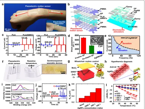
2.1.3 Wearable sensors/actuators based on nanomaterial
hybrids
In several cases, electronic materials having a relatively
poor performance are incorporated owing to the
lim-ited processing temperature and chemical/mechanical
22.6 22.4 22.2 22.0 21.8 21.6 Temp. (˚C)
c
2 mmb
Bending cycles
Rel.
resi
st.
change
0.08 0.06 0.04 0.02 0.00 I
II
I I
II II I bend motion
side-to-side motion
15
0 5 10 ΔR/R0
(%)
d
Bend Bend Fist250
ΔR (Ω
) 200
150 100 50 0
e
Typing0 10 20 30 40 50 60 70
Time (s)
0 10 20 30 40 50 60 70
Time (s) 0
50 100 150 200 250 300 350
ΔR (Ω
)
Grasp Maintain
Relax Grasping
0.8 1.0 1.2
1.4 Te
mp. (˚
C)
0 5 10 15 20 25
Time (s)
0 300 600 900 1200 1500 1800 IR Sensor Temp. Sens.
f
Current
(μ
A
)
3 cm
Cold
Current
(μ
A)
1.0 1.5 2.0 2.5 3.0 3.5 4.0
Time (s)
0 300 600 900 1200 1500 180020 30 40 50 60 70 IR Sensor Temp. Sens. Te
mp
. (˚C)
Keyboard
Baseball 2 cm
10 cm
5 cm
a
resistance of plastic substrates [
65
]. Appropriately
cho-sen functional nanomaterials compensate for these
limi-tations and improve the device performance [
46
,
66
].
Figure
4
a shows a transparent piezoelectric motion
sen-sor and electrotactile stimulator (inset) conformally
lami-nated onto the human skin. The piezoelectric motion
sensor consists of GP layers as the transparent electrodes,
polylactic acid (PLA) as the piezoelectric material, and
SWNTs as the piezoelectric performance enhancer
(Fig.
4
b, left). Moreover, the electrotactile stimulator
uti-lizes doped GP layers as transparent electrodes and silver
nanowires (AgNWs) as a conductivity enhancer (Fig.
4
b,
right). The strain-induced charge separation in PLA is
the main mechanism for piezoelectric energy generation.
The local increase in the modulus by the CNTs increases
the locally induced strain inside PLA under deformation,
which maximizes charge generation (Fig.
4
c). Figure
4
d
shows the conductivity enhancement by AgNWs
sand-wiched between GP layers. The enhanced conductivity of
the GP/AgNWs/GP hybrid contributes to effective
elec-trotactile stimulation (Fig.
4
e).
Figure
4
f shows an illustration and optical image
(inset) of a semitransparent piezoelectric strain sensor
and resistive temperature sensor for measuring wrist
motions and body-temperature changes for wheelchair
control and hypothermia diagnosis, respectively. The
Extending Flexing Marching Squatting Jumping Jumping from
squatting
Relativ
e
change
in
res
ista
nc
e (%
)
5%
2 s Time (s)
a
SWCNT films and stretchable substrate
SWCNT films in IPA
Strain sensor
Sensor under strain
PU-PEDOT:PSS(top) SWCNT
PU-PEDOT:PSS(bottom) PDMS
b
c
d
f
g
Mixed
R.T. 55 ˚C 15 minMerging 55 ˚C 12 hrMerged 70~120 ˚C 6 hrEvaporated
Pore
Solvent
h
Octane 8 mL 200 μm
150 100
50 0
8
7
6
4 5
3
Resistance
(M
Ω)
Time (sec)
4 cm 4 cm
i
Strain (%)
Stress
(kPa)
0 10 20 30
100
20
0 40 60 80
Pressure (kPa) 250
200
150
100
50
0
0 20 40 60 80
∆R
/R0
(%
)
RMS/8 mL (30:1) RMS/4 mL (30:1) Solid 30:1 Solid 20:1 Solid 10:1 RMS: Octane-based
100
j
Wavelength (nm) 400 500 600 700 0
20
800 0
40 60 80 100
Tr
ansmittance
(%
)
Time (sec)5
-40 0 10
0 40 80
ΔR/R
0
(%
)
e
Time (sec)5
-0.6 0 -0.3
0.0 0.3 0.6
ΔR/R
0
(%
)
Laughing Crying
StartStop
StartStopStartStop StartStopStartStopStartStop
strain sensor consists of a ZnO nanomembrane as the
piezoelectric material and SWNT networks as the
per-formance enhancer (Fig.
4
g). The temperature sensor
consists of silver nanoparticles (AgNPs) embedded in
the ZnO:Al (AZO) nanomembrane for improving its
sensitivity (Fig.
4
h). For the strain sensor,
co-depos-ited Cr and SWNTs layers improve the crystallinity
of ZnO and passivate intrinsic defects, respectively
(Fig.
4
i). These modifications dramatically amplify
the piezoelectric voltage output of the intrinsic ZnO
nanomembrane (Fig.
4
j). For the temperature sensor,
E
C– E
F(E
C, minimum energy of the conduction band;
E
F, Fermi energy level) is proportional to the
con-centration of AgNPs inside the ZnO nanomembrane
(Fig.
4
k). The high concentration of AgNPs increases
the carrier density and therefore improves the
sensitiv-ity of the temperature sensor (Fig.
4
l). A more in-depth
study of functional hybrid nanomaterials would
pro-vide new opportunities for high-performance wearable
devices.
b
Electrotactile stimulators Epoxy PMMA PLA/ SWNTs GP Piezoelectric motion sensor GP PMMA PDMS Epoxy GP /AgNW /GP 0 200 400 600 800 Sh eet resi stance (Ω /) AgNW GP 2 μm ZnO:Al AgNPsh
Hypothermia diagnosisg
Cr ZnO SWNT
MoOx
Wheelchair motion control
ITO PI
f
Piezoelectricstrain sensor temperature Resistive wearable devicesSemitransparent sensor
5 mm
l
R/R0 (%
)
Temperature (oC) 0
-10 -20
20 30 40 50 60
AZO
100:1 300:1
-30 1000:1 AgNP
ratio Pt
-40
AgNPs concentration (ratio)
k
EC -EF (eV) 0.2 0.4 0.6 0.8 90 750 mVj
ZnO 800 400 0 -400 Vo ltage (mV ) Time (s)0 30 60
Cr/ZnO
Cr/ZnO/SWNT
5 mV 60 mV
i
534 ( yti sn et nI a.u. )Binding energy (eV) 526 528 530 532 10000
15000 20000
OL OC
ZnO
ZnO/SWNT 10000
15000 20000
a
Piezoelectric motion sensorElectrotactile stimulator
50 mm 20 mm
0 10 20 30 40
-120-80 -400 40 80 120 0.5 nA 210 mV 44 mV
0 10 20 30 40
-3 -2 -10 1 2
3 PLA PLA/SWNTs
Time (sec) (t ner ru Cn A) Time (sec) Vo ltage (m V)
c
4 nA PLA PLA/SWNTs Frequency (Hz) Current (m A)e
No Sensation0 40 80 120
12 18 24 30 36 42 GP/AgNW/GP Sensation
d
PI ITO2.2 Wearable memories
Data recorded by wearable sensors should be either
transferred or stored for the analysis. Usually, the data are
stored in memory devices and retrieved when needed. In
this section, two types of ultrathin deformable
nonvola-tile memory devices—charge-trap floating-gate
mem-ory (CTFM) [
48
] and resistive random access memory
(RRAM) [
41
]—are described.
2.2.1 Deformable charge‑trap floating‑gate memory
Since the concept of memory devices using floating gates
was first proposed [
67
], field-effect transistor
(FET)-based CTFM has established itself as a dominant data
storage device owing to its small area and compatibility
with the CMOS process [
68
,
69
]. For the realization of
deformable CTFMs as next-generation devices, the rigid
active materials are replaced with deformable ones such
as organic materials [
70
,
71
], SWNTs [
48
], 2D
nanomem-branes [
72
], and even inorganic SiNMs [
73
]. Figure
5
a and
b show the device structure of an SWNT-based CTFM
and its laminated form on the human skin, respectively.
The Au nanomembrane as a floating gate maximizes the
charge capturing functionality (Fig.
5
c). Soft active layers
of SWNT networks are located at the neutral mechanical
plane and allow stable operation under deformation.
The floating gate of a continuous metal film has a
criti-cal limitation for the retention time [
74
]. Instead, metal
nanoparticles (NPs) are a promising candidate as the
floating gate to realize a fast program/erase speed and
long retention time [
74
]. Figure
5
e shows an optical image
of a fabricated flexible CTFM using poly(4-vinylphenol)
(PVP), pentacene, and gold nanoparticles (AuNPs) as the
dielectric, semiconductor, and charge-trap layer,
respec-tively. AuNPs are electrostatically adsorbed onto the PVP
blocking oxide, thereby forming a monolayer of AuNPs
(Fig.
5
f). A large on/off window (>10 V) is obtained
owing to the high density of AuNPs (Fig.
5
g).
Repeti-tive bending up to 1000 cycles with a bending radius of
20 mm does not diminish the performance of the CTFM.
2.2.2 Nanoparticle‑embedded wearable RRAM
RRAM is another promising candidate for future
non-volatile memory devices [
75
–
77
]. By integrating RRAM
with wearable sensors, a low power consumption and
mechanical deformability are important for long-term
use in mobile environments [
41
]. Figure
5
i shows
wear-able RRAM consisting of AuNP charge-trap layers
that reduce its operation current. Serpentine
intercon-nections make the wearable RRAM stretchable up to
25 % strain (Fig.
5
j–l). AuNPs embedded between TiO
2nanomembranes by Langmuir–Blodgett assembly form a
uniform layer over a large area (Fig.
5
m–o). The
opera-tion current of the wearable RRAM with one AuNP layer
is decreased by one order of magnitude compared to that
without AuNPs (Fig.
5
p). Three layers of AuNPs exhibit a
larger current decrease (by almost a factor of three).
2.3 Wearable displays
To construct user-interactive wearable electronic
sys-tems, deformable displays that visualize measured or
stored data are indispensable for users. Recently, several
breakthroughs in deformable LED technologies,
includ-ing deformable inorganic/organic LEDs [
51
,
78
–
81
],
polymer LEDs [
82
–
84
], and quantum-dot LEDs (QLEDs)
[
85
–
87
], have been reported.
Figure
6
a–c show an image of a deformable actively
multiplexed organic LED array, the device structure, and
the bending capability, respectively. However, organic
light-emitting materials have a low stability in air and a
low photostability, and thus they need thick
encapsula-tion under ambient condiencapsula-tions. Quantum dots, on the
other hand, have favorable properties such as a good
stability in air, good photostability, printability on
vari-ous substrates, and a high brightness at low operating
voltages, which are important key factors for
deform-able/wearable displays [
88
,
89
]. Figure
6
d and e show the
structure of recently reported wearable QLED devices
[
44
]. Thanks to ultrathin active and encapsulation
lay-ers, the total thickness of the device is ~ 2.6 μm, enabling
conformal contact with the wearer’s skin. The wearable
QLED is turned on at a low voltage (2 V; Fig.
6
j) and
endures 20 % stretching up to 1000 cycles without any
degradation in its brightness (Fig.
6
g). The use of
biocom-patible quantum dots and the replacement of the rigid
transparent electrodes with soft ones further improve the
practical applications of wearable QLEDs.
2.4 Wearable energy devices
Energy storage devices and power generators that supply
power to wearable electronics need flexibility and
bio-compatibility. An all-solid-state supercapacitor (SC) [
45
,
49
,
90
,
91
] is a suitable energy storage device with regard
to this point. Moreover, SCs have a high power density,
a fast charging/discharging speed, and cycle durability
[
92
]. In case of the wearable power generators, flexible
and soft fiber-based materials are suitable owing to the
requirement of high deformability [
28
]. In this section,
carbon-nanomaterial-based flexible SCs and organic
nanofiber-based power generators are reviewed.
2.4.1 CNT‑based wearable energy devices
random networks (Fig.
7
a, b) [
49
]. These engineered
fabric electrodes assembled with a fabric separator in
between form the SC (Fig.
7
c). The large surface area of
CNTs enables further decoration with other
nanomateri-als (e.g., pseudocapacitive metal oxide NPs such as MnO
2and RuO
2) [
94
,
95
]. The surface of the CNT fabric is
elec-troplated with MnO
2NPs (Fig.
7
d, e), which increases the
specific capacitance.
Instead of coating fabrics, carbon fibers are used to
make a woven fabric, which can be applied to flexible
textile electrodes [
45
]. To maximize the surface area,
ver-tically-aligned CNTs are additionally synthesized on the
carbon fabric. Electroplating vertical CNTs with RuO
2NPs further increases the capacitance (Fig.
7
f), and an
all-solid-state wearable SC is fabricated by sandwiching a
poly(vinyl alcohol) (PVA)-H
3PO
4gel electrolyte between
two modified carbon fabric electrodes (Fig.
7
g). The
resulting SC exhibits high performance up to 135-degree
bending and 4000 charge–discharge cycles (Fig.
7
h–j).
2.4.2 GP‑based wearable energy devices
to fabricate flexible carbon electrodes (Fig.
7
k). The
packing density (ρ) of the GP sheets can be controlled
by changing the ratio of the volatile and nonvolatile
liquids in the gel (Fig.
7
l, m). Figure
7
n and o show
the specific capacitance and volumetric capacitance,
respectively, of SCs using stacked GP electrodes for
different values of ρ. The specific capacitance slightly
decreases as ρ increases, whereas the volumetric
capacitance is nearly proportional to ρ. Although
most SCs made of activated carbon exhibit a
volu-metric energy density of 5–8 Wh/L, SCs made of the
GP assembly exhibit a volumetric energy density of
60 Wh/L, which is similar to that of lead-acid batteries
(50–90 Wh/L).
2.4.3 Organic nanofiber‑based wearable power generators
To harvest electrical energy from body movements,
piezoelectric nanogenerators (PENGs) and
triboelec-tric nanogenerators (TENGs) have been used [
28
,
96
].
Organic nanofibers such as polyvinylidene fluoride
(PVDF) formed by using electrospinning processes
have shown superb deformability as well as high
pie-zoresistivity, facilitating its use in wearable
applica-tions [
18
,
28
]. Piezoelectric power generation using a
single PVDF nanofiber [
97
], aligned multiple PVDF
nanofibers [
98
,
99
], and randomly distributed nanofiber
networks [
100
] have been demonstrated. Parallel and
series connection of PVDF nanofibers increase the
gen-erated voltage and current [
98
]. However, relatively low
output power of PENGs has limited the application for
wearable devices with high power consumption [
28
].
In contrast, TENGs have shown much higher output
power than PENGs [
28
]. Electrospun PVDF nanofibers
are also suitable for fabrication of the TENG because
of their strong electronegativity and high porous
mor-phology offering large contact area to increase the
out-put power [
28
,
101
]. The PVDF nanofiber-based TENG
has been recently demonstrated as wearable forms
[
28
]. Seamless integration of the organic
nanofiber-based wearable power generators with energy storage
devices and control circuits is another important future
research topic.
3 Conclusions
The mechanical, electrical, and optical properties of
bulk materials change as their size is reduced and/
or nanoscale structure engineering is introduced. By
using the unique properties of such nanomaterials or
their hybrids, many breakthroughs in wearable devices
have been accomplished. In this paper, we reviewed the
current status of wearable devices including sensors/
actuators, memory devices, displays, and energy
stor-age devices. We particularly focused on the use of
func-tional nanomaterials to enhancing the deformability and
performance of these devices. Continuous research and
development of new nanomaterials/hybrids and their
integration into variety of electronic/optoelectronic
devices would provide new opportunities for
next-gen-eration wearable electronics.
Authors’ contributions
JK and JL contributed equally. JK, JL, and D‑HK wrote the manuscript. JK, JL, DS, MKC and D‑HK designed the figures. All authors read and approved the final manuscript.
Author details
1 Center for Nanoparticle Research, Institute for Basic Science (IBS), Seoul 151‑742, Republic of Korea. 2 School of Chemical and Biological Engineering, Institute of Chemical Processes, Seoul National University, Seoul 151‑742, Republic of Korea.
Super Capacitor
Carbon Fabric
Catalyst Layer
CNT/RuO2
Time (sec) Bending Angle 0
0.2 0.4 0.6 0.8
0 40 80 120 160
0 45 90 135
Po
tential
(V
)
Carea
l
(mF/cm
2)
Charge-discharge Cycle1000 2000 3000 4000
0 10 20 30 40 50
0 5 mm
Press
Release
Fabric-based Super Capacitor
a
e
Woven Fabric FibersIndividual Cotton Fibrils
Microfibrils
SWNTs
MnO2NP
SWNT/Cotton Ffber
b
c
d
Cellulose poly-D glucose chains
Cspecific
(F/g
)
Current Density (mA/cm2 4 6 8 2)
0 50 100 150 200 250
10 12
f
SWNT/Cotton
SWNT/Cotton+MnO2
g
h
i
j
k
l
m
0
Current density (A/g)50 100 150 200
Cspecifi
c
(F/g
)
0 50 100 150 200
10μm
2 cm
n
SWNT / Fabric
SWNT / Fabric Fabric Separator
0
Current density (A/g)50 100 150 200
Cvo
lum
e
(F/c
m
3)
0 50 100 150 200
250 ρ=0.13 g/cmρ=0.42 g/cm33
ρ=0.76 g/cm3
ρ=1.33 g/cm3
o
ρ=1.49 g/cm3
Acknowledgements
This research was supported by IBS‑R006‑D1. This work was supported by a Seoul National University Research Grant.
Competing interests
The authors declare that they have no competing interests.
Received: 6 August 2015 Accepted: 4 November 2015
References
1. S. Lim, D. Son, J. Kim, Y.B. Lee, J.K. Song, S. Choi, D.J. Lee, J.H. Kim, M. Lee, T. Hyeon, D.H. Kim, Transparent and stretchable interactive human machine interface based on patterned graphene heterostructures. Adv. Funct. Mater. 25, 375–383 (2015). doi:10.1002/adfm.201402987
2. J. Kim, M. Lee, J. Rhim, P. Wang, N. Lu, D.‑H. Kim, Next‑generation flexible neural and cardiac electrode arrays. Biomed. Eng. Lett. 4, 95–108 (2014). doi:10.1007/s13534‑014‑0132‑4
3. D.H. Kim, J.H. Ahn, W.M. Choi, H.S. Kim, T.H. Kim, J.Z. Song, Y.G.Y. Huang, Z.J. Liu, C. Lu, J.A. Rogers, Stretchable and foldable silicon integrated circuits. Science 320, 507–511 (2008). doi:10.1126/science.1154367
4. D.H. Kim, R. Ghaffari, N.S. Lu, J.A. Rogers, Flexible and stretchable elec‑ tronics for biointegrated devices. Annu. Rev. Biomed. Eng. 14, 113–128 (2012). doi:10.1146/annurev‑bioeng‑071811‑150018
5. D.H. Kim, N.S. Lu, R. Ghaffari, J.A. Rogers, Inorganic semiconductor nanomaterials for flexible and stretchable bio‑integrated electronics. NPG Asia Mater. 4, e15 (2012). doi:10.1038/am.2012.27
6. D.H. Kim, J.L. Xiao, J.Z. Song, Y.G. Huang, J.A. Rogers, Stretchable, curvilin‑ ear electronics based on inorganic materials. Adv. Mater. 22, 2108–2124 (2010). doi:10.1002/adma.200902927
7. J. Kim, M. Lee, H.J. Shim, R. Ghaffari, H.R. Cho, D. Son, Y.H. Jung, M. Soh, C. Choi, S. Jung, K. Chu, D. Jeon, S.T. Lee, J.H. Kim, S.H. Choi, T. Hyeon, D.H. Kim, Stretchable silicon nanoribbon electronics for skin prosthesis. Nat. Commun. 5, 5747 (2014). doi:10.1038/Ncomms6747
8. M. Ying, A.P. Bonifas, N.S. Lu, Y.W. Su, R. Li, H.Y. Cheng, A. Ameen, Y.G. Huang, J.A. Rogers, Silicon nanomembranes for fingertip electronics. Nanotechnology 23, 344004 (2012). doi:10.1088/0957‑4484/23/34/344004
9. D.H. Kim, N.S. Lu, Y.G. Huang, J.A. Rogers, Materials for stretchable elec‑ tronics in bioinspired and biointegrated devices. MRS Bull. 37, 226–235 (2012). doi:10.1557/mrs.2012.36
10. J. Viventi, D.H. Kim, L. Vigeland, E.S. Frechette, J.A. Blanco, Y.S. Kim, A.E. Avrin, V.R. Tiruvadi, S.W. Hwang, A.C. Vanleer, D.F. Wulsin, K. Davis, C.E. Gelber, L. Palmer, J. Van der Spiegel, J. Wu, J.L. Xiao, Y.G. Huang, D. Contreras, J.A. Rogers, B. Litt, Flexible, foldable, actively multiplexed, high‑density electrode array for mapping brain activity in vivo. Nat. Neurosci. 14, 1599–1605 (2011). doi:10.1038/nn.2973
11. D.‑H. Kim, W.M. Choi, J.‑H. Ahn, H.‑S. Kim, J. Song, Y. Huang, Z. Liu, C. Lu, C.G. Koh, J.A. Rogers, Complementary metal oxide silicon integrated circuits incorporating monolithically integrated stretchable wavy inter‑ connects. Appl. Phys. Lett. 93, 044102 (2008). doi:10.1063/1.2963364
12. K. Hata, D.N. Futaba, K. Mizuno, T. Namai, M. Yumura, S. Iijima, Water‑ assisted highly efficient synthesis of impurity‑free single‑waited carbon nanotubes. Science 306, 1362–1364 (2004). doi:10.1126/ science.1104962
13. T. Yamada, Y. Hayamizu, Y. Yamamoto, Y. Yomogida, A. Izadi‑Najafabadi, D.N. Futaba, K. Hata, A stretchable carbon nanotube strain sensor for human‑motion detection. Nat. Nanotechnol. 6, 296–301 (2011). doi:10.1038/Nnano.2011.36
14. E. Roh, B.U. Hwang, D. Kim, B.Y. Kim, N.E. Lee, Stretchable, transpar‑ ent, ultrasensitive, and patchable strain sensor for human‑machine interfaces comprising a nanohybrid of carbon nanotubes and conductive elastomers. ACS Nano 9, 6252–6261 (2015). doi:10.1021/ acsnano.5b01613
15. X.W. Yang, C. Cheng, Y.F. Wang, L. Qiu, D. Li, Liquid‑mediated dense inte‑ gration of graphene materials for compact capacitive energy storage. Science 341, 534–537 (2013). doi:10.1126/science.1239089
16. S.M. Lee, J.H. Kim, J.H. Ahn, Graphene as a flexible electronic material: mechanical limitations by defect formation and efforts to overcome. Mater. Today 18, 336–344 (2015). doi:10.1016/j.mattod.2015.01.017
17. S.Y. Min, T.S. Kim, Y. Lee, H. Cho, W. Xu, T.W. Lee, Organic nanowire fab‑ rication and device applications. Small 11, 45–62 (2015). doi:10.1002/ smll.201401487
18. J.Y. Chang, M. Domnner, C. Chang, L.W. Lin, Piezoelectric nanofibers for energy scavenging applications. Nano Energy 1, 356–371 (2012). doi:10.1016/j.nanoen.2012.02.003
19. H. Jang, W. Lee, S.M. Won, S.Y. Ryu, D. Lee, J.B. Koo, S.D. Ahn, C.W. Yang, M.H. Jo, J.H. Cho, J.A. Rogers, J.H. Ahn, Quantum confinement effects in transferrable silicon nanomembranes and their applications on unusual substrates. Nano Lett. 13, 5600–5607 (2013). doi:10.1021/nl403251e
20. D.H. Kim, J.H. Ahn, H.S. Kim, K.J. Lee, T.H. Kim, C.J. Yu, R.G. Nuzzo, J.A. Rogers, Complementary logic gates and ring oscillators on plastic substrates by use of printed ribbons of single‑crystalline silicon. IEEE Electron Device Lett. 29, 73–76 (2008). doi:10.1109/Led.2007.910770
21. T. Durkop, S.A. Getty, E. Cobas, M.S. Fuhrer, Extraordinary mobility in semiconducting carbon nanotubes. Nano Lett. 4, 35–39 (2004). doi:10.1021/nl034841q
22. K.I. Bolotin, K.J. Sikes, Z. Jiang, M. Klima, G. Fudenberg, J. Hone, P. Kim, H.L. Stormer, Ultrahigh electron mobility in suspended graphene. Solid State Commun. 146, 351–355 (2008). doi:10.1016/j.ssc.2008.02.024
23. E. Artukovic, M. Kaempgen, D.S. Hecht, S. Roth, G. GrUner, Transparent and flexible carbon nanotube transistors. Nano Lett. 5, 757–760 (2005). doi:10.1021/nl0505254o
24. L.B. Hu, W. Yuan, P. Brochu, G. Gruner, Q.B. Pei, Highly stretchable, conductive, and transparent nanotube thin films. Appl. Phys. Lett. 94, 161108 (2009). doi:10.1063/1.3114463
25. R.R. Nair, P. Blake, A.N. Grigorenko, K.S. Novoselov, T.J. Booth, T. Stau‑ ber, N.M.R. Peres, A.K. Geim, Fine structure constant defines visual transparency of graphene. Science 320, 1308 (2008). doi:10.1126/ science.1156965
26. M.F.L. De Volder, S.H. Tawfick, R.H. Baughman, A.J. Hart, Carbon nanotubes: present and future commercial applications. Science 339, 535–539 (2013). doi:10.1126/science.1222453
27. S.Y. Min, T.S. Kim, B.J. Kim, H. Cho, Y.Y. Noh, H. Yang, J.H. Cho, T.W. Lee, Large‑scale organic nanowire lithography and electronics. Nat. Com‑ mun. 4, 1773 (2013). doi:10.1038/ncomms2785
28. T. Huang, C. Wang, H. Yu, H.Z. Wang, Q.H. Zhang, M.F. Zhu, Human walking‑driven wearable all‑fiber triboelectric nanogenerator contain‑ ing electrospun polyvinylidene fluoride piezoelectric nanofibers. Nano Energy 14, 226–235 (2015). doi:10.1016/j.nanoen.2015.01.038
29. A. Gheibi, M. Latifi, A.A. Merati, R. Bagherzadeh, Piezoelectric electro‑ spun nanofibrous materials for self‑powering wearable electronic textiles applications. J. Polym. Res. 21, 469 (2014). doi:10.1007/ s10965‑014‑0469‑5
30. X. Huang, C.L. Tan, Z.Y. Yin, H. Zhang, 25th anniversary article: hybrid nanostructures based on two‑dimensional nanomaterials. Adv. Mater.
26, 2185–2204 (2014). doi:10.1002/adma.201304964
31. Z. Yan, L.L. Ma, Y. Zhu, I. Lahiri, M.G. Hahm, Z. Liu, S.B. Yang, C.S. Xiang, W. Lu, Z.W. Peng, Z.Z. Sun, C. Kittrell, J. Lou, W.B. Choi, P.M. Ajayan, J.M. Tour, Three‑dimensional metal–graphene–nanotube multifunctional hybrid materials. ACS Nano 7, 58–64 (2013). doi:10.1021/nn3015882
32. L.P. Singh, K. Srivastava, R. Mishra, R.S. Ningthoujam, Multifunctional hybrid nanomaterials from water dispersible CaF2:Eu3+, Mn2+ and Fe3O4 for luminescence and hyperthermia application. J. Phys. Chem. C
118, 18087–18096 (2014). doi:10.1021/jp502825p
33. C.A. Strassert, M. Otter, R.Q. Albuquerque, A. Hone, Y. Vida, B. Maier, L. De Cola, Photoactive hybrid nanomaterial for targeting, labeling, and kill‑ ing antibiotic‑resistant bacteria. Angew. Chem. Int. Edit. 48, 7928–7931 (2009). doi:10.1002/anie.200902837
34. A. Fahmi, T. Pietsch, C. Mendoza, N. Cheval, Functional hybrid materials. Mater. Today 12, 44–50 (2009). doi:10.1016/S1369‑7021(09)70159‑2
36. S.J. Kim, H.R. Cho, K.W. Cho, S.T. Qiao, J.S. Rhim, M. Soh, T. Kim, M.K. Choi, C. Choi, I. Park, N.S. Hwang, T. Hyeon, S.H. Choi, N.S. Lu, D.H. Kim, Multifunctional cell‑culture platform for aligned cell sheet monitor‑ ing, transfer printing, and therapy. ACS Nano 9, 2677–2688 (2015). doi:10.1021/nn5064634
37. S.W. Zeng, D. Baillargeat, H.P. Ho, K.T. Yong, Nanomaterials enhanced surface plasmon resonance for biological and chemical sensing appli‑ cations. Chem. Soc. Rev. 43, 3426–3452 (2014). doi:10.1039/c3cs60479a
38. C. Buzea, I.I. Pacheco, K. Robbie, Nanomaterials and nanoparti‑ cles: sources and toxicity. Biointerphases 2, MR17–172 (2007). doi:10.1116/1.2815690
39. T.J. Park, G.C. Papaefthymiou, A.J. Viescas, A. Moodenbaugh, S.S. Wong, Size‑dependent magnetic properties of single‑crystalline multifer‑ roic BiFeO3 nanoparticles. Nano Lett. 7, 766–772 (2007). doi:10.1021/
nl063039w
40. D. Guo, G.X. Xie, J.B. Luo, Mechanical properties of nanoparticles: basics and applications. J. Phys. D Appl. Phys. 47, 013001 (2014). doi:10.1088/0022‑3727/47/1/013001
41. D. Son, J. Lee, S. Qiao, R. Ghaffari, J. Kim, J.E. Lee, C. Song, S.J. Kim, D.J. Lee, S.W. Jun, S. Yang, M. Park, J. Shin, K. Do, M. Lee, K. Kang, C.S. Hwang, N.S. Lu, T. Hyeon, D.H. Kim, Multifunctional wearable devices for diagno‑ sis and therapy of movement disorders. Nat. Nanotechnol. 9, 397–404 (2014). doi:10.1038/Nnano.2014.38
42. S. Choi, J. Park, W. Hyun, J. Kim, J. Kim, Y.B. Lee, C. Song, H.J. Hwang, J.H. Kim, T. Hyeon, D.H. Kim, Stretchable heater using ligand‑exchanged silver nanowire nanocomposite for wearable articular thermotherapy. ACS Nano 9, 6626–6633 (2015). doi:10.1021/acsnano.5b02790
43. M.K. Choi, O.K. Park, C. Choi, S. Qiao, R. Ghaffari, J. Kim, D.J. Lee, M. Kim, W. Hyun, S.J. Kim, H.J. Hwang, S.‑H. Kwon, T. Hyeon, N. Lu, D.‑H. Kim, Cephalopod‑inspired miniaturized suction cups for smart medical skin. Adv. Healthc. Mater. 5, 80–87 (2015). doi:10.1002/adhm.201500285
44. M.K. Choi, J. Yang, K. Kang, D.C. Kim, C. Choi, C. Park, S.J. Kim, S.I. Chae, T.H. Kim, J.H. Kim, T. Hyeon, D.H. Kim, Wearable red–green–blue quan‑ tum dot light‑emitting diode array using high‑resolution intaglio trans‑ fer printing. Nat. Commun. 6, 7149 (2015). doi:10.1038/ncomms8149
45. S. Jung, J. Lee, T. Hyeon, M. Lee, D.H. Kim, Fabric‑based integrated energy devices for wearable activity monitors. Adv. Mater. 26, 6329–6334 (2014). doi:10.1002/adma.201402439
46. M. Park, K. Do, J. Kim, D. Son, J.H. Koo, J. Park, J.‑K. Song, J.H. Kim, M. Lee, T. Hyeon, D.‑H. Kim, Oxide nanomembrane hybrids with enhanced mech‑ ano‑ and thermo‑sensitivity for semitransparent epidermal electronics. Adv. Healthc. Mater. 4, 992–997 (2015). doi:10.1002/adhm.201500097
47. S. Jung, J.H. Kim, J. Kim, S. Choi, J. Lee, I. Park, T. Hyeon, D.H. Kim, Reverse‑micelle‑induced porous pressure‑sensitive rubber for wear‑ able human‑machine interfaces. Adv. Mater. 26, 4825–4830 (2014). doi:10.1002/adma.201401364
48. D. Son, J.H. Koo, J.K. Song, J. Kim, M. Lee, H.J. Shim, M. Park, M. Lee, J.H. Kim, D.H. Kim, Stretchable carbon nanotube charge‑trap floating‑gate memory and logic devices for wearable electronics. ACS Nano 9, 5585–5593 (2015). doi:10.1021/acsnano.5b01848
49. L. Hu, M. Pasta, F.L. Mantia, L. Cui, S. Jeong, H.D. Deshazer, J.W. Choi, S.M. Han, Y. Cui, Stretchable, porous, and conductive energy textiles. Nano Lett. 10, 708–714 (2010). doi:10.1021/nl903949m
50. C. Wang, D. Hwang, Z.B. Yu, K. Takei, J. Park, T. Chen, B.W. Ma, A. Javey, User‑interactive electronic skin for instantaneous pressure visualization. Nat. Mater. 12, 899–904 (2013). doi:10.1038/nmat3711
51. T. Sekitani, H. Nakajima, H. Maeda, T. Fukushima, T. Aida, K. Hata, T. Someya, Stretchable active‑matrix organic light‑emitting diode display using printable elastic conductors. Nat. Mater. 8, 494–499 (2009). doi:10.1038/nmat2459
52. J.H. Warner, N.P. Young, A.I. Kirkland, G.A.D. Briggs, Resolving strain in carbon nanotubes at the atomic level. Nat. Mater. 10, 958–962 (2011). doi:10.1038/nmat3125
53. K.W. Urban, Electron microscopy the challenges of graphene. Nat. Mater. 10, 165–166 (2011). doi:10.1038/nmat2964
54. S. Patel, H. Park, P. Bonato, L. Chan, M. Rodgers, A review of wearable sensors and systems with application in rehabilitation. J. Neuroeng. Rehabil. 9, 21 (2012). doi:10.1186/1743‑0003‑9‑21
55. B.A. Ponce, M.E. Menendez, L.O. Oladeji, C.T. Fryberger, P.K. Dantuluri, Emerging technology in surgical education: combining real‑time
augmented reality and wearable computing devices. Orthopedics 37, 751–757 (2014). doi:10.3928/01477447‑20141023‑05
56. L. Gao, Y.H. Zhang, V. Malyarchuk, L. Jia, K.I. Jang, R.C. Webb, H.R. Fu, Y. Shi, G.Y. Zhou, L.K. Shi, D. Shah, X. Huang, B.X. Xu, C.J. Yu, Y.G. Huang, J.A. Rogers, Epidermal photonic devices for quantitative imaging of temperature and thermal transport characteristics of the skin. Nat. Commun. 5, 4938 (2014). doi:10.1038/ncomms5938
57. R.C. Webb, A.P. Bonifas, A. Behnaz, Y.H. Zhang, K.J. Yu, H.Y. Cheng, M.X. Shi, Z.G. Bian, Z.J. Liu, Y.S. Kim, W.H. Yeo, J.S. Park, J.Z. Song, Y.H. Li, Y.G. Huang, A.M. Gorbach, J.A. Rogers, Ultrathin conformal devices for precise and continuous thermal characterization of human skin. Nat. Mater. 12, 938–944 (2013). doi:10.1038/nmat3755
58. W.H. Yeo, Y.S. Kim, J. Lee, A. Ameen, L.K. Shi, M. Li, S.D. Wang, R. Ma, S.H. Jin, Z. Kang, Y.G. Huang, J.A. Rogers, Multifunctional epidermal electron‑ ics printed directly onto the skin. Adv. Mater. 25, 2773–2778 (2013). doi:10.1002/adma.201204426
59. J.W. Jeong, M.K. Kim, H.Y. Cheng, W.H. Yeo, X. Huang, Y.H. Liu, Y.H. Zhang, Y.G. Huang, J.A. Rogers, Capacitive epidermal electronics for electri‑ cally safe, long‑term electrophysiological measurements. Adv. Healthc. Mater. 3, 642–648 (2014). doi:10.1002/adhm.201300334
60. D.H. Kim, N.S. Lu, R. Ma, Y.S. Kim, R.H. Kim, S.D. Wang, J. Wu, S.M. Won, H. Tao, A. Islam, K.J. Yu, T.I. Kim, R. Chowdhury, M. Ying, L.Z. Xu, M. Li, H.J. Chung, H. Keum, M. McCormick, P. Liu, Y.W. Zhang, F.G. Omenetto, Y.G. Huang, T. Coleman, J.A. Rogers, Epidermal electronics. Science 333, 838–843 (2011). doi:10.1126/science.1206157
61. J.W. Jeong, W.H. Yeo, A. Akhtar, J.J.S. Norton, Y.J. Kwack, S. Li, S.Y. Jung, Y.W. Su, W. Lee, J. Xia, H.Y. Cheng, Y.G. Huang, W.S. Choi, T. Bretl, J.A. Rog‑ ers, Materials and optimized designs for human‑machine interfaces via epidermal electronics. Adv. Mater. 25, 6839–6846 (2013). doi:10.1002/ adma.201301921
62. J. Viventi, D.H. Kim, J.D. Moss, Y.S. Kim, J.A. Blanco, N. Annetta, A. Hicks, J.L. Xiao, Y.G. Huang, D.J. Callans, J.A. Rogers, B. Litt, A confor‑ mal, bio‑interfaced class of silicon electronics for mapping cardiac electrophysiology. Sci. Transl. Med. 2, 24ra22 (2010). doi:10.1126/ scitranslmed.3000738
63. M. Moniruzzaman, K.I. Winey, Polymer nanocomposites containing carbon nanotubes. Macromolecules 39, 5194–5205 (2006). doi:10.1021/ ma060733p
64. B. Fiedler, F.H. Gojny, M.H.G. Wichmann, M.C.M. Nolte, K. Schulte, Funda‑ mental aspects of nano‑reinforced composites. Compos. Sci. Technol.
66, 3115–3125 (2006). doi:10.1016/j.compscitech.2005.01.014
65. B.K. Sharma, B. Jang, J.E. Lee, S.H. Bae, T.W. Kim, H.J. Lee, J.H. Kim, J.H. Ahn, Load‑controlled roll transfer of oxide transistors for stretchable electronics. Adv. Funct. Mater. 23, 2024–2032 (2013). doi:10.1002/ adfm.201202519
66. H. Lee, Y. Lee, C. Song, H.R. Cho, R. Ghaffari, T.K. Choi, K.H. Kim, Y.B. Lee, D. Ling, H. Lee, S.J. Yu, S.H. Choi, T. Hyeon, D.H. Kim, An endoscope with integrated transparent bioelectronics and theranostic nanoparticles for colon cancer treatment. Nat. Commun. 6, 10059 (2015). doi:10.1038/ ncomms10059
67. D. Kahng, S.M. Sze, A floating gate and its application to memory devices. Bell Sys. Tech. J. 46, 1288–1295 (1967)
68. J.S. Meena, S.M. Sze, U. Chand, T.Y. Tseng, Overview of emerging nonvolatile memory technologies. Nanoscale Res. Lett. 9, 526 (2014). doi:10.1186/1556‑276x‑9‑526
69. R. Bez, E. Camerlenghi, A. Modelli, A. Visconti, Introduction to flash memory. Proc IEEE 91, 489–502 (2003). doi:10.1109/jproc.2003.811702
70. T. Sekitani, T. Yokota, U. Zschieschang, H. Klauk, S. Bauer, K. Takeuchi, M. Takamiya, T. Sakurai, T. Someya, Organic nonvolatile memory transistors for flexible sensor arrays. Science 326, 1516–1519 (2009). doi:10.1126/ science.1179963
71. S.‑J. Kim, J.‑S. Lee, Flexible organic transistor memory devices. Nano Lett. 10, 2884–2890 (2010). doi:10.1021/nl1009662
72. S.M. Kim, E.B. Song, S. Lee, J.F. Zhu, D.H. Seo, M. Mecklenburg, S. Seo, K.L. Wang, Transparent and flexible graphene charge‑trap memory. ACS Nano 6, 7879–7884 (2012). doi:10.1021/nn302193q
74. J.‑S. Lee, Recent progress in gold nanoparticle‑based non‑volatile mem‑ ory devices. Gold Bull. 43, 189–199 (2010). doi:10.1007/BF03214986
75. R. Waser, M. Aono, Nanoionics‑based resistive switching memories. Nat. Mater. 6, 833–840 (2007). doi:10.1038/nmat2023
76. D.H. Kwon, K.M. Kim, J.H. Jang, J.M. Jeon, M.H. Lee, G.H. Kim, X.S. Li, G.S. Park, B. Lee, S. Han, M. Kim, C.S. Hwang, Atomic structure of conducting nanofilaments in TiO2 resistive switching memory. Nat. Nanotechnol. 5, 148–153 (2010). doi:10.1038/Nnano.2009.456
77. J. Borghetti, G.S. Snider, P.J. Kuekes, J.J. Yang, D.R. Stewart, R.S. Williams, ‘Memristive’ switches enable ‘stateful’ logic operations via material implication. Nature 464, 873–876 (2010). doi:10.1038/nature08940
78. R.H. Kim, D.H. Kim, J.L. Xiao, B.H. Kim, S.I. Park, B. Panilaitis, R. Ghaffari, J.M. Yao, M. Li, Z.J. Liu, V. Malyarchuk, D.G. Kim, A.P. Le, R.G. Nuzzo, D.L. Kaplan, F.G. Omenetto, Y.G. Huang, Z. Kang, J.A. Rogers, Waterproof AlInGaP optoelectronics on stretchable substrates with applications in biomedicine and robotics. Nat. Mater. 9, 929–937 (2010). doi:10.1038/ nmat2879
79. T.I. Kim, J.G. McCall, Y.H. Jung, X. Huang, E.R. Siuda, Y.H. Li, J.Z. Song, Y.M. Song, H.A. Pao, R.H. Kim, C.F. Lu, S.D. Lee, I.S. Song, G. Shin, R. Al‑Hasani, S. Kim, M.P. Tan, Y.G. Huang, F.G. Omenetto, J.A. Rogers, M.R. Bruchas, Injectable, cellular‑scale optoelectronics with applications for wireless optogenetics. Science 340, 211–216 (2013). doi:10.1126/ science.1232437
80. S.I. Park, Y.J. Xiong, R.H. Kim, P. Elvikis, M. Meitl, D.H. Kim, J. Wu, J. Yoon, C.J. Yu, Z.J. Liu, Y.G. Huang, K. Hwang, P. Ferreira, X.L. Li, K. Choquette, J.A. Rogers, Printed assemblies of inorganic light‑emitting diodes for deformable and semitransparent displays. Science 325, 977–981 (2009). doi:10.1126/science.1175690
81. T.H. Han, Y. Lee, M.R. Choi, S.H. Woo, S.H. Bae, B.H. Hong, J.H. Ahn, T.W. Lee, Extremely efficient flexible organic light‑emitting diodes with modified graphene anode. Nat. Photon. 6, 105–110 (2012). doi:10.1038/ nphoton.2011.318
82. J.J. Liang, L. Li, X.F. Niu, Z.B. Yu, Q.B. Pei, Elastomeric polymer light‑emit‑ ting devices and displays. Nat. Photon. 7, 817–824 (2013). doi:10.1038/ nphoton.2013.242
83. Z.B. Yu, X.F. Niu, Z.T. Liu, Q.B. Pei, Intrinsically stretchable polymer light‑ emitting devices using carbon nanotube‑polymer composite elec‑ trodes. Adv. Mater. 23, 3989–3994 (2011). doi:10.1002/adma.201101986
84. M.S. White, M. Kaltenbrunner, E.D. Glowacki, K. Gutnichenko, G. Ket‑ tlgruber, I. Graz, S. Aazou, C. Ulbricht, D.A.M. Egbe, M.C. Miron, Z. Major, M.C. Scharber, T. Sekitani, T. Someya, S. Bauer, N.S. Sariciftci, Ultrathin, highly flexible and stretchable pleds. Nat. Photon. 7, 811–816 (2013). doi:10.1038/nphoton.2013.188
85. T.H. Kim, K.S. Cho, E.K. Lee, S.J. Lee, J. Chae, J.W. Kim, D.H. Kim, J.Y. Kwon, G. Amaratunga, S.Y. Lee, B.L. Choi, Y. Kuk, J.M. Kim, K. Kim, Full‑colour quantum dot displays fabricated by transfer printing. Nat. Photon. 5, 176–182 (2011). doi:10.1038/nphoton.2011.12
86. X.Y. Yang, E. Mutlugun, C. Dang, K. Dev, Y. Gao, S.T. Tan, X.W. Sun, H.V. Demir, Highly flexible, electrically driven, top‑emitting, quantum dot light‑emitting stickers. ACS Nano 8, 8224–8231 (2014). doi:10.1021/ nn502588k
87. M.K. Choi, I. Park, D.C. Kim, E. Joh, O.K. Park, J. Kim, M. Kim, C. Choi, J. Yang, K.W. Cho, J.‑H. Hwang, J.‑M. Nam, T. Hyeon, J.H. Kim, D.‑H. Kim, Thermally controlled, patterned graphene transfer printing for transpar‑ ent and wearable electronic/optoelectronic system. Adv. Funct. Mater.
9, 7109–7118 (2015). doi:10.1002/adfm.201502956
88. J. Kwak, W.K. Bae, D. Lee, I. Park, J. Lim, M. Park, H. Cho, H. Woo, D.Y. Yoon, K. Char, S. Lee, C. Lee, Bright and efficient full‑color colloidal quantum dot light‑emitting diodes using an inverted device structure. Nano Lett.
12, 2362–2366 (2012). doi:10.1021/nl3003254
89. X.L. Dai, Z.X. Zhang, Y.Z. Jin, Y. Niu, H.J. Cao, X.Y. Liang, L.W. Chen, J.P. Wang, X.G. Peng, Solution‑processed, high‑performance light‑emitting diodes based on quantum dots. Nature 515, 96–99 (2014). doi:10.1038/ nature13829
90. Y.J. Kang, S.J. Chun, S.S. Lee, B.Y. Kim, J.H. Kim, H. Chung, S.Y. Lee, W. Kim, All‑solid‑state flexible supercapacitors fabricated with bacterial nanocellulose papers, carbon nanotubes, and triblock‑copolymer ion gels. ACS Nano 6, 6400–6406 (2012). doi:10.1021/nn301971r
91. X. Xiao, T.Q. Li, P.H. Yang, Y. Gao, H.Y. Jin, W.J. Ni, W.H. Zhan, X.H. Zhang, Y.Z. Cao, J.W. Zhong, L. Gong, W.C. Yen, W.J. Mai, J. Chen, K.F. Huo, Y.L. Chueh, Z.L. Wang, J. Zhou, Fiber‑based all‑solid‑state flexible super‑ capacitors for self‑powered systems. ACS Nano 6, 9200–9206 (2012). doi:10.1021/nn303530k
92. P. Simon, Y. Gogotsi, Materials for electrochemical capacitors. Nat. Mater.
7, 845–854 (2008). doi:10.1038/nmat2297
93. D.N. Futaba, K. Hata, T. Yamada, T. Hiraoka, Y. Hayamizu, Y. Kakudate, O. Tanaike, H. Hatori, M. Yumura, S. Iijima, Shape‑engineerable and highly densely packed single‑walled carbon nanotubes and their applica‑ tion as super‑capacitor electrodes. Nat. Mater. 5, 987–994 (2006). doi:10.1038/nmat1782
94. H. Zhang, G.P. Cao, Z.Y. Wang, Y.S. Yang, Z.J. Shi, Z.N. Gu, Growth of manganese oxide nanoflowers on vertically‑aligned carbon nanotube arrays for high‑rate electrochemical capacitive energy storage. Nano Lett. 8, 2664–2668 (2008). doi:10.1021/nl800925j
95. J.S. Ye, H.F. Cui, X. Liu, T.M. Lim, W.D. Zhang, F.S. Sheu, Preparation and characterization of aligned carbon nanotube‑ruthenium oxide nano‑ composites for supercapacitors. Small 1, 560–565 (2005). doi:10.1002/ smll.200400137
96. S. Jung, S. Hong, J. Kim, S. Lee, T. Hyeon, M. Lee, D.H. Kim, Wearable fall detector using integrated sensors and energy devices. Sci. Rep. 5, 17081 (2015). doi:10.1038/srep17081
97. C.E. Chang, V.H. Tran, J.B. Wang, Y.K. Fuh, L.W. Lin, Direct‑write piezoelec‑ tric polymeric nanogenerator with high energy conversion efficiency. Nano Lett. 10, 726–731 (2010). doi:10.1021/nl9040719
98. J. Chang, L. Lin, Large array electrospun PVDF nanogenerators on a flexible substrate. Paper presented at the 16th international conference on solid‑state sensors, actuators and microsystems (TRANSDUCERS), Beijing, 5–9 June 2011
99. B.J. Hansen, Y. Liu, R.S. Yang, Z.L. Wang, Hybrid nanogenerator for con‑ currently harvesting biomechanical and biochemical energy. ACS Nano
4, 3647–3652 (2010). doi:10.1021/nn100845b
100. J. Fang, X.G. Wang, T. Lin, Electrical power generator from randomly oriented electrospun poly(vinylidene fluoride) nanofibre membranes. J. Mater. Chem. 21, 11088–11091 (2011). doi:10.1039/c1jm11445j