Numerical Investigation of External
Electromagnetic Field Coupling to Coplanar
Waveguide
Hamideh Dashti
1,†1Department of Electrical and Computer Engineering, University of Sistan and Baluchestan, Zahedan, Iran
In this paper, for the first time, effects of external electromagnetic fields on a coplanar waveguide (CPW) are numerically studied by means of the method of finite elements. Two CPW lines with different geometry and dielectric substrate permittivity are considered. Both lines have characteristic impedance of 50 Ω. Induced electric and magnetic fields on the two CPW lines are analyzed by illuminating the structure with a plane wave. The uniform plane wave with fixed frequency at 3 GHz is considered as the incident field. The influences of the incidence angle and dielectric substrate permittivity are investigated. For this purpose, two incidence planes are considered and, for each case, two polarizations, parallel and perpendicular, for incidence electric field relative to incidence planes are studied. According to the results, for the two CPW lines terminated with their characteristic impedance at both ends and the incident plane wave with electric-field intensity of 1 V/m at f = 3 GHz with incidence angles of 22.5˚ and 45˚, maximum peaks of the induced field occur and also, depending on the incidence plane, incidence angle and E-field polarization, even or odd quasi-TEM mode of the CPW line can be propagated.
Article Info
Keywords:
Coplanar Waveguide (CPW), Electromagnetic Field Coupling, External Electromagnetic Field.
Article History:
Received 2019-04-16 Accepted 2019-10-10
I.
I
NTRODUCTIONIn recent years, with increasing demand for higher speeds and high amount of transmitted information, ensuring signal integrity has become a major problem [1]-[3]. Existence of electromagnetic fields in the environment can affect the performance of transmission lines. External electromagnetic fields can induce the voltage and current on the transmission lines and cause interference [4]-[6]. This problem can be more important when high immunity is required and so needs more attention. The external electromagnetic field coupling to transmission lines has been evaluated in many works. An overview of field to transmission line coupling models is presented in [7]. For nonuniform lossy transmission lines, equivalent-circuit modeling considering the coupling of an incident field was proposed in [8]. A model for the fields
coupling with two connected transmission lines with different reference planes was presented in [9]. The external electromagnetic field coupling to transmission lines loaded in the metallic enclosure with apertures was evaluated based on the extended Baum-Liu-Tesche (BLT) equation in [10] and the analytical modeling was proposed. In [11], a time-domain response of twisted-wire pairs illuminated by an external incident electromagnetic field was calculated by finite-difference time-domain (FDTD) method. In [12], a numerical analysis method was proposed for the electromagnetic coupling problem on the cables of aircraft fuel measurement system.
However, due to low-profile, low-cost and ability for integration with planar circuits, the use of planar integrated circuits in the design and production of electronic components has been increased. There are several planar transmission lines such as microstrip line, strip line, slot line, coplanar waveguide (CPW), etc [13]; these are an ordinary select where a connection is needed for planar circuits.
Effects of external electromagnetic field on a microstrip line †Corresponding Author: [email protected]
Faculty of Electrical and Computer Engineering, University of Sistan and Baluchestan, Zahedan, Iran
A
B
S
T
R
A
C
were studied in [14] and the induced voltage and current were investigated using a distributed-source transmission-line model. In [15], effects of electromagnetic field coupling to microstrip line connected with nonlinear components were analyzed, in which for the nonlinear component, the voltage and current responses as well as the its transmitted power to the next one were obtained. A method for studying the effect of electromagnetic field interference of on-board antenna to transmission lines was presented in [16]. Differential to common mode coupling due to any discontinuities in the coupled microstrip lines was investigated in [17]. Coupling models for the two orthogonal microstrip lines and orthogonal strip lines in multilayer PCB were proposed in [18], [19] and a lumped equivalent circuit was introduced. In addition, an analytical method was proposed in [3] for describing crossing strip junctions with regard to signal integrity analysis.
The CPW is one of important planar transmission lines in microwave and millimeter wave circuits that is suitable for active and passive circuits. The CPW offers several advantages such as easy fabrication, low radiation loss and low cross talk effects between adjacent lines [20]. In this paper, for the first time, the effect of external electromagnetic field on a CPW is numerically investigated by finite elements method. For this purpose, two CPW structures with different geometry and dielectric substrate permittivity are considered. Both transmission line structures are illuminated by a uniform plane wave with different incidence angles. For each case, two incidence planes with two electric field polarizations, parallel and perpendicular relative to incidence planes are considered and the induced electric and magnetic fields along the lines are examined.
II.
C
OPLANARW
AVEGUIDES
TRUCTUREThe geometry of a CPW is illustrated in Fig. 1. A CPW center metal strip with the width of S and the distance of separation between the two semi-infinite ground planes of b is placed on a dielectric substrate with the thickness of h and relative permittivity of εr. Even or odd quasi-TEM mode can
be propagated by this structure [13], [20]. Electric and magnetic field lines of these two modes of the CPW are shown in Fig.2. In the even mode, electric fields in the two slots are in the opposite direction and electric fields in odd mode in the two slots are in the same direction. The characteristic impedance (Z0) and effective relative permittivity (εeff) of the
quasi-TEM mode in CPW structure can be calculated by Equs (1)-(2) [20]:
𝑍0=
30𝜋 √𝜀𝑒𝑓𝑓
𝐾(𝑘0,)
𝐾(𝑘0) (1)
𝜀𝑒𝑓𝑓= 1 +
𝜀𝑟− 1
2
𝐾(𝑘1)
𝐾(𝑘1,)
𝐾(𝑘0,)
𝐾(𝑘0) (2)
where K() is the complete elliptic integrals and k0 , 𝑘0΄ k1 , 𝑘1΄
are:
Fig. 1. CPW structure illuminated by an uniform plane wave.
(a)
(b)
Electric field Magnetic field
Fig. 2. Electric and magnetic field lines in the cross section of the CPW: (a) even mode (b) odd mode.
𝑘0=
𝑆
𝑆 + 2𝑊 (3)
𝑘0, = √1 − 𝑘02 (4)
𝑘1=
sinh(𝜋𝑆/4ℎ)
𝑠𝑖𝑛ℎ{[𝜋(𝑆 + 2𝑊)]/4ℎ} (5)
𝑘1, = √1 − 𝑘12 (6)
As shown in Fig. 1, this transmission line structure is illuminated by a time-harmonic uniform plane wave with the frequency of f. The incident field is propagating in the 𝑧̂𝑖
direction that forms angle θ with the normal to the CPW plane:
𝐸𝑖= 𝐸
0𝑒−𝑗𝐾0𝑧̂𝑖.𝑟 (7)
𝐻𝑖 =1
where K0 is the propagation constant, η is the intrinsic
impedance of the free space and r is the position vector. The
Fig. 3. Simulation of a CPW line excited by an electromagnetic field
external fields inducing the electromagnetic fields on the CPW line depend on the directions of electric and magnetic fields. Also, characteristics of the dielectric substrate of the CPW can influence the coupling phenomenon.
III.
S
IMULATEDR
ESULTS ANDD
ISCUSSIONTo examine the effects of an external plane wave and geometrical characteristics of the CPW line, two CPW lines were considered and numerically investigated. Both lines were studied based on the finite element method (FEM) using high frequency structure simulation (HFSS) [21]. For the following computations, the substrate thickness of 1.57 mm and characteristic impedance of 50 Ω were considered for both lines. In the simulation, both lines included two ports at both ends that were equivalent to terminating by matched load. Fig.3 shows the simulation carried out using HFSS. The length of the two lines was 150 mm. The first CPW line had the center metal strip with the width of S = 5 mm, slots width of W = 0.2 mm and dielectric substrate relative permittivity of εr = 2.55.
The second CPW line had center metal strip with the width of S = 2 mm, slots width of W = 0.7 mm and dielectric substrate relative permittivity of εr = 10. The uniform plane wave with
the electric field intensity of 1 V/m and frequency of 3 GHz was considered as the incident field.
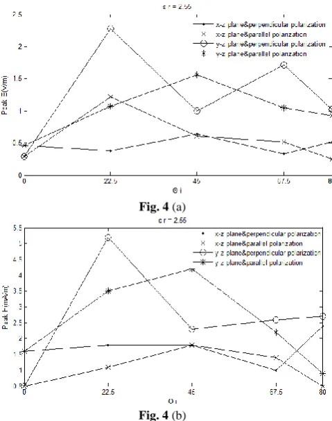
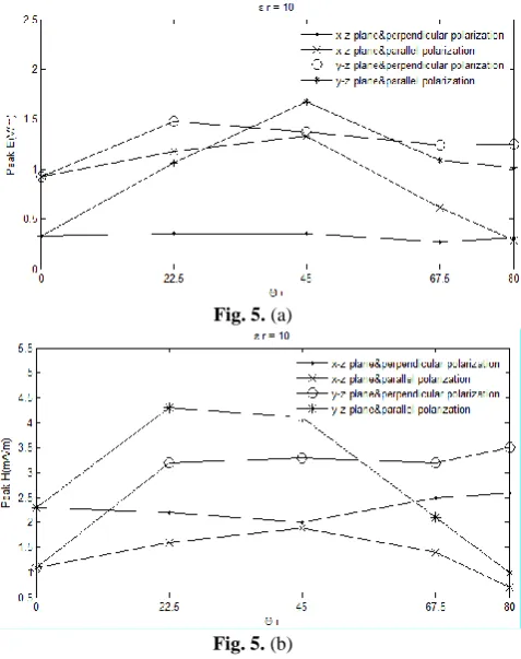
To examine the effect of external electromagnetic field to CPW line, two incidence planes consisted of x-z plane and y-z plane and, for each plane, two E-field polarizations (parallel and perpendicular polarizations relative to incidence plane) were considered. Simulations were performed for the incidence angles of 0, 22.5, 45, 67.5 and 80 degrees. Peaks of the induced electric and magnetic fields for the two CPW lines are shown in Figs. 4-5. It can be found for both CPW lines that the peaks of the induced electric and magnetic fields for the y-z incidence plane were larger than those for the x-z incidence plane for both parallel and perpendicular polarizations. Also, approximately for the incidence angles of 22.5˚ and 45˚,
maximum peaks of the induced field occurred. In addition, the simulated results showed the peaks of the induced electric and magnetic fields for the CPW line with εr = 2.55 were
approximately greater than those of the CPW line with εr = 10.
Figs. 6-7 show the induced electric field distribution of the center metal strip and cross-section of CPW lines with εr = 2.55
and εr = 10 for the incidence planes of x-z and y-z planes, θi =
22.5˚ and perpendicular polarizations. For the incidence planes of x-z and perpendicular polarizations that the incident electric field Ei directed as the y axis, it is observed that the induced
electric fields in the two slots of the CPW line were in the opposite direction and the even mode was propagated in the CPW line. For the incidence planes of y-z and perpendicular polarizations that the incident electricfield Ei directed as the x
axis, the induced electric fields in the two slots were in the same direction and the odd mode was propagated in the CPW line. Accordingly, the variation of the electric field distribution of along the CPW line was fasterin the CPW line with εr = 10
than the CPW line with εr = 2.25, which was due to higher
permittivity of the substrate.
Fig. 4 (a)
Fig. 4 (b)
Fig. 5. (a)
Fig. 5. (b)
Fig. 5. (a) Peaks of the induced electric field (b) Peaks of the induced magnetic field for the CPW line with εr = 10.
Fig. 6 (a)
Fig. 6 (b)
Fig. 6. Induced electric field distribution of the center metal strip and cross section of CPW lines with εr = 2.55 for θi = 22.5˚ ,
perpendicular polarizations and (a) incidence plane of x-z (b) incidence plane of y-z.
Fig. 7. (b)
Fig. 7. Induced electric field distribution of the center metal strip and cross section of CPW lines with εr = 10 for θi = 22.5˚ ,
perpendicular polarizations and (a) incidence plane of x-z (b) incidence plane of y-z.
Fig. 8. (a)
Fig. 8. (b)
Fig. 8. (a) Magnitude of the induced electric field (b) Magnitude of the induced magnetic field along the CPW lines with εr = 2.55
and εr = 10 for incidence angle θi = 0˚
Magnitude of the induced electric and magnetic fields along the CPW lines with εr = 2.55 and εr = 10 for incidence angle θi
= 0˚ (incident wave in the z direction) is shown in Fig. 8. For the CPW line with εr = 10, the magnitude of the induced
electric field when the incident electric field Ei directed as the
x axis was more than other states and the magnitude of the induced magnetic field when the incident electric field Ei
directed as the y axis was more than other states. In the case of incidence angle θi = 0˚, the amplitudes of the induced electric
and magnetic fields were approximately symmetric with respect to the center of the line. In this case as well, when the incident electric field Ei directed as the y axis, the even mode
was propagated and, when the incident electric field Ei directed
as the x axis, the odd mode was propagated.
IV.
C
ONCLUSIONSIn this paper, the coupling between an external electromagnetic field and the CPW line was investigated. The electric and magnetic fields induced along the line by the external plane wave were analyzed. Effects of the incidence plane, incidence angle and dielectric substrate permittivity on the coupling were evaluated. Two CPW lines with the characteristic impedance of 50Ω and dielectric substrate relative permittivity of 2.55 and 10 were considered. Both lines terminated with their characteristic impedance at both ends. For each case, two incidence planes and, for each plane, two E-field polarizations, parallel and perpendicular relative to incidence plane and incidence angles of 0, 22.5, 45, 67.5 and 80 degrees, were examined. The simulated results showed for the incidence angles of 22.5˚ and 45˚, maximum peaks of the induced field occurred. Also in these cases, depending on the incidence plane, incidence angle and E-field polarization, even or odd quasi-TEM mode of the CPW line could be propagated.
R
EFERENCES[1] D. Pissoort, M.Mechaik, H. Zeng, C. Shu, C. Jackson and J. V. Hese, “Performance degradation due to coupling between high-speed traces and on-board antennas,” IEEE International Symposiumon Electromagnetic Compatibility (EMC EUROPE ’13), pp. 282–287, IEEE, Brugge, Belgium, September 2013.
[2] J. Cho, E. Song, H. Kim, S. Ahn, J. S. Pak and J. Kim, “Mixed-mode ABCD parameters: Theory and application to signal integrity analysis of PCB-level differential interconnects,” IEEE Trans. Electromagn. Compat., Vol. 53, No. 3, pp. 814–822, Aug. 2011.
[3] I. Erdin and R. Achar, “Modeling of Asymmetric Differential Striplines Including Crossing Junction Discontinuities,” IEEE Trans. Electromagn. Compat., Vol. 60, No. 1, pp. 50–58, Feb. 2017.
Symposium on Electromagnetic Compatibility, 2008. [5] R. Zamir, V. Bar-Natan, and E. Recht, “System level EMC
from theory to practice,” International Symposium on Electromagnetic Compatibility, Vol. 3, 2005.
[6] T.-H. Lee, C.-G. Kim, J.-H. Lee, and J.-K. Wee, “Analysis of the EMI and SI effects on the flexible-PCBs for mobile application,” in Proceedings of the Electrical Design of Advanced Packaging and Systems Symposium(IEEE EDAPS ’08), pp. 97–100, December 2008.
[7] F. Rachidi, “A review of field-to-transmission line coupling models with special emphasis to lightning-induced voltages on overhead lines,” IEEE Trans. Electromagn. Compat., Vol. 54, No. 4, pp. 898–911, Aug. 2012.
[8] S. Sudekum, A. Mantzke, and M. Leone, “Efficient Modal Network Model for Nonuniform Transmission Lines Including Field Coupling,” IEEE Trans. Electromagn. Compat., Vol.58, No.4, pp. 1359-1366, Aug. 2016. [9] H. Xie, Y. Li, K. Yuan, and J. Wang, “Model for Fields
Coupling With Two Connected Transmission Lines With Different Reference Planes,” IEEE Trans. Electromagn. Compat., Vol.60, No.3, pp. 761-767, June. 2018.
[10] L. Yan, X. Zhang, X. Zhao, X. Zhou, and R.X-K. Gao, “A Fast and Efficient Analytical Modeling Approach for External Electromagnetic Field Coupling to Transmission Lines in a Metallic Enclosure,” IEEE Access, Vol. 6, pp. 50272-50277, 2018.
[11] Y. Yan, L. Meng, X. Liu, T. Jiang, and G. Zhang, “An FDTD Method for the Transient Terminal Response of Twisted-Wire Pairs Illuminated by an External Electromagnetic Field,” IEEE Trans. Electromagn. Compat., Vol.60, No.2, pp. 435-443, April. 2018.
[12] Z. Li, Z. Jiao, and M. Yuan, “Electromagnetic Coupling Analysis on Coaxial Cable of Aircraft Fuel Measurement System,” CSAA/IET International Conference on Aircraft Utility Systems (AUS 2018), 2018.
[13] D. M. Pozar, Microwave Engineering, 2nd ed. New York, NY, USA: Wiley, 1998.
[14] Paolo Bernardi, “Response of a planar microstrip line excited by an External electromagnetic field,” IEEE Transaction on Electromagnetic Compatibility. Vol. 32, No. 2, May 1990.
[15] H. Yan, L. Yan, X. Zhao, H. Zhou, and K. Huang, “Analysis of Electromagnetic Field Coupling to Microstrip Line Connected with Non-Linear Components,” Progress In Electromagnetics Research B, Vol. 51, pp. 291-306, 2013. [16] H. Lee, S. Ryu, S. Lee, S.Y. Kim, and W. Nah,
“Electromagnetic Field Interference on Transmission Lines due to On-Board Antenna,” Hindawi Publishing Corporation, International Journal of Antennas and Propagation, Vol. 2015, pp. 1-12, 2015.
[17] H. R. Goodarzi, M. Tayarani and S. Khosravi, “Differential to common mode coupling in microstrip lines; calculation and Improvement,” 18th Int. Zurich Symposium on EMC, Munich 2007.
[18] M. Hashemi-Nasab and A. Cheldavi, "Coupling Model for the Two Orthogonal Microstrip Lines in Two Layer PCB Board (Quasi-TEM Approach)", Progress In ElectromagneticsResearch, PIER 60, pp. 153-163, 2006. [19] A. Cheldavi and A. Arshadi, "A Simple Model for the
Orthogonal Coupled Strip Lines in Multilayer PCB: (Quasi-TEM Approach)", Progress In Electromagnetics Research, PIER 59, pp. 39-50, 2006.
[20] R. N. Simons, Coplanar Waveguide Circuits, Components,
and Systems. John Wiley & Sons, Inc.2001.
[21] High Frequency Software Simulator (HFSS). ver. 13, Ansoft Corporation.