Semiconductor Nanowires
Photovoltaic Devices
Coatings
Biosensors
Drug Delivery
Fuel Cells
Structural Nanocomposites
Nanomaterials Y
ester
day
,
Today and T
omorr
ow
TO ORDER: Contact your local Sigma-Aldrich office (see back cover), call 1-800-325-3010 (USA), or visit sigma-aldrich.com.
sigma-aldrich.com
Nanomaterials Yesterday, Today and Tomorrow
Mr. Thomas Juehne, Sigma-Aldrich Corp., St. Louis, MO
The union of distinct scientific disciplines is revealing the leading edge of Nanotechnology. Fifteen to twenty years ago, the interdisciplinary activity of geneticists, biologists, immunologists and organic chemists created a more diverse toolbox now known as life science. Bioconjugates were created to help us move from outside the cell to the inside. Enabling technologies brought about the ability to
create, identify and specifically manipulate genetic maps to engineer designer proteins.1 In parallel,
physicists, chemists, polymer chemists and engineers were creating the foundation for the small world
of nano materials science. Fullerenes,2 carbon nanotubes3 and atomic force microscopy4were in their
infancy. In less than a decade, materials science and life science together are unraveling the mysteries of controlling, on a molecular level, the structure of matter.
Particles, complexes, tubes, coatings, active surfaces and devices are being explored on the nanoscale. Assembly of nature’s building blocks (e.g. carbon, nucleic acids, lipids and peptides) along with the combination of different materials (e.g. CdSe/ZnS, Au, Ag, Si(n)OH(n), light harvesting dendrimers and thin films) are leading to insightful understanding and the creation of new scientific tools. Chemists and physicists have been manipulating matter on the molecular level for centuries. Some say this is nothing new. When one looks at the absolute elegance of the nanometer scale biological system, how-ever, one is compelled to create, understand, manipulate and control systems with equal elegance.
This high level of activity and promise has attracted private and government funding with consider-able economic impact and growth. Since the launch of the National Nanotechnology Initiative
(www.nano.gov)in 2000, there have been hundreds of start-up companies emerging in the market. At universities, there are increased investments in nanotechnology programs and facilities. Northwestern
University’s Institute for Nanotechnology (www.nanotechnology.northwestern.edu)is a direct result of
the high level of activity and pioneering work of Prof. Chad Mirkin. As a result of massive grant sup-port and continued focus from the university, the Center for Nanofabrication and Molecular Self
Assembly building has been constructed. Similarly, The Molecular Foundry (www.foundry.lbl.gov), a
Department of Energy Nanoscale Science Research Center, is under construction at Berkeley in California. The research center is focused on the dissemination of nanoscale techniques and methods to enable scientists to delve into nano research. The Molecular Foundry is the direct result of Prof. Paul Alivasatos’ discoveries and benchmark work. We see an increase in programs, facilities, career oppor-tunities and educational outreach. It is a massive explosion of activity in study on a very small scale. Science is beginning to set free nanotechnology. Soon the only limit will be the imagination.
Acknowledgements
Sigma-Aldrich would like to grate-fully acknowledge the contribu-tors to this applications guide, especially Prof. William E. Buhro, Dr. Sean Dingman, Mr. Thomas Juehne, Prof. Nicholas A. Kotov, Prof. Yuri Lvov, Prof. Shelley D. Minteer, Prof. Pradeep K. Rohatgi and Prof. Michael Strano.
About the Cover
The cover image depicts part of a MEMS actuator (image courtesy of MEMSX, http://www.memx.com/products.htm) in the foreground as well as a molecular model of a single-walled carbon nanotube (image courtesy of Prof. Chris Ewels). The background image shows a tight-knit mesh of nanofibrils with a human hair overlaid for a size comparison (image courtesy of Espin Technologies, Inc.).
“Please Bother Us.”
Sigma-Aldrich invites your feedback on this brochure. We would be happy to assist you with
Nanoparticle-Catalyzed Growth of Semiconductor Nanowires
Prof. William E. Buhro, Deptartment of Chemistry, Washington University, St. Louis, MO
Answers from the Past
Over the past twenty years, homogeneous nucleation in solution has proven to be an effective method for
the synthesis of both metallic5 and semiconductor nanocrystals.6 Nearly isotropic, pseudospherical
mor-phologies are typically produced. Other nanocrystalline mormor-phologies are often desirable, and
homoge-neous nucleation has been adapted for the synthesis of rod-shaped morphologies.7 However, the growth
of nanowiresby homogeneous nucleation is apparently limited to materials having particularly favorable,
highly anisotropic crystal structures.8 How then might nanowire morphologies be generally prepared?
The answer was uncovered by Wagner and Ellis in 1964,9 who discovered that micrometer-scale silicon
whiskers (wires) could be grown from gold-droplet catalysts under Chemical Vapor Deposition (CVD) con-ditions at about 1000 °C. The process was named the “Vapor-Liquid-Solid” (VLS) mechanism after the three phases involved. VLS growth was extended to micrometer-scale whiskers of many inorganic materials and intensively studied for over a decade, before fading into relative obscurity.
From VLS to SLS
In 1995, my group reported that III-V semiconductor nanowires could be grown in solution from indium nanoparticle catalysts by a process analogous to the VLS mechanism, and by analogy we named it the
“Solution-Liquid-Solid” (SLS) mechanism.10 Shortly thereafter,
Lieber and coworkers described laser-ablation adapta-tions of the VLS mechanism that afforded silicon and a wide range of other semiconductor nanowires
(Laser-Assisted Catalyzed Growth, LCG).11-12 Many others made
seminal contributions to nanowire growth by VLS adap-tations, most notably Korgel (Supercritical
Fluid-Liquid-Solid, SFLS, mechanism)13and Yang.14 We now routinely
prepare soluble, III-V and II-VI semiconductor nanowires with controlled diameters in the strong-confinement regime of about 3–20 nm by
bismuth-nanoparticle-cat-alyzed SLS growth (Figure 1).15-16 The
nanoparticle-cat-alyzed VLS mechanism and its solution-phase variants
have emerged as thepopular, widely practiced, general
methods for the synthesis of semiconductor nanowires.17
Gold nanoparticles are presently by far the most com-monly employed catalysts.
Quantum Wires to Nanophotonics
The advantages of nanoparticle-catalyzed nanowire growth include its general applicability to a wide vari-ety of materials, the diameter control afforded, the uniformity of the wires (lack of significant diameter fluctuations) and their oriented, near-single crystallinity. The surface passivation, solubility and length of the wires may also be systematically varied. Small-diameter “quantum” wires are ideal specimens for fun-damental studies of two-dimensional (2D) quantum-confinement phenomena and for property compar-isons to 3D-confined quantum dots, 1D-confined quantum wells and anisotropically 3D-confined quantum rods. Potential applications of semiconductor nanowires in nanophotonics and lasing, nanoelectronics, solar-energy conversion and chemical detection are under active development. Exciting progress and advances in the semiconductor-nanowire field, enabled by the emergence of nanoparticle-catalyzed growth, are anticipated in the immediate future.
For gold nanoparticles, see page 7.
Nanoparticle-Catalyzed
Gr
owth of Semiconductor
Nanowir
es
Order: 1.800.325.3010 T
echnical Service: 1.800.231.8327
Nanomaterials in Organic
Photovoltaic Devices
TO ORDER:
Contact your local Sigma-Aldrich office (see back cover), call 1-800-325-3010 (USA), or visit sigma-aldrich.com.
sigma-aldrich.com
Nanomaterials in Organic Photovoltaic Devices
Dr. Sean Dingman, Sigma-Aldrich Corp., Milwaukee, WI
The ability to create high-efficiency solar cells is a key strategy to meeting growing world energy needs. Nanotechnology is currently enabling the production of high-efficiency organic photovoltaics (OPVs) to
help meet this challenge.18Organic photovoltaics are nanostructured thin films composed of layers of
semi-conducting organic materials (polymers or oligomers)19that absorb photons from the solar spectrum. These
devices will revolutionize solar energy harvesting, because they can be manufactured via solution-based methods, such as ink-jet or screen printing, enabling rapid mass-production and driving down cost.
OPVs currently lag behind their “inorganic” counterparts because of low solar energy conversion efficien-cies (approximately 1-3%). Several research groups are addressing conversion efficiency by employing a combination of nanomaterials and unique nanoscale architectures. These hybrid organic-inorganic photo-voltaics consist of light-absorbing polymers in contact with semiconductor nanocrystals, fullerenes or nanos-tructured metals. The nanomaterials affect electro-optical properties of the conducting polymer, which include assisting in absorption of red and near-IR photons, a significant portion of the solar spectrum.
Examples of OPVs designs employing nanomaterials include:20-23
Polymer-Fullerene Heterojunctions: Cells where a chemically modified fullerene (C60) layer, acting as
electron acceptors, is in close physical contact with a polymeric organic electron donor (MDMO-PPV
catalog number 546461, or poly-(3-hexylthiophene), P3HT, catalog number 445703and 510823). This
contact improves efficiency by allowing charge transfer to take place at the sub 10-nanometer scale, on the order of the diffusion length of an exciton generated from organic semiconductors. The most recent cells exhibit conversion efficiencies of ~5%.
Organic-Nanocrytsal Solar Cells:Blends of semiconducting polymers and semiconducting quantum dots or nanorods (CdSe or CdTe) are mixed in a manner similar to the polymer-fullerene blends. The poly-mers are modified to give rise to chemical bonding between the nanocrystal and polymer. The nanocrystals can be tailored to a wide variety of optical band gaps, which depend on the size of the nanocrystal (or the diameter of the nanorod).
Dye-Sensitized Cells: These cells employ complex dye molecules attached to the surface of
nanostruc-tured oxides like titanium(IV) oxide (TiO2) or niobium(V) oxide (Nb2O5). The dyes exhibit broad
light-absorption profiles and rapid photoinduced charge transfer of electrons to the nanocrystals. These cells show solar conversion efficiencies of ~4%.
Tandem Cells: The tandem cell acts as a 2-1 cell, harvesting photons from the complete visible spectrum. These cells
employ layers of C60as a strong blue light absorber and
copper-phthalocyanine (CuPc) as a red-yellow absorber. Nanosized silver particles act as a charge conduit between the cells but do not absorb photons traveling through the cell because of their nanosized dimensions. These cells have achieved conversion efficiencies of
~6% (Figure 2).
Significant challenges exist to achieving OPV devices that can be mass-produced. Nanotechnology will assist in meeting the technical challenges of this rapidly evolving field.
Avg. Particle
Catalog # Composition Size (nm) Purity (%)
484059 Silver 100 99
576832 Silver 70 99.5
Figure 2. Schematic of tandem organic photovoltaic cells.24
Organic Semiconductors for Advanced Electronics
Request your free copy today. Contact the product manager,
Coatings
Dr. Luke Grocholl, Sigma-Aldrich Corp., Milwaukee, WI
Nanopowders and nanoparticle dispersions have seen increasing applications in coatings. Due to their small size, very even coating can be achieved by painting nanoparticle dispersions onto a surface and baking off the residual solvent.
Optically Transparent Conductive Coatings:Indium tin oxide (ITO) and antimony tin oxide (ATO) are well known, optically transparent, electrically conductive materials. Nanoparticles of these materials can be painted on surfaces such as interactive touch screens to cre-ate a conductive, transparent screen
without relying on expensive sputter-ing techniques. In addition, ITO and ATO can be used as an antistatic coat-ing, utilizing their inherent conduc-tivity to dissipate static charge.
Optically Transparent Abrasion-Resistant Coatings: Nanoscale alu-minum oxide and titanium oxide are optically transparent and greatly increase the abrasion resistance of traditional coatings. Titanium oxide is of particular interest in many opti-cal applications, since it is highly reflective for most ultra-violet radia-tion. Zinc oxide and rare-earth oxides are also UV-reflective, but optically transparent and are there-fore effective in protecting surfaces from degradation brought about by exposure to UV radiation.
Coatings
Order: 1.800.325.3010 T
echnical Service: 1.800.231.8327
Avg. Particle
Catalog # Composition Formula Size (nm) Purity (%)
637262 Titanium(IV) oxide (rutile) TiO2 10 X 40* 99.5
637254 Titanium(IV) oxide (anatase) TiO2 5-10 99.7
634662 Titanium(IV) oxide (anatase) TiO2 60-100 99.9
544906 Zinc oxide ZnO 50-70 97.5
637289 Dysprosium(III) oxide Dy2O3 60-100 99.9+
637343 Erbium(III) oxide Er2O3 40-60 99.9+
634298 Europium(III) oxide Eu2O3 60-100 99.5+
637335 Gadolinium(III) oxide Gd2O3 40-60 99.9+
637327 Holmium(III) oxide Ho2O3 40-60 99.9+
634611 Neodymium(III) oxide Nd2O3 <40 99.9+
634263 Praseodymium(III,IV) oxide Pr6O11 <125 99
637319 Samarium(III) oxide Sm2O3 10-80 99.9+
634255 Terbium(III,IV) oxide Tb4O7 60-100 99.5
637300 Ytterbium(III) oxide Yb2O3 40-60 99.7+
544892 Yttrium(III) oxide Y2O3 25-30 99
* Average dimensions of crystallites
Avg. Particle Catalog # Composition Size (nm)
549541 Antimony tin oxide 19
544876 Indium tin oxide 25-45
Sigma-Aldrich offers several grades of fullerenes for your materials applications.
Catalog # Fullerene Type Purity (%)
572497 Fullerene soot, as produced (ca. 76% C60, 22% C70) 7
483036 Fullerene-C60 98
379646 Fullerene-C60 99.5
572500 Fullerene-C60 99.9
377120 Fullerite (ca. 90% C60, 10% C70) —
Catalog # Fullerene Type Purity (%)
379654 (5,6)-Fullerene-C70 95
482994 (5,6)-Fullerene-C70 99
482951 Fullerene-C76 98
482978 Fullerene-C78 98
482986 Fullerene-C84 98
Catalog # Fullerene Type Structure Purity (%)
64251 (1,2-Methano- 97+
fullerene C60 )-61-carboxylic acid
64246 Ethyl (1,2-methano- 95+
fullerene C60 )-61-carboxylate
64245 tert-Butyl (1,2-methano- 95+
fullerene C60 )-61-carboxylate
Catalog # Fullerene Type Structure Purity (%)
64247 Diethyl (1,2-methano- 95+
fullerene C60)-61,61 -dicarboxylate
64248 Diethyl (1,2-methano- 95+
fullerene C70 )-71,71-dicarboxylate
OH O
O O
O O
O O
O O
O O
Carbon Nanotube- Based Biosensors
sigma-aldrich.com
Carbon Nanotube-Based Biosensors
Prof. Michael Strano, Dr. Seunghyun Baik, Paul Barone, Department of Chemical and Biological Engineering, University of Illinois at Urbana-Champaign, Urbana, IL
Bio-conjugates
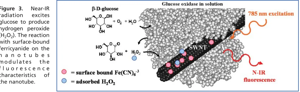
Researchers from the University of Illinois at Urbana-Champaign have developed near-infrared optical biosensors based on single-walled carbon nanotubes, which modulate their fluorescence emission in response to specific biomolecules. The viability of sensor techniques was demonstrated by creating a
single-walled carbon nanotube (SWNT) enzyme bio-conjugate that detects glucose concentrations.25
Carbon nanotubes fluoresce in a region of the near-infrared, where human tissue and biological fluids are particularly transparent to their emission. The sensor could be implanted into tissue, excited with a near-infrared light source, and provide real-time, continuous sensing of blood glucose level by fluorescence
response. Figure 3shows a schematic mechanism of the nanotube sensor. Hydrogen peroxide is produced
when glucose reacts with the enzyme, which quickly transforms ferricyanide to modulate near-infrared flu-orescence characteristics of the nanotube.
Future Opportunities
The important aspect of this technology is that the technique can be extended to many other chemical sys-tems. New types of non-covalent functionalization are developed, creating opportunities for nanoparticle sensors that operate in strong absorbing media of relevance to medicine or biology.
Figure 3. Near-IR radiation excites glucose to produce hydrogen peroxide (H2O2). The reaction with surface-bound ferricyanide on the n a n o t u b e s m o d u l a t e s t h e f l u o r e s c e n c e characteristics of the nanotube.
Figure 4. A size compar-ison of a SWNT-based g l u c o s e detector on a fingertip.
Synthetic Diameter Length
Catalog # Nanotube Type Method (nm) (nm) Purity (%)
519308 Single-walled, CarboLexTM AP-grade Arc 1.2-1.5 2-5 50-70
589705 Single-walled, as produced Arc 0.9-1.2 10-30 12-15
652512 Single-walled, short CVD 0.8-1.6 ~0.5 90+
636797 Single-walled CVD 0.8-1.6 0.5-100 90+
Layer
-by-Layer Nanoassembly
for Drug Delivery and
Antibacterial Applications
Order: 1.800.325.3010 T
echnical Service: 1.800.231.8327
Layer-by-Layer Nanoassembly for Drug Delivery
Prof. Yuri Lvov, Institute for Micromanufacturing, Louisiana Tech University, Ruston, LA
Researchers from Louisiana Tech University were among the pioneers of one of the novel nanotechnology methods: layer-by-layer (LbL) nanoassembly by alternate adsorption of oppositely charged polyelectrolytes, nanoparticles and proteins. With this technique, we can assemble ultrathin multilayers with nanometer precision and pre-determined composition across the film, and make nanocapsules from LbL films. We are using such nanocapsules for targeted drug delivery, biocompatible nanocoating and pulp microfiber pro-cessing. For this nanoarchitecture, we use nanoblocks, such as nanoparticles. In the development of our research area, we successfully used nanoparticles, such as different diameter and surface-charged gold nanoparticles, silica, nanoclay-montmorillonite, alumina, titanium dioxide and other nanoparticles. Also, we investigated linear polyelectrolytes of different types and molecular weight (especially natural poly-electrolytes), which we used as electrostatic glue to assemble nanoparticle and protein arrays. As any archi-tect, we nanoarchitects need a wide palette of nanoblocks with new properties and dimensions, ideally, monodispersed, stable in solution, charged nanoparticles of noble metals, metal oxides and ceramics with diameters of 5, 10, 20, 50 and 100 nm.
Wt% Avg. Specific
Dispersion Particle Purity Conductivity Surface Area Catalog # Composition (in Water) Formula Size (nm) (%) pH (mS/cm) (m2/g)
643092 Aluminum oxide 5 Al2O3 <20 99.9 4-5 100-400 >100
642991 Aluminum oxide 10 Al2O3 <20 99.9 4-5 100-500 >100
643130 Silicon dioxide, alumina doped 5 SiO2 <20 99.99+ 5-7 <20 150-175
643084 Silicon dioxide, alumina doped 10 SiO2 <20 99.99+ 5-7 30-40 150-175
643114 Titanium(IV) oxide 5 TiO2 <40 99.9+ 2-3 400-800 20-40
643017 Titanium(IV) oxide 10 TiO2 <40 99.9+ 2-3 600-1000 20-40
Avg. Particle Catalog # Material Size (nm)
636347 Gold nanopowder, 99.9% 50-130
G 1402 Gold nanoparticle, aqueous suspension* 3.5-6.5
G 1527 Gold nanoparticle, aqueous suspension* 8-12
G 1652 Gold nanoparticle, aqueous suspension* 17-23
*Contains ~0.02 % NaN3as a preservative, <0.01% sodium citrate as a stabilizer, ~0.01 % HAuCl4and <0.01% tannic acid
Sigma-Aldrich offers gold nanoparticles and gold colloids as well as other aqueous nanoparticle suspensions.
Antibacterial Applications
Dr. Luke Grocholl, Sigma-Aldrich Corp., Milwaukee, WI
Zinc oxide is an effective antibacterial and anti-odor agent. It has been used in deodorants, dental cleansers and diaper creams. The increased ease in dispersibility, optical transparence and smoothness make zinc oxide nanopowder an attractive antibacterial ingredient in many heath care products. Copper oxide nanopowder has also been proposed as an anti-microbial preservative for wood or food products.
Avg. Particle
Catalog # Composition Formula Size (nm) Purity (%)
544868 Copper(II) oxide CuO 30-40 98
sigma-aldrich.com
Nanomaterials in Fuel Cells & Nanomaterials in Other
Energy Applications
Nanomaterials in Fuel Cells
Prof. Shelley D. Minteer, Department of Chemistry, Saint Louis University, St. Louis, MO
Over the last two decades, general interest and research in fuel cells has increased, because they have the
potential to be more energy efficient than conventional power generation methods.26 During this time
period, researchers have begun using nanomaterials in the catalyst layer of fuel cell electrodes for a variety of reasons, including: increasing the active surface area of the anode and cathode catalyst, increasing the catalytic rate of oxidation or reduction and minimizing the weight of platinum and other precious metals in the fuel cell. The current generated at an electrode is proportional to the active surface of catalyst on the electrode surface, so higher power density fuel cells can be formed from nanomaterials, because nano-materials have a higher surface area to volume ratio. Researchers have also shown that the electrocatalyt-ic properties of the materials are sensitive to partelectrocatalyt-icle size, so increased catalytelectrocatalyt-ic activity can be observed for
nanoparticles and nanomaterials.27-29 However, the most important goal has been to decrease the weight
of platinum and other precious metals in the catalyst layer of the fuel cell, so that the fuel cell can be
cost-effective. This has been the main limitation to the widespread use of fuel cells.26 Researchers have employed
carbon nanomaterials as supports for dispersions of platinum nanomaterials. This allows for a decrease in the weight of platinum needed to produce the same surface area of active platinum catalyst. The
nano-materials could be carbon foams containing nanopores,30 different types of nanotubes31-32or even
single-walled nanohorns.33 All of these materials can act as a support and a conductor for platinum
nanomateri-als, making strides toward cost-effective fuel cell catalysts.
For single-walled carbon nanotubes see page 6, for multi-walled carbon nanotubes see page 11.
Nanomaterials in Other Energy Applications
Dr. Luke Grocholl, Sigma-Aldrich Corp. Milwaukee, WI
Environmentally Friendly Energy Sources
Devising schemes to meet the world’s growing energy demands while simultaneously reducing green house emis-sions and other pollutants, has become one of the major challenges facing materials scientists. Nanomaterials promise to help solve many of the problems associated with new and emerging energy technologies.
Fuel Cells: Solid oxide fuel cells (SOFCs) offer the advantage over other fuel cell designs in that they do not require expensive, precious metal catalysts and can operate effectively without extensive purification of fuel sources. The activity of doped rare-earth oxide electrodes such as yttrium stabilized zirconia (YSZ) is directly relat-ed to their surface areas. Nanoparticles exhibit the high surface requirrelat-ed for developing SOFC technologies.
Cleaner Emissions:Catalytic converters on vehicles around the world have significantly reduced the amount of automotive pollution over the last three decades. These devices require large amounts of expensive metals such as platinum, palladium and rhodium. Doped rare-earth metal oxides offer the promise of increased catalytic activity without the heavy reliance on precious metals. In addition, the increased efficiency of the next-genera-tion catalytic converters will result in cleaner emission of existing internal combusnext-genera-tion and diesel engines.
Dopant/ Wt. % Avg. Particle Specific Surface Catalog # Composition Stabilizer Stabilizer Size (nm) Area (m2/g)
544760 Zirconium(IV) oxide 20-30 30-40
544779 Zirconium(IV) oxide Yttria 10 20-30 30-40
572349 Zirconium(IV) oxide Yttria 8 100 100-120
572322 Zirconium(IV) oxide Yttria 3 100 100-120
572357 Cerium(IV) oxide Gadolinium 20 100 100-120
572365 Cerium(IV) oxide Samaria 15 100 100-120
572381 Cerium(IV) oxide Yttria 15 100 100-120
572403 Cerium(IV) oxide Calcium 10 100 100-120
572330 Cerium(IV) oxide Gadolinium 10 100 100-120
Nanotube-Polymer Composites
for Ultra Str
ong Materials
Order: 1.800.325.3010 T
echnical Service: 1.800.231.8327
Nanotube-Polymer Composites for Ultra Strong Materials
Prof. Nicholas A. Kotov, Department of Chemical Engineering, University of Michigan, Ann Arbor, MI
Exceptional Strength
Exceptional mechanical properties of single-walled carbon nanotubes (SWNT) have prompted intensive studies of SWNT-polymer composites. However, the composites made with nanotubes are still holding a substantial reserve of improvement of mechanical properties. The problem is that pristine SWNTs have very poor solubility in polymers, which leads to phase segregation of composites. Severe structural inhomo-geneities result in the premature failure of the hybrid SWNT-polymer materials. The connectivity with the polymer matrix and uniform distribution within the matrix are essential structural requirements for strong SWNT composites. This problem is being solved by several approaches. First, by using coatings from sur-factants and polymers, such as sodium dodecyl sulfate or poly(styrenesulfonate). This enables formation of better dispersions in traditional solvents including water. Polymeric dispersion agents are strongly pre-ferred for the composite preparation because of (a) tighter bonding with the graphene surface, (b) misci-bility with polymer matrixes of composites and (c) substantially smaller concentration necessary for the preparation of SWNT dispersions. Among polymers, different poly(vinyl alcohols) work best as a host matrix for SWNTs, providing the composites with high tensile strength and excellent Young’s modulus.
Looking Ahead
An additional resource of SWNTs for improving the mechanical properties of composites is nanotube ori-entation. Virtually complete alignment of nanotubes can be achieved in SWNT composite fibers. These composites display substantially better mechanical properties than any other SWNT-polymer hybrid. If one can find a simple and controllable method to produce not only fibers but also bulk materials and coatings with nanotubes oriented in a desirable direction, new technological vistas can be opened for various com-posites. Breakthroughs in this area can come both from the studies of fundamental properties of SWNTs and from development of methods for composite processing. In the past, magnetic field alignment with exceptionally powerful electromagnets and alignment in the flow was used for this purpose.
Diameter Length CNT Loading Solubility Catalog # Nanotube Type Structure (nm) (mm) Purity (%) (%) (mg/mL)
652490 Single-walled, 4-5 0.5-1.5 80-90 3-6 H2O 0.1
carboxylic acid DMF 1.0
functionalized (3-6 atomic %)
639230 Single-walled, 1.1 0.5-100 70-85 65 H2O 5.0
PABS (polyamino DMF 0.1
benzoic acid) EtOH 0.05
coated (65 wt.%)
652474 Single-walled, 4-5 0.5-0.6 80-90 30 H2O 5.0
PEG (polyethylene glycol) coated (30 wt. %)
652482 Single-walled, 2-8 0.5-1.0 80-90 30-40 THF >1.0
ODA CS2>1.0
(octadecylamine) benzene >1.0
coated toluene >1.0
(30-40 wt. %) 1,2-dichlorobenzene >1.0
OH O
H N O
SO3H
H N
n
O O
n
O
HN CH2
17
CH3
Metal Matrix
Nanocomposites for
Structural Applications
sigma-aldrich.com
Metal Matrix Nanocomposites for Structural Applications
Prof. Pradeep K. Rohatgi; Ben Schultz; J.B. Ferguson, University of Wisconsin-Milwaukee Center for Composites, Milwaukee, WI
Improved Properties
Metal matrix composites (MMCs) such as continuous carbon or boron fiber reinforced aluminum and mag-nesium, and silicon carbide reinforced aluminum have been used for aerospace applications due to their
lightweight and tailorable properties.34There is much interest in producing metal matrix nanocomposites
that incorporate nanoparticles and nanotubes for structural applications, as these materials exhibit even greater improvements in their physical, mechanical and tribological properties as compared to composites
with micron-sized reinforcements.35-39 The incorporation of carbon nanotubes in particular, which have
much higher strength, stiffness, and electrical conductivity as compared to metals, can significantly increase these properties of metal matrix composites. Nanocomposites are being explored for structural applications in the defense, aerospace and automotive sectors.
Low Cost Solutions
Concurrent with the interest in producing novel nanocomposite materials is the need to develop low cost means to produce these materials. Most of the prior work in synthesizing nanocomposites involves the use of powder metallurgy techniques, which are not only high cost, but also result in the presence of porosity
and contamination.26, 40-41 Solidification processing methods, such as stir mixing, squeeze casting and
pres-sure infiltration are advantageous over other processes in rapidly and inexpensively producing large and complex near-net shape components, however, this area remains relatively unexplored in the synthesis of
nanocomposites. Stir mixing techniques, widely utilized to mix micron size particles in metallic melts,42-43
have recently been modified for dispersing small volume percentages of nanosize reinforcement particles in metallic matrices. Although there are some difficulties in mixing nanosize particles in metallic melts resulting from their tendency to agglomerate, a research team in Japan has published research on
dispers-ing nanosize particles in aluminum alloys usdispers-ing a stir mixdispers-ing technique.44 Researchers at the Polish Academy
of Science45have recently demonstrated the incorporation of greater than 80 volume percent nanoparticles
in metals using high-pressure infiltration with pressures in the GPa range. Composites produced by this method possess the unique properties of nanosize metallic grains.
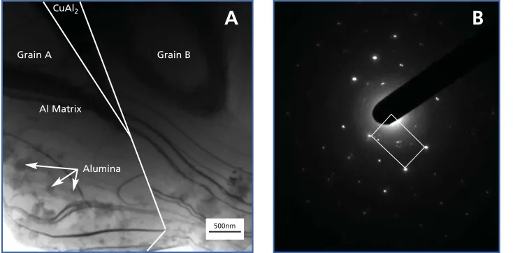
Recently, metal matrix nanocomposites were synthesized at the University of Wisconsin, Milwaukee using
aluminum alloy A206 and nanoparticles of alumina (Al2O3).46 TEM samples of the cast Al-A206/Al2O3
clear-ly show nanoparticles present within the metal matrix (Figure 5A). SAD patterns show the pattern of the
matrix as well as the nanoparticles (Figure 5B). EDX indicates that the grains are composed of aluminum,
which contains nanosize alumina particles. The distribution of particles throughout the grains of the matrix with an absence of large concentrations at the grain boundaries suggests wetting of the alumina by the liq-uid metal. In this case the nanoparticles did not appear to act as nucleation sites for nanosized grains.
Figure 5A. Nanosize Al2O3
particles embedded in cast aluminum matrix.
Figure 5B. Diffraction Pattern; the nanocomposite was synthe-sized at the University of Wisconsin, Milwaukee (TEM by Dr. M. Gajdardziska-Josifovska, Co-PI).
A
B
CuAl2
Grain A Grain B
Al Matrix
Alumina
Books on Nanomaterials
and Nanotechnology
Order: 1.800.325.3010 T
echnical Service: 1.800.231.8327
Sigma-Aldrich offers several structural nanopowders as well as a variety of multi-walled nanotubes.
Avg. Particle
Catalog # Composition Formula Size (nm) Purity (%)
544833 Aluminum oxide Al2O3 40-50 98
551643 Aluminum oxide, whiskers Al2O3 2-4 X 2800 99
594911 Silicon carbide (primarily beta-phase) SiC 45-55 97.5
636967 Titanium carbide TiC 130 98+
636940 Titanium carbonitride (C 7:N 3) TiC0.7N0.3 <80 97+
636959 Titanium carbonitride TiC0.5N0.5 <80 97+
Outer Inner
Synthetic Diameter Diameter Length
Catalog # Nanotube Type Method (nm) (nm) (nm) Purity (%)
637351 Double-walled CVD <5 1.3-2.0 0.5-50 50-80†
636819 Multi-walled, purified CVD <8 2-5 0.5-200 95+
412988 Multi-walled, as produced Arc 6-20 * 1-5 8-10
406074 Multi-walled, powdered cylinder cores Arc 6-20 * 1-5 30-40
636541 Multi-walled, purified CVD 3-20 1-3 0.1-10 90+
636525 Multi-walled, purified CVD 10-20 5-10 0.5-200 95+
636517 Multi-walled, purified CVD 10-30 3-10 1-10 90+
636509 Multi-walled, purified CVD 10-30 5-10 0.5-50 95+
636495 Multi-walled, purified CVD 20-30 1-2†† 0.5-2 95+
636487 Multi-walled, purified CVD 20-30 5-10 0.5-200 95+
636614 Multi-walled, purified CVD 20-40 5-10 0.5-50 95+
636649 Multi-walled, purified CVD 20-50 1-2†† 0.5-2 95+
636630 Multi-walled, purified CVD 30-50 5-15 0.5-200 95+
636622 Multi-walled, purified CVD 40-60 5-10 0.5-500 95+
636843 Multi-walled, purified CVD 40-70 5-40 0.5-2 95+
636835 Multi-walled, purified CVD 60-100 5-10 0.5-500 95+
636398 Graphite, nanofibers CVD 80-200 0.5-10 0.5-20 95+
Books on Nanomaterials and Nanotechnology
The Chemistry of Nanomaterials: Synthesis, Properties and Applications, 2 volumes (Catalog #Z703850)
C. N. R. Rao, A. Müller, A. K. Cheetham (Eds.), Wiley, 2004
With this handbook, the distinguished team of editors has combined the expertise of leading nanomaterials scientists to provide the latest overview of this field. The authors cover the whole spectrum of nanomaterials, ranging from theory, synthesis, properties, characterization and applications.
Nanoparticles: From Theory to Applications (Catalog # Z551376)
G. Schmid (Ed.), Wiley, 2004
An introduction to the science of nanoparticles, from fundamental principles to their use in novel applications. As a basis for under-standing nanoparticle behavior, the book first outlines the principles of quantum size behavior, nanoparticles architecture, forma-tion of semiconductor and metal nanoparticles. It then goes on to describe the chemical syntheses of nanoparticles with defined char-acteristics, their structural, electrical and magnetic properties, as well as current methods to monitor these properties.
References
1) Regan L.; DeGrado W.F. Science1988, 241, 976. 2) Kroto H.W. et al. Nature1985, 318, 162. 3) Iijima, S. Nature1991, 354, 56. 4) Binnig, G.; Rohrer, H. Rev. of Mod. Phys., 1987, 59, 615. 5) Watzky, M.A.; Finke, R.G. J. Am. Chem. Soc.1997, 119, 10382. 6) Murray, C.B. et al. J. Am. Chem. Soc.1993, 115, 8706. 7) Peng, X. et al. Nature2000, 404, 59. 8) Gates, B. et al. Adv. Funct. Mater.2002, 12, 219. 9) Wagner, R.S.; Ellis, W.C. Appl. Phys. Lett.1964, 4, 89. 10) Trentler, T.J. et al. Science1995, 270, 1791. 11) Morales, A.M.; Lieber, C.M. Science1998, 279, 208. 12) Duan, X.; Leiber, C.M. Adv. Mater. 2000, 12, 298. 13) Holmes, J.D. et al. Science2000, 287, 1471. 14) Wu, Y.; Yang, P. J. Am. Chem. Soc.2001, 123, 3165. 15) Yu, H. et al. Nature Mater.2003, 2, 517. 16) Yu, H. et al. J. Am. Chem. Soc.2003, 125, 16168. 17) Xia, Y. et al. Adv. Mater. 2003, 15, 353. 18) Smalley, R.E. “Nanotechnology, Energy and People” http://www.americanenergyindependence.com/energychallenge.html, accessed Feb 23, 2005. 19) To review a complete list of semiconducting polymers and oligomers, request your free copy of ChemFiles Vol. 4 No. 6: Organic Semiconductors for Advanced Electronics. 20) McGhee, M.D.; Coakley, K.M. Chem. Mater.2004, 16, 4533. 21) Shaheen, S.E. et al. Mater. Res. Bull.2005, 30, 10. 22) Hoppe, H.; Sariciftci, N.S. J. Mater. Res, 2004, 19, 1924. 23) Nierengarten, J.-F. New. J. Chem.2004, 28, 1177. 24) Xue, J. et al. Appl. Phys. Lett.2005, 86, 5757. 25) Strano, M.S. et al. Nat. Mater.2005, 4, 86. 26) Kordesch, K.; Simader. G. Fuel Cells and Their Application(VCH, Weinheim, 1996). 27) Brayner, R. et al.J. Mol. Catal. A: Chem.2002, 182, 227. 28) Liu, C. et al. J. Mol. Catal. A: Chem. 2000, 157, 253. 29) Drelinkiewicz, A. J. Catal.1999, 186, 123. 30) Joo, S.H. et al. Nature2001, 412, 169. 31) Yuan, F. et al. J. New Mater. Electrochem. Syst.2004, 7, 311. 32) Planeix, J.M. et al. J. Am. Chem. Soc.1994, 116, 7935. 33) Zhu, J. et al. Nano Lett.2003, 3, 1033. 34) Rawal, S. JOM, 2001, 14. 35) Takagi, M., et al. Scripta Mater.2001, 44, 2145. 36) Bhattacharya, V.; Chattopadhyay, K. Scripta Mater.2001, 44, 1677. 37) Ferkel, H.; Mordike, B.L. Mater. Sci. Eng., A
2001, A298, 193. 38) Dong, S.R. et al. Mater. Sci. Eng., A2001, A313, 83. 39) Kuzumaki, T.K. et al. Adv. Eng. Mater.2000, 2, 416. 40) Xu, C.L. et al. Carbon1999, 37, 855. 41) Ying, D.Y.; Zhang, D.L.
Mater. Sci. Eng., A2000, 286, 152. 42) El-Eskandarany; Sherif, M. J. Alloys Compd. 1998, 279, 263. 43) Rohatgi, P.K. et al. Int. Mat. Rev.1986, 31, 115. 44) Kawabe, A. et al. J. Jpn. Inst. Met. 1999, 149. 45) Liu, H. et al. Mater. Manuf. Processes.1997, 12, 831. 46) Research funded under NSF-NER contract DMI-0304262-001.
HSK 01863-40519
0035
Australia
SIGMA-ALDRICH PTY., LIMITED Free Tel: 1800 800 097 Free Fax: 1800 800 096 Tel: 612 9841 0555 Fax: 612 9841 0500
Austria
SIGMA-ALDRICH HANDELS GmbH Tel: 43 1 605 81 10
Fax: 43 1 605 81 20
Belgium
SIGMA-ALDRICH NV/SA. Free Tel: 0800-14747 Free Fax: 0800-14745 Tel: 03 899 13 01 Fax: 03 899 13 11
Brazil
SIGMA-ALDRICH BRASIL LTDA. Tel: 55 11 3732-3100 Fax: 55 11 3733-5151
Canada
SIGMA-ALDRICH CANADA LTD. Free Tel: 800-565-1400 Free Fax: 800-265-3858 Tel: 905-829-9500 Fax: 905-829-9292
China
SIGMA-ALDRICH CHINA INC. Tel: 86-21-6386 2766 Fax: 86-21-6386 3966
Czech Republic SIGMA-ALDRICH s.r.o. Tel: 246 003 200 Fax: 246 003 291
Denmark
SIGMA-ALDRICH DENMARK A/S Tel: 43 56 59 10
Fax: 43 56 59 05
Finland
SIGMA-ALDRICH FINLAND Tel: 09-3509250 Fax: 09-350-92555
Germany
SIGMA-ALDRICH CHEMIE GmbH Free Tel: 0800-51 55 000 Free Fax: 0800-649 00 00
Greece
SIGMA-ALDRICH (O.M.) LTD Tel: 30 210 9948010 Fax: 30 210 9943831
Hungary SIGMA-ALDRICH Kft Tel: 06-1-235-9054 Fax: 06-1-269-6470
Ingyenes zöld telefon: 06-80-355-355 Ingyenes zöld fax: 06-80-344-344
India
SIGMA-ALDRICH CHEMICALS PRIVATE LIMITED
Telephone
Bangalore: 91-80-5112-7272 New Delhi: 91-11-5165 4255 Mumbai: 91-22-2570 2364 Hyderabad: 91-40-5584 5488 Fax
Bangalore: 91-80-5112-7473 New Delhi: 91-11-5165 4266 Mumbai: 91-22-2579 7589 Hyderabad: 91-40-5584 5466
Ireland
SIGMA-ALDRICH IRELAND LTD. Free Tel: 1800 200 888 Free Fax: 1800 600 222 Tel: 353 1 4041900 Fax: 353 1 4041910
Israel
SIGMA-ALDRICH ISRAEL LTD. Free Tel: 1-800-70-2222 Tel: 08-948-4100 Fax: 08-948-4200
Italy
SIGMA-ALDRICH S.r.l. Telefono: 02 33417310 Fax: 02 38010737 Numero Verde: 800-827018
Korea
SIGMA-ALDRICH KOREA Tel: 031-329-9000 Fax: 031-329-9090
Malaysia
SIGMA-ALDRICH (M) SDN. BHD Tel: 603-56353321
Fax: 603-56354116
Mexico
SIGMA-ALDRICH QUÍMICA, S.A. de C.V. Free Tel: 01-800-007-5300
Free Fax: 01-800-712-9920
The Netherlands SIGMA-ALDRICH CHEMIE BV Tel Gratis: 0800-0229088 Fax Gratis: 0800-0229089 Tel: 078-6205411 Fax: 078-6205421
New Zealand
SIGMA-ALDRICH PTY., LIMITED Free Tel: 0800 936 666 Free Fax: 0800 937 777
Norway
SIGMA-ALDRICH NORWAY AS Tel: 23 17 60 60
Fax: 23 17 60 50
Poland
SIGMA-ALDRICH Sp. z o.o. Tel: (+61) 829 01 00 Fax: (+61) 829 01 20
Portugal
SIGMA-ALDRICH QUÍMICA, S.A. Free Tel: 800 202180 Free Fax: 800 202178 Tel: 21 9242555 Fax: 21 9242610
Russia
SIGMA-ALDRICH RUSSIA OOO SAF-LAB
Tel: +7 (095) 975-1917/3321 Fax: +7 (095) 975-4792
South Africa SIGMA-ALDRICH SOUTH AFRICA (PTY) LTD. Free Tel: 0800 1100 75 Free Fax: 0800 1100 79 Tel: 27 11 979 1188 Fax: 27 11 979 1119
Spain
SIGMA-ALDRICH QUÍMICA S.A. Free Tel: 900 101376 Free Fax: 900 102028 Tel: 91 661 99 77 Fax: 91 661 96 42
Sweden
SIGMA-ALDRICH SWEDEN AB Tel: 020-350510
Fax: 020-352522
Outside Sweden Tel: +46 8 7424200 Outside Sweden Fax: +46 8 7424243
Switzerland FLUKA CHEMIE GmbH Swiss Free Call: 0800 80 00 80 Tel: +41 81 755 2828 Fax: +41 81 755 2815
United Kingdom SIGMA-ALDRICH COMPANY LTD. Free Tel: 0800 717181 Free Fax: 0800 378785 Tel: 01747 833000 Fax: 01747 833313 SAFC (UK): 01202 712305
United States SIGMA-ALDRICH P.O. Box 14508 St. Louis, Missouri 63178 Toll-free: 800-325-3010 Call Collect: 314-771-5750 Toll-Free Fax: 800-325-5052 Tel: 314-771-5765 Fax: 314-771-5757 Internet: sigma-aldrich.com
The SIGMA-ALDRICH Family
World Headquarters • 3050 Spruce St., St. Louis, MO 63103 • (314) 771-5765
Order/Customer Service1-800-325-3010 • Fax 1-800-325-5052 Technical Service1-800-325-5832 • sigma-aldrich.com/techservice
Development/Bulk Manufacturing Inquiries 1-800-336-9719
We are committed to the success of our Customers, Employees and Shareholders through leadership in Life Science, High Technologyand Service.
©2005 Sigma-Aldrich Co. All rights reserved.
SIGMA, , SAFC, , SIGMA-ALDRICH, , ISOTEC, ALDRICH, , FLUKA, , and SUPELCO are trademarks belonging to Sigma-Aldrich Co. and its affiliate Sigma-Aldrich Biotechnology LP. Riedel-de Haën®trademark under license from Riedel-de Haën GmbH. Sigma brand products are sold through Sigma-Aldrich, Inc. Sigma-Aldrich, Inc. warrants that its products conform to the
information contained in this and other Sigma-Aldrich publications. Purchaser must determine the suitability of the product(s) for their particular use. Additional terms and conditions may apply. Please see reverse side of the invoice or packing slip.