Strojniški vestnik - Journal of Mechanical Engineering 54(2008)7-8 539-546
UDC 681.586, UDC 621.38 Paper received: 20.07.2007
Paper accepted: 19.12.2007
Modelling and Analysis of a Combined Electronic and
Micro-mechanical System
i M aja A tanasijević-K unc1’* - Vinko Kunc
2
- Janez Diaci3
- Rihard K arba1
1
University of Ljubljana, Faculty o f Electrical Engineering, Ljubljana, Slovenia2
IDS d.o.o. Integrated circuits, Ljubljana, SloveniaUniversity o f Ljubljana, Faculty o f Mechanical Engineering, Ljubljana, Slovenia
The modelling o f micro-mechanical systems in combination with integrated electronic circuits is a complex task demanding a knowledge o f mechanical and microelectronic design in combination with system-modelling expertise, especially in cases where new possibilities regarding system construction and its properties are taken into account. Such modelling is becoming increasingly important because o f the rapid growth o f so-called "smart sensor" applications based on micro-mechanical devices. Our task was to create a reliable model o f a micro-mechanical acceleration sensor that uses an extremely small and easy-to-produce mechanical system. The suspended mass and the output signal o f this sensor are one order o f magnitude smaller than existing systems. The described model was used fo r the further development o f the mechanical and electrical parts o f the system. The modelling inputs were the measurement data o f the prototype devices, comprising the static characteristics o f the device and the system responses to step-function excitation. Together with known physical properties and basic theoretical equations these data enabled us to create the described model, which showed good agreement with the measurement results.
© 2008 Journal o f Mechanical Engineering. All rights reserved.
Keywords: micro-mechanical system, modelling, acceleration sensor, control design
0 INTRODUCTION
M icro-mechanical devices are mechanical systems where the sizes o f the features are in the micron or even sub-micron range. These devices are produced using techniques that are similar to those used in micro-electronic production; this m akes the two technologies very compatible. The micro-mechanical system can be a stand alone element or it can be realized as an integral part o f the micro-electronic system. The result is a system comprising an electrical part that is capable o f the complexity offered by the existing capabilities o f micro-electronic technology and a mechanical part that can be produced with extremely precise dimensions.
If the mechanical part is a stand-alone elem ent it is normally produced using a bulk micro-m achining technology. This technology enables three-dimensional mechanical design, where the dimensions o f the suspended element are in pm and the mass is measured in mg [9], [12], [15] and [16]. More recent systems use a surface micro-machining technology, where the m echanical part is produced on top o f the electronics in the post-processing steps
following the usual production o f micro electronic devices [2], [3] and [5], There are, however, severe limitations imposed on the surface of the micromachined mechanical part due to currently available production techniques. The choice o f material for the mechanical part is mainly limited to silicon and silicon oxide, and the geometry o f the mechanical design is predominantly two dimensional as the thickness o f the element is limited to a few pm. O f course the suspended mass in such systems is much smaller than that of bulk micro-machined devices and is typically in the range o f pg.
The system described in the paper goes one step further. To ensure minimum production costs, which is a very important aspect o f the design, the mechanical part is reduced to a single cantilever with extremely small dimensions (490 x 211 x 0.9 pm). The resulting suspended mass is only 0.23 pg, which is 3-4 orders o f magnitude lower than bulk micro- machined devices and an order o f magnitude lower than typical surface micro-machined devices.
due to the extremely small dimensions. The capacitance o f the sensing capacitor in the case o f bulk micro-machined devices is typically
10
- 20pF, and in the case o f surface micro-machined devices it is typically l-2pF. In the described system the sensing capacitor's capacitance is only O.lpF.In our case the situation was made worse because the described system only uses a one sided sensing capacitor, while typical solutions make use o f differential capacitive sensing [
2
], [3], [5], [9], [12], [14] and [16], To cope with the problem o f an extremely small mechanical device we had to construct a system model that would be reliable and accurate enough for engineering purposes, while still suitable for a complete system simulation that involves both open and closed-loop operation with pulse-width- modulated electrostatic force feedback.1 M ATHEMATICAL SYSTEM MODELLING
The development o f the model can be divided into two main phases. In the first phase a theoretical model based on the proposed geometry o f the mechanical part and the physical properties o f the material used was constructed. To make this model usable in practise for the simulation and animation it had to be simplified and transformed into a discrete-element system w ith the minimum degradation o f model performance. This model provided the basic data on the predicted performance o f the mechanical part, which was then translated to the required specifications for the electronic part o f the system. The electronic design team was able to m eet the demands made by the extremely small signal o f the sensor (approximately 50 electrons resolution in a 200Hz signal bandwidth) so the production o f prototype samples was started.
The second modelling phase applied the measurements o f the prototype samples for model improvement. The improved model showed good matching with the measurement results, which gave us the confidence to belive it could be used for fiirther development o f the measurement system. This model was later successfully used for closed-loop system development comprising pulse-width electrostatic feedback and variations o f the system with different measurement ranges.
1.1. The Theoretical Model
The geometry o f the mechanical part was governed mainly by the desire for simple and cheap production o f the sensor system. This limited the mechanical system to a single cantilever o f 490 pm in length, 211 pm wide and 0.9 pm thick. At one end it was attached to the bulk silicon, and at the other end it was free to move. The cantilever beam was placed above the measurement electronics, comprising three capacitor plates forming capacitance to the beam. The beam was electrically connected to the ground node o f the measurement electronics. The basic physical situation is presented in Fig. 1, which shows a cross-section o f the m icro mechanical measurement system.
gaaaü
F„
A,
Lc2
Fig. 1. The cross-section o f the micro mechanical system
Two capacitor plates form variable capacitors, w ith the beam acting as a grounded electrode. One capacitor (C
2
in Fig. 1) was used as a distance-measurement capacitor. In combination w ith capacitor 1 (C) in F ig .l) it was also used to apply an actuation force. Capacitor 3 (C3
in F ig .l) was used only to verily the distance o f the beam from the silicon surface.The dynamics o f the cantilever motion can generally be described by the following partial differential equation [13] (see Fig. 2):
DD
0
d4v(x t)pD B y (x , t) + qA (y, y, x, t) + E l f - =
ox
with the boundary conditions:
II o dy(L,t)
0
dx
d2y(o,t) A d2y(0,t) _
dx2 dx
3
where:
y(x, t) is the deflection of the beam at distance x
from the tip;
p, D, B, L are the beam density, thickness, width
and length;
E is the Young's modulus for silicon; / is the area moment o f inertia;
qd, qci, qa are distributed loads (force per unit
length);
a(t) is the acceleration o f the system.
(air) below the beam, which is induced by the motion of the beam.
In order to obtain the beam deflection
y(x,t), which is the basis for determining the
output voltage, it would be necessary to numerically solve a highly non-linear system of partial differential equations, which is not suitable for dynamic simulation purposes [
10
].To overcome this problem we have discretized the beam into twenty equidistant segments (LS=L/20), and approximated the equation (
1
) with the corresponding boundary conditions, using the following assumptions:y (x
.0
* y { xi’dy{xy.
•0
~
1
rdx
2
L }d2y {x ,
.0 ~ 1
rdx
2
42
L->0
~1
1
dx2
241
+2
yH84y { f
.0
‘ r[Tj+i ( 0 - T j ( 0 + T j-,(0 ]
dxi l; L J+zw J” w
+ 6yl ( t ) - 4 y i-l (t) + yj_2(t)].
The distributed electrostatic forces qc[ and
qc2 are o f the form:
with
qa {y , x , t ) = X- s B U c2n ( x , I d ? 4 l )
(h + y ( x , t ) f
1
n ( x , L ci,Lal) = -l
i
o
fo r
0
< x < L clfo r I a, < * < Lc2
elsewhere
where index z
—1
designates the first, z'=2
the second capacitor, and h is the distance of the unloaded beam above the bottom surface.The distributed damping load, qi, can be determined from another partial differential equation [4,8,18] describing the motion of the gas
The result was a set o f ordinary differential equations of the form:
Yj (0 + 4 (Yj ) Yj (0 + [
y
j+2 (0
- 4 yj+i (/) +
6
yj ( 0 - 4 yH (/) + y h2 (/)] == K r F»l (‘)
j =
1
,2
,3,-,20
(2
)where the meaning of the notation in (
2
) is the following:F cj (t) is the electrostatic (point) force acting upon the j-th beam segment,
Faj(t) = ms a is the acceleration force,
ms =pDBLs is a segment mass,
k- = E I/L s is the characteristic spring stiffness,
bj(y) is a damping coefficient; the damping
The air-gap width between the cantilever and the silicon surface is extremely small (1.7 pm) compared to the cantilever width
(211
pm). This implies that the air cannot move freely. In order to determine the damping coefficients bj we employed the squeeze-film-damping model [18]. The basic equation o f damping by an air-film squeezed between two rectangular plates is:bj ( y j )
juB3Lcc(B IL )
h
3
(
3
)where ju is the dynamic (absolute) viscosity, and a is a geometry-dependent constant [18], This formula is strictly valid only for the parallel motion o f the two plates. We estimated however that this relation contains the relevant parameters and is dimensionally correct also for the spatially variable gap geometry. We also expected that we could, if necessary, modify the equation on the basis of experimental data.
The nonlinear model of the mechanical part is therefore of the 40th-order and represents in our view a suitable compromise between the requirement for accurate modelling o f the relevant physical phenomena (distributed nonlinear loads, distributed detection) and the computational resources at our disposal.
1.2 The Electronic Part of the System
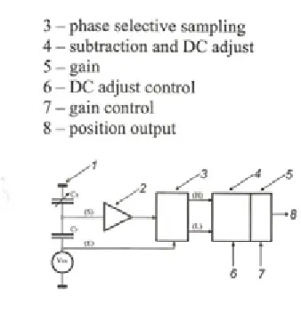
The design o f the electronic part was mainly driven by the demand for a precise and low-noise position-measurement system. To enable simple production o f the mechanical system the beam is electrically connected to the sensor-chip substrate and thus to the ground potential. The noise analysis o f the system indicated that the most effective input structure would, in our case, be a simple capacitive divider, because we are using only one electrode to measure the capacitance. The capacitive divider consists o f the capacitance between the sensing electrode and the grounded beam (Cx) and the excitation signal supplying the capacitor (Cr) connected between the sensing electrode and a source o f the AC signal (excitation signal), as shown in Fig. 3 where the meaning o f the marks is the following: 1 2
1
- grounded cantilever2
- voltage follower system3 - phase selective sampling 4 - subtraction and DC adjust 5 - gain
6
- DC adjust control 7 - gain control8
- position outputFig. 3. Electronical part o f the system
The beam-tip position displacement changes the capacitance o f the sensing electrode to the beam (Cx - capacitor 2) and thus influences the amplitude o f the signal on the node S. It can be described w ith the following:
Us = u ec t
(Cr+Cx) (
4
)where UE is the peak-to-peak value o f the excitation signal. Node S is a node w ith an extremely high impedance, so the voltage o f this node cannot be directly accessed. To observe the voltage o f this node a special patented voltage- follower system was designed, having only a IfF (10‘
15
F) effective input capacitance. This was a key parameter, as the capacitance o f both capacitors in the divider system does not exceed 90fF and a higher follower input capacitance would drastically reduce the available signal.The output o f the voltage follower is further processed in a system where the upper and lower peak values o f the signal are sampled (signals (H) and (L)). The voltage difference o f both signal peaks is calculated in next signal processing step and the DC offset is removed using zero-position adjustment. The electronic position-measurement system thus basically transforms the displacement o f the beam tip to a change in the peak-to-peak voltage o f the divided excitation signal, which is further converted to a direct voltage output by means o f peak-to-peak sampling. The high-level model o f the electronic system must reflect three main parameters o f the real electronic system.
to output voltage. The change in the beam position is reflected in the change o f the peak-to-peak voltage swing on node (S), as described in (4). This parameter is inherent in the system we are using and we can only influence it by changing the mechanical properties o f the system, i.e., the distance o f the beam from the m easurement electrode and the stiffness o f the beam. O f course the improvements in open-loop linearity (bigger distance and stiffer beam) cause a reduction o f the sensitivity, and so the optimum had to be found. The linearity is not a problem in a closed-loop system as it can be greatly improved by the feedback control.
• The second is the delay o f the electronic processing o f the signal. This is mainly dependent on the frequency o f the AC excitation signal, as the peak-to-peak measurem ent system requires at least one clock cycle o f the AC signal to display the correct output value. O f course we want the delay to be as short as possible, especially in the case o f closed-loop realization, due to potential stability problems. For this we have to increase the frequency o f the AC excitation signal, where the limitation is the settling time o f the voltage-follower amplifier.
• The third is the gain (X). For an open- loop measurement system it m ust be chosen so that the output-voltage swing covers the desired measurement range. In the closed-loop configuration it influences the level o f system linearity and signal bandwidth. The obvious limitations are the system stability and the increase o f the noise level in the loop. For a complete system description and simulation the model o f the electrical part has to be merged w ith the model o f the mechanical part, as the properties o f the electrical part can significantly influence the overall system behavior. For this reason we have decided to include in the model description all three m entioned parameters. The non-linearity o f the system is incorporated through (4). The m easurement-system delay, which is equal to one period o f the excitation signal, was taken to be 50 ps, as this is an optimal value coming from transistor-level simulations o f the
measurement electronics [
6
] and [7]. The gain (X) is a param eter that we can choose to suit the system requirements. So the function o f the beam deflection to the output voltage o f the measurement system can be defined as:U oat= K 7 u ec t
C .+
-h + y [ z )
(5)
and the output is sampled every 50 ps. In (5) s is the dielectric constant and A
2
is the area o f the capacitor 2 (see Fig.2).We should mention that the functionality and the desired properties o f the electrical part itself were optimized with a simulation in SPICE [
6
] and [7].1.3 Comparison of the Model to the Measurement Results
The experiments with the prototype samples were divided into observations o f the static and dynamic properties. First, the electrostatic actuator system was used to apply a force to the cantilever. This system uses both capacitors in the middle and at the tip to apply the attraction force to the beam. Since the capacitor beneath the beam tip is also used for the distance measurement, the actuation and measurement function are multiplexed on the same capacitor. This results in a 50% duty ratio o f actuation, which was also included into the model for force calculations. The measurements o f the beam-tip deflection as a result of the electrostatic force are presented in Table 1.
Table 1. Static characteristics o f the combined
system ______________ _______ _______
A c tu a ti o n v o lt a g e [ V ] O u tp u t v o lt a g e [ V ] T ip c a p a c it a n c e v a lu e C a lc u la te d a p p li e d f o rc e o n t h e t ip C a n ti le v e r ti p d is ta n c e t o s u rf a c e R e la ti v e p o s it io n [ n m ]
0 .0 0 .0 0 8 4 .8 6 0 + 1 1 2 2 0 4 0
0 .3 - 0 .1 0 8 5 .0 4 1+11 2 1 9 9 5
0 .6 - 0 .2 8 8 5 .3 7 4 + 1 1 2 1 9 0 14
0 .9 - 0 .9 9 8 6 .7 1 9 + 1 1 2 1 5 7 4 7
1.2 - 1 .7 4 8 8 .1 5 1 7 + 1 2 2 1 2 1 8 3
1.5 - 2 .6 7 9 0 .0 1 2 8 + 1 2 2 0 7 8 1 2 6
1.8 -3 .9 1 9 2 .5 8 4 2 + 1 3 2 0 1 9 1 8 5
2 .1 - 5 .5 8 9 6 .2 5 6 2 + 1 4 1 9 4 3 2 6 1
The actuation voltage in the first column is the voltage applied to the actuation capacitors. The output voltage is the output o f the tip- capacitor measuring system. The third column represents the calculated capacitance value o f capacitor number 2. The fourth column shows the calculated applied force on the cantilever tip from the actuation capacitors and from the measurement system (the excitation voltage used for the capacitance measurement also exhibits electrostatic force). Knowing the characteristics o f the capacitance-measurement electronics the cantilever-tip distance to the silicon surface was then calculated as presented in the fifth column.
The described data were used to improve the static properties o f the mechanical part o f the model. Comparing these results to the model the obvious difference was the starting position o f the cantilever. In the real system the beam was bent back so that the beam tip was 0.5 pm further from the surface than the core o f the beam. This is the result o f residual stress caused by the production procedure o f the cantilever. To implement this in the model we applied a pull-up force along the whole cantilever length, which resulted in the beam bending observed in the measurements. We also made m inor changes to the beam stiffness to fit the model to the measurements. These differences could result from the fact that the beam material was polycrystalline silicon, and from the uncertainty o f the beam thickness.
The dynamic response o f the system was also measured using the actuation voltage as the input stimulus. The actuation voltage was changed step-wise by 350 mV at different DC starting points o f the actuation voltage. The DC starting actuation voltage created an attraction force so the beam position at the start o f each step function (350 mV amplitude) was different for each measurement. The capacitance change at the beam tip, as measured by the position-sensing electronic system, was observed using a digital oscilloscope. The step change in the actuation voltage resulted in an increase o f the attraction force as the capacitor voltage was increased. This additional force required a change in the beam-tip position to compensate the new value o f the electrostatic force with the spring force o f the cantilever. The beam movement was, o f course, damped by the air-damping mechanisms. The oscilloscope shots (as shown in Figs. 4 and
6
) present the time-dependent movement o f the beam tip.These results were compared to the theoretical model. Here, the differences between the model and the measurement results were bigger compared to the static measurements o f the system. The measurement results showed that the damping factor was increased by more than a factor o f two if the cantilever position was moved from 2204 to 1829 nm. This is an even higher ratio than the theoretically calculated factor o f 1.73. This led us to the conclusion to use (in Eq. (3) in denominator) the dimensionless-gap width to the power o f four in our damping calculations.
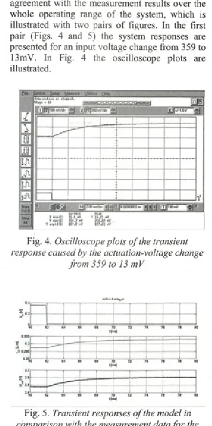
The improved model showed very good agreement with the measurement results over the whole operating range o f the system, which is illustrated with two pairs o f figures. In the first pair (Figs. 4 and 5) the system responses are presented for an input voltage change from 359 to 13mV. In Fig. 4 the oscilloscope plots are illustrated.
Fig. 4. Oscilloscope plots o f the transient response caused by the actuation-voltage change
from 359 to 13 mV
'M
0 3 0 5 f ~ f~— T T--- T — " — f
—L—
Fig. 5. Transient responses o f the model in comparison with the measurement data fo r the
Fig.
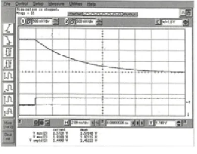
6
. Oscilloscope plots o f the transient response caused by the actuation-voltage changefrom 1.57 to 1.921V
Fig. 7. Transient responses o f the model, in comparison with the measurement data, caused
by the actuation-voltage change from 1.57 to 1.921V
The oscilloscope plots present the response o f the cantilever-tip position-measurement electronics as the upper trace (trace
1
), and the actuation voltage as the lower trace (trace 2). The measurements below show the lower voltage level o f the actuation voltage (Vmin(2)),1
the higher level o f the actuation voltage (Vmax(2)) and the resulting difference of the position- measurement signal (Vam ptd(l)). The input stimuli is a step-voltage change in the actuation voltage and the levels are Vmin(2) and Vmax(2). The time scale in all the plots is 2 ms per division.Fig. 5 is divided into three subplots, where it is possible to observe the applied input voltage (upper part), the movement o f the cantilever tip (middle part) and the corresponding output- voltage signal (lower part) o f the model. In this lower part o f the plot the measurement data from
Fig. 4 are also presented in black color, while model responce is gray. A similar comparison o f the model and the system responses are presented in Fig.
6
and 7 for an input voltage-change from 1.57 V to 1.921 V.We should mention that the simulation o f the described measurement system and the animation o f the mechanical part were realized in Matlab with Simulink [11] and [17].
2 SUMMARY
The model o f the presented micro-mechanical system was a team effort by specialists in the field o f microelectronic design, mechanical design and control. It was developed in a cyclic procedure, where the introduced simplifications made it possible to include the whole system in the same simulation environment. Several iterations were needed because all o f the system properties and parameters were not known in advance.
The starting model was based on theoretical equations and was further improved using measurement data taken from prototype devices. The development o f the model involved two major steps.
The first step covered the static characteristics o f the system resulting from the equilibrium o f the electrical actuation force and the cantilever spring force.
The second step was the introduction o f the dynamic properties governed mainly by air damping mechanisms. The final result has a high degree o f compliance with the actual measurements and has been used for the further development o f the measurement system.
3 REFERENCES
[1] Atanasijević-Kunc, M., Kunc, V., Diaci, J., [9] Karba, R., Modelling and Analysis o f Combined Electronic and Micro M echanical System, Proceedings o f the 4th
IMACS Symposium on Mathematical
Modelling, Troch, I., Breitenecker, F. (ed.), [10]
Vienna, Austria, 2003.
[2] Baschirto, A. Gola, A., Chiesa, E., Lasalandra, E., Pasolini, F., Tronconi, M., Ungaretti, T., A ±-g dual-axis linear [H ] accelerometer in a standard 0.5-pm CMOS technology for high-sensitivity applications,
IEEE Journal o f Solid-State Circuits, July P ^ ]
2003, vol.38, p.1292-1297.
[3] Böser, B. E., Howe, R. T., Surface micromachined accelerometers, IEEE
Journal o f Solid-State Circuits, M arch 1996,
voi.31, p.366-375. [ 131
[4] Daugherty, R. L., Franzini, J. B., Finnemore, E. J., Fluid Mechanics w ith Engineering P ^ ] Applications, McGrow - Hill,
8
th ed., Singapore, 1985.[5] Gola, A., Chiesa, E., Lasalandra, E., P 3] Pasolini, F., Tronconi, M., Ungaretti, T., Baschirotto, A., Interface for MEMS-based rotational accelerometer for HDD Applications with 2.5 rad/s
2
resolution and [16] digital output, IEEE Sensors Journal, August 2003, voi.3, no.4.[
6
] HSPICE, Version H92, Elements and Models, User's M anual, Meta-Software,1992. [17]
[7] HSPICE, Version H92, Analysis and M ethods, User’s Manual, Meta-Software, [18]
1992.
[
8
] IJntema, D. J., Tilmans, H. A. C., Static and dynamic aspects o f an air-gap capacitor,Sensors and Actuators, 1992, A, 35, p. 12
1
-128.
Marco, S., Samitier, J., Herms, A., Morante, J. R., Analysis o f electrostatic - damped piezoresistive silicon accelerometers,
Sensors and Actuators, 1993, A37 - 38,
p.317-322.
Matko, D., Karba, R., Zupančič, B., Simulation and modeling o f continuous systems, A case study approach, Prentice
Hall, 1992.
MATLAB, The Language o f Technical Computing, Version 5, The MathWorks Inc.,
1999.
Matsumoto, Y., Esashi, M., Integrated capacitive accelerometer with novel electrostatic force balancing, Technical
Digest o f the 11th Sensor Simposium, 1992,
p.47-50.
Popov, E. P., Engineering M echanics o f Solids, Prentice H a ll,, 1990, New Jersey. Rudolf, F., Jom od, A., Bencze, P., Silicon microaccelerometer, Transducers'87, 1987, p.395-398.
Rudolf, F., Jom od, A., Bergqvist, J., Leuthold, H., Precision accelerometers with pg resolution, Sensors and Actuators,, 1990, A21-A23, p.297-302.
Siedel, H., Riedel, H., Kolbeck, R., Mtick, G., Kupke, W., Königer, M., Capacitive silicon accelerometer with highly symetrical design, Sensors and Actuators, , 1990, A21- A23, p.312-315.
Simulink, User's Guide, The MathWorks Inc.
1999.
Starr, J. B., Squeeze-film Damping in Solid- State Accelerometers, IEEE Solid-State
Sensor and Actuator Workshop,, June 1990,