Vol. 2 (2012) No. 1 ISSN: 2088-5334
A Methodology for Cell Merging Circuit Transformation on
Post-placement High Speed Design
Diana Tan Hui Lyn
#, Arjuna bin Marzuki
#, Jennifer Lim Min May
* # School of Electrical & Electronic Engineering, Universiti Sains Malaysia,Nibong Tebal, Penang, 14300, Malaysia Email: [email protected], [email protected]
*Intel Microelectronics (M) Sdn. Bhd., Bayan Lepas FTZ, Penang, 11900, Malaysia Email: [email protected]
Abstract— This paper proposes a localize circuit transformation algorithm to further optimize the post-placement netlist in order to improve the overall timing of a design. The proposed algorithm reduces the total cell delay and net delay of timing violation paths by replacing a small group of cells (form up by two to three cells) that are placed close to each other with a functional equivalent standard cell available in the technology library. The algorithm has been implemented and applied to a number of optimized post-placement netlists which have went through conventional post-post-placement circuit transformation optimization processes such as gate relocation, cell re-sizing, repeater insertion and cell replication. The experimental results show that on average, this algorithm is able to further improve the timing of the optimized post-placement netlist by 27.75%, while keeping the design area increase by 0.2%.
Keywords— post-placement optimization, cell merging, circuit transformation, netlist optimization, timing closure.
I. INTRODUCTION
Placement is the intermediate stage between logic synthesis and routing stages in VLSI design flow. It is also the first stage which starts the physical implementation of a design [1]. During this stage, each standard-cell in the gate-level netlist generated by the logic synthesis tool will be assigned an optimized location based on design constraints [1]. With this placement information, netlist can be revisited and optimized with more accurate timing information [2]. Netlist optimization at the post-placement stage is very important as it is able to further optimize the netlist before passing it to routing tool. Besides that, this will also provide a better starting point for routing stage.
During post-placement optimization, placement tool will first analyse the circuit in order to identify all the timing critical paths of the design. Placement tool will then apply a variety of circuit transformation techniques such as gate relocation, cell re-sizing, repeater insertion and cell replication to reduce the negative slacks of these paths [3]. Each of these circuit transformation techniques are explained below.
1) Gate Relocation: In this technique, cells which are connected to a slow net and are placed too far to meet the timing requirement will be selected [3]. These cells will then
be move closer to shrink the span of the net [3]. The advantage of this method is that, it only focus on cells connected to critical and near-critical paths, the run time is greatly reduced compared to performing a new placement, and the optimization is more controllable [4].
2) Cell Re-sizing: The goal of cell re-sizing is to replace cells on the critical and near critical paths with higher power-level cells available in a library which are equivalent in functionality in order to improve timing [5]. This is a very effective timing improving technique. It changes the input capacitances and driving resistances of cells on timing violation paths [4].
3) Repeater Insertion: Repeater serves multiple functions such as:
a) Signal restoration: Repeater is inserted at fixed wire length intervals determined by the technology to cut down delays which grow quadratically with wire length [2].
b) Strengthen the driving strength of a cell: Buffer can be used to increase the drive strength for a cell that is driving a large load [2].
inserted to buffer a portion of the fanouts to minimize the delay [6]. For partition, buffer is used to drive the critical path load so that the driver on the critical path sees only the buffer’s input pin capacitance in place of the high load [2].
4) Cell Replication: In this technique, the driving cell of a net is replaced by two identical replicas, and the fanouts are partitioned into two groups for each replica [4]. Its effect is similar to doubling the driver size, but at the same time it also separate the non-critical fanouts from the critical ones by connecting them to different replicas [4]. This method is more effective than driver up-sizing method when a net has large non-critical load [4].
From the circuit transformation techniques described above, we can see that during post-placement optimization, placement tool tries to adjust the location or the size of cells connected to timing violation paths. Besides that, it also duplicates the high fanout cells or adds repeaters to the timing violation paths in order to reduce the negative slacks of these paths. However, there still exist some timing violation paths which are not able to improve by these circuit transformation techniques. After studying timing reports generated at post-placement optimization stage from a few netlists, we find that a few of these timing violation paths contain small group of cells which are placed close to each other and are optimizable in order to reduce the total cell delay and interconnect delay of the timing violation paths.
In this paper, we present a new circuit transformation algorithm for post-placement netlist and timing optimization. The proposed algorithm optimizes the post-placement netlist base on the placement-based timing analysis result. The algorithm go through all the timing violation paths of the design path by path to look for cells which are placed close to each other and are replaceable with a functional equivalent cell available in the technology library. These groups of cells will then be replaced with their functional equivalent cells respectively. In order to preserve the placement of the design, the cell replacement process is done with ECO (Engineering Change Order) technique. The described algorithm has been implemented and applied to a number of post-placement netlists which have been optimized by the circuit transformation processes described above. Application results show an average of 27.75% of further timing improvement on the post-placement netlist while keeping the area increment of the design by 0.2%.
The rest of the paper is organized into five sections. In Section II, we discuss some placement-based timing analysis concept and standard cell properties in technology library. Our post-placement cell merging circuit transformation optimization algorithm is introduced in Section III. We present some experimental results in Section IV and concluding remarks in section V.
II. PRELIMINARIES
A. Placement-based Timing Analysis
During timing analysis process, timing analyser of the placement tool will compute all the gate and net delay in the design.
a) Standard cell delay: Standard cell delay is a function of the input signal slope and the summation of the capacitance of the output wire and input gates of all cells connected to the output net [7].
b) Net delay: Net delay is a function of the resistance of the metal and the summation of the capacitance of the metal and input gates of all cells connected to the net [7]. In order to have a more accurate prediction of the wire length, global route is done at post-placement stage to outlines how each net will be route in the design. Net length derived from the result of global route will then be used for net delay calculation.
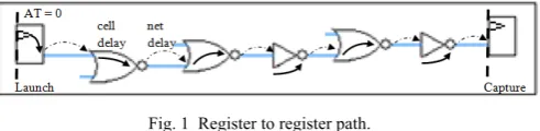
Every path in the design is a register to register as shown in Fig. 1 [8]. Total delay of a path is calculated as the summation of all the net and cell delay from the clock pin of launching register to the data pin of capturing register [8]. The solid timing arc shown in Fig. 1 represents the cell delay whereas the dotted timing arc represents the net delay.
Fig. 1 Register to register path.
In order to identify the timing violation paths in the design, timing analyser in the placement tool calculates the arrival and required times at all points in the network [3]. Arrival time is the absolute time at which all signals actually arrive, whereas required time is the absolute time at which the signals are required to arrive [3]. The difference between required time and arrival time is called slack [3]. Timing paths which contain timing point with negative slack are called timing violation path. All these paths are the subject for optimization.
B. Standard Cell of Technology library
Standard cell of technology libraries are build with complementary CMOS concept [9]. Some properties possess by the standard cell are:
1) Cell area increase as cell fan-in increase
2) Propagation delay increase quadratically with cell fan-in
3) Propagation delay increase linearly with cell fan-out
The propagation delay of a complementary CMOS gate is defined in equation (1).
T
p= a
1FI + a
2FI
2+ a
3FO
(1)
Where FI and FO are the fan-in and fan-out of the gate, respectively, and a1, a2 and a3 are weighting factors that are a
function of the technology [9]. From this equation we can see that, fan-in has significant effect on a gate propagation delay. Gate with fan-in greater than 4 will possesses excessively large propagation delay and must be avoided [9].
C1 is initially charge high. In case (a), C2 and C3 are already
discharge. When signal A changes, only C1 need to be
discharge. In case (b), when signal A changes, C1, C2 and C3
need to be discharge, resulting in a larger delay [9].
Fig. 2 Inference of transistor ordering on delay.
III.OVERVIEW OF PLACEMENT BASED CELL MERGING
CIRCUIT TRANSFORMATION
We propose a placement based cell merging circuit transformation algorithm to improve the overall timing of a design. This algorithm will base on the standard cells available in the technology library, cell’s fanout, as well as the position of each cell in the design to determine the portion of timing violation paths can be merged. This algorithm will first scan through all the timing violation paths’ cells in the design to identify merge-able cell groups (form up by two to three cells). Then it will replace the cells in these merge-able cell groups with a new standard cell with identical functionality.
By merging the cells in the timing violation paths, this algorithm able to further optimize the post-placement netlist hence improve the overall timing of the design. The transformation flow and algorithm are described below in detail.
A. Problem Formulation
Given a mapped and placed netlist which has gone through all the post-placement optimization circuit transformation process such as gate-relocation, cell re-sizing, repeater insertion and cell replication. Our goal is to further optimize the netlist in order to meet the design timing closure.
B. Cell Merging
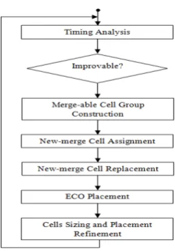
Our proposed circuit transformation algorithm is outlined in Fig 3. After timing analysis, we construct a set of merge-able cell groups along the critical path. A functional equivalent standard cell is then assigned to each merge-able cell group. This functional equivalent standard cell is named as new-merge cell. In the next step, cells inside the merge-able cell group are replaced with the assigned new-merge cell. ECO (Engineering Change Order) placement algorithm is then used to generate a rough placement for the new-merge cells by taking timing constraints into consideration. After that, new-merge cells as well as all the cells connected adjacent to it will be sized appropriately and placement of these cells will then be refined. This algorithm iterates until the design has no more room for further improvement.
Fig. 3 Cell merging circuit transformation algorithm overview.
1) Timing Analysis: The first step of our algorithm is to perform timing analysis to identify all the critical paths in the design. Critical paths are the data paths which fail to meet the design timing constraints. These paths will become the subject of the subsequent cell merging circuit transformation algorithm.
2) Merge-able Cell Group Construction: In this section, we introduce our merge-able cell group construction algorithm. This algorithm will go through every cell of the critical paths and base on the level of complexity, fanout as well as the position of each cell to construct a set of merge-able cell group along the critical path. Each merge-merge-able cell group will only contains two to three cells. The cells inside the merge-able cell group are the targets for merging.
In this experiment we divide the standard cells of the data path library into four groups according to the level of complexity of the cell.
a) Basic Cell: This group contains three fundamental logical cells, from which all other functions, no matter how complex, can be derived. These logical cells are NOT gate, 2-input NAND gate and 2-input NOR gate.
b) Complex Cell: Logical cell with functionality derivable with two to three basic cells belong to this group. Some example of complex cells are input NAND gate, input NOR gate, input AOI (AND-OR-INV) gate, etc. 3-input NOR gate can be derived by two 2-3-input NOR gate and one NOT gate. 3-input NAND gate can be derived by two 2-input NAND gate and one NOT gate. 3-input AOI gate can be derived by one 2-input NAND gate, one 2-input NOR gate and one NOT gate.
c) Very Complex Cell: This group contains logical cells with functionality derivable with one complex cell and one to two basic cells. Some example of very complex cells are 4-input NAND gate, 4-input OAI (OR-AND-INV) gate, etc. 4-input NAND gate can be derived by one 3-input NAND gate, one 2-input NAND gate and one NOT gate. 4-input OAI gate can be derived by one 3-input NOR gate, one 2-input NAND gate and one NOT gate.
d) Ultra Complex Cell: The rest of the datapath library cells which do not belong to the above three categories will be fall into this category. The functionality derivation of ultra complex cell into three cells will involve at least a very complex cell. Cells belong to this categories will not be used for merging algorithm as the netlist represented by the cells is already optimized and over optimize a netlist will make the timing of the design worst. Besides that, cells belong to this category also possess bigger area. Using too much Ultra complex cell in the design may violate the design area constraint.
Next, we find out all the possible two to three cells combination, form up by basic and complex cells, for each complex and very complex cell of the datapath library. Any of these cells combination found in the critical paths will be group together. These combination groups will then be subject for interconnect analysis.
In interconnect analysis, all the interconnect nets between the cells of the combination groups will be analyze. Only combination groups with all its interconnect nets with only one fanout will be keep for further analysis. Fig. 4 shows a small netlist which contains three combination groups A, B and C. The interconnect nets of these combination groups are highlighted with a thicker wire. As combination group A and B contain an interconnect net with fanout equal to two, therefore these two combination groups will be remove and only combination group C will be keep for further analysis.
Fig. 4 Merge-able cell group construction.
After filtering out combination groups with interconnect nets more than one fanout, the remaining combination groups will be subjected to driver-receiver distance analysis. In driver-receiver distance analysis, we will first identify the drivers and receivers of the combination group. In Fig. 4, drivers of combination group C are two NOT gates and a NOR gate. Whereas the receivers of this group are a NOT gate and a flop register. The location of these drivers and receivers will be identified and distance between the drivers and receivers will be calculated. Combination groups with maximum distance between drivers and receivers more than a certain distance will be removed. The distance is determined by the optimum wire length of the highest metal layer used in the design. The combination groups which remain after interconnect and driver-receiver distance analyses are named as merge-able cell groups.
3) New-merge Cell Assignment: Each merge-able cell groups on the critical paths will be mapped to its respective complex or very complex cell. The mapped cells for each merge-able cell groups are named as new-merge cells for the design. Fig. 5 shows an example of merge-able cell group with its new-merge cell.
Fig. 5 (a) Merge-able cell group. (b) New-merge cell.
4) New-merge Cell Replacement: In order to replace the merge-able cell group with new-merge cell, we first need to identify all the inputs, outputs and interconnect nets of the merge-able cell group. Next, we remove all the cells of the merge-able cell group as well as its interconnect nets and replace it with its new-merge cell. Lastly, we connect the inputs nets of the merge-able cell group to the input pins of new-merge cell and output net of the merge-able cell group to output pin of new-merge cell.
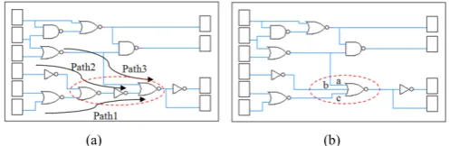
Fig. 6(a) shows a small netlist with a merge-able cell group and Fig. 6(b) shows the resultant netlist after new-merge cell replacement process. Replacing the new-merge-able cell group with its assigned new-merge cell helps in improving the timing of path 1 and 2 as total number of cell delay as well as the net delays of these two paths have been reduced. However, this merging process might cause a slight increase in the total delay of path 3 even though there are no changes in the total number of cells in this path. This is because under the condition of same input signal slope and output pin load, gate with higher level of complexity might possess higher gate delay.
Fig. 6 Replacement of merge-able cell group with new-merge cell
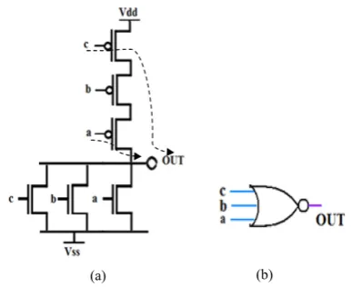
While improving the timing of critical paths which contain merge-able cell groups (e.g. path 1 and 2 in Fig. 6(a)), it is important to preserve timing of other paths (e.g path 3 in Fig. 6(a)) which are timing dependent to the critical paths. Two timing paths are said to be timing dependent if timing optimization of one of these paths can change the timing information of the other path, due to their sharing of logic. As explained in section II, all input pins of a standard cell possess different in-to-out delay. Input pin which is closer to the output pin of a gate possess smaller in-to-out delay. Therefore, by connecting the input nets of merge-able cell groups which come from the timing dependent path to the input pins of new-merge cell which is closer to the output pin help to preserve the timing of timing dependent paths. Fig. 7 shows the transistor level and symbolic view of the new-merge cell (3-input NOR gate) of Fig. 6. Pin a of this gate possesses lesser delay than other pins as it is closer to the output pin of the gate. Therefore, input net from path 3 of the netlist shown in Fig. 6(a) need to be connected to the pin a of the new-merge cell.
(a) (b)
Fig. 7 (a) Transistor level of NOR gate. (b) Symbolic view of NOR gate.
5) ECO Placement: After new-merge cell replacement process, ECO placement technique is used to generate a rough placement for new-merge cells by taking timing constraints as well as location of merge-able cell group into consideration. Fig. 8(a) shows an example of physical view of merge-able cell group’s cells and its boundary. Boundary location of merge-able cell group is determined by the maximum and minimum boundary of its cells. Each new-merge cell must be placed at location within or closest to merge-able cell group boundary. Fig. 8(b) shows the resultant placement location of new-merge cell for merge-able cell group shown in Fig. 8(a).
Fig. 8 Physical view of the circuit in Fig. 6. (a) Merge-able cell group. (b) New-merge cell.
6) Cell Sizing and Placement Refinement: Lastly, new-merge cells as well as all the cells connected adjacent to it will be sized appropriately. After cell sizing, placement of cells in the design will be refine to make sure all the cells are in row and there are no overlapping of cells in the design.
IV.EXPERIMENTAL RESULTS
Our cell merging circuit transformation algorithm is technology independent. The only thing needs to be taken care of while applying this algorithm to designs running with different technology is the acceptable maximum distance between drivers and receivers of combination groups which can be categories as merge-able cell group during the distance analysis step at merge-able cell group construction stage of our algorithm. In this experiment, we have implemented our cell merging circuit transformation algorithm on a number of post-placement netlists obtained from industry, which run at 3.6 GHz with 22 nm technology libraries. All these netlists have been passed through all the
conventional post-placement circuit transformation optimization process such as gate relocation, cell re-sizing, repeater insertion and cell replication.
The placement tool which we used in this experiment is IC Compiler, Version D-2010.03-ICC-SP1-1. In order to test the algorithm, we have written the algorithm in tcl script. This script is then sourced into the placement tool and the algorithm is integrated into the conventional placement flow at post-placement optimization stage.
The experimental results are shown in Table I. This table shows the total negative slack (TNS) and design area of each circuit’s post-placement netlist optimized with:
a) conventional post-placement circuit transformation techniques (conventional)
b) conventional post-placement circuit transformation techniques and cell merging circuit transformation techniques (conventional+CM)
The result shows an improvement in all the netlist with TNS reduction ranging from 14.38% to 43.62%. On average, we are able to further improve the post-placement netlist timing by 27.75%, while keeping the design area increment by 0.2%.
V. CONCLUSION
We have presented a new post placement circuit transformation optimization algorithm named as cell merging. This algorithm further optimize the timing violation paths of post-placement netlist by identify the merge-able cell groups in the paths andreplace it with a functional equivalent standard cells available in the datapath technology libraries. Cell merging algorithm able to reduce the total cells delay and nets delay of a timing violation path, hence improve the timing of the timing violation path. As this algorithm only performs localize optimization, therefore only the cells belong to merge-able cell groups will be affected. The rest of the design will be preserved. Experimental results show an average of 27.75% of further timing improvement on the post-placement netlist while keeping the area increment of the design by 0.2%.
ACKNOWLEDGMENT
We would like to thanks Intel Penang Design Center for providing us the IC Compiler license and netlists for this experiment.
REFERENCES
[1] I. Fudos, X. Kavousianos, D. Markouzis and Y. Tsiatouhas, “Placement and Routing in Computer Aisded Design of Standard Cell Arrays by Exploiting the Structure of the Interconnection Graph”, Computer-Aided Design and Applications, CAD Solutions, LLC, 2008.
[2] O. Coudert, “Timing and Design Closure in Physical Design Flows”, IEEE, 2002.
[3] J.Kim, M.C.Papaefthymiou, and J.L. Nevew, “Parallelizing Post-Placement Timing Optimization”, IEEE, 2006.
[4] H. Ren and S. Dutt, “Algorithms for Simultaneous Consideration of Multiple Physical Synthesis Transforms for Timing Closure”, ACM/IEEE Design Automation Conference, 2008.
[5] K. Sato, M. Kawarabayashi, H. Emura and N. Maeda, “Post-Layout Optimization for Deep Submicron Design”, 33rd Design Automation Conference, 1996.
[6] L.N. Kannan, P. R. Suaris and H. G. Fang, “A Methodology and Algorithms for Post-Placement Delay Optimization”, 31st ACM/IEEE Design Automation Conference, 1994.
(a) (b)
[7] J. Rernard, (2011) “Physical level Design using Synopsys”. Scholarly paper, George Mason University.
[8] G. Micheal, “PrimeTime Static Timing Anlaysis Tool”, Scholarly paper, George Mason University,2006.
[9] J. M. Rabaey, A. Chandrakasan, and B. Nikolic, “Digital Integrated Circuits – A Design Perspective”, Second Edition.
TABLE I.
POST-PLACEMENT CELL MERGING TIMING OPTIMIZATION RESULTS
Circuit Gates Design Area, µm Total Negative Slacks (TNS), ns
Conventional Conventional+CM Improvement, % Conventional Conventional+CM Improvement, %
Circuit 1 19.5k 27191.4 27274.2 -0.30 -0.2230 -0.1415 36.65
Circuit 2 39.4k 48543.4 48801.8 -0.53 -1.2918 -1.0667 17.43
Circuit 3 4.1k 5059.4 5063.1 -0.07 -0.5380 -0.3760 30.11
Circuit 4 9.0k 11176.5 11187.9 -0.10 -0.1557 -0.1179 24.28
Circuit 5 8.5k 10933.8 10945.3 -0.11 -0.0337 -0.0190 43.62
Circuit 6 8.5k 11010.4 11020.9 -0.09 -0.0605 -0.0518 14.38