RESEARCH NOTE
MODELING OF SUBSTRATE NOISE IMPACT ON A
SINGLE-ENDED CASCODE LNA IN A LIGHTLY DOPED SUBSTRATE
S. Aghnout* and N. Masoumi
Department of Electronics, School of Electrical and Computer Engineering
University College of Engineering, University of Tehran, P.O. Box 14395-515, Tehran, Iran [email protected] - [email protected]
*Corresponding Author
(Received: July 24, 2008 – Accepted: November 5, 2009)
Abstract Substrate noise generated by digital circuits on mixed-signal ICs can disturb the sensitive analog/RF circuits, such as Low Noise Amplifier (LNA), sharing the same substrate. This paper investigates the adverse impact of the substrate noise on a high frequency cascode LNA laid out on a lightly doped substrate. By studying the major noise coupling mechanisms, a new and efficient modeling method is proposed to predict, prior to processing, the LNA performance degradation due to the substrate noise. Our simulations prove that the model can estimate the magnitude of the spurious signals appearing at the output spectrum of the 5 GHz LNA, within an acceptable error of 13%.
Keywords CMOS Integrated Circuits, Mixed Signal IC, Substrate Noise, LNA
هﺪﻴﻜﭼ
ﻢﻴﺳﻖﻳﺮﻃزالﺎﺘﻴﺠﻳديﺎﻫراﺪﻣزاﻲﺷﺎﻧﻲﻧزﺪﻴﻠﻛﺰﻳﻮﻧ،ﻂﻠﺘﺨﻣلﺎﻨﮕﻴﺳﻊﻤﺘﺠﻣيﺎﻫراﺪﻣرد ﻐﺗيﺎﻫ
ﻪﻳﺬ
ﻲﻣلﺎﻘﺘﻧاكﺮﺘﺸﻣﻲﻧﻮﻜﻴﻠﻴﺳﻪﻳﻻﺮﻳزو
ﺖـﻳﻮﻘﺗﻪـﻠﻤﺟزاسﺎـﺴﺣگﻮﻟﺎـﻧآوﻻﺎﺑﺲﻧﺎﻛﺮﻓيﺎﻫراﺪﻣﻲﻳارﺎﻛوﺪﺑﺎﻳ
هﺪﻨﻨﻛ ﻲﻣﺶﻫﺎﻛارﺰﻳﻮﻧﻢﻛيﺎﻫ ﺪﻫد
.
ﻢﻛهﺪﻨﻨﻛﺖﻳﻮﻘﺗﻚﻳدﺮﻜﻠﻤﻋﺮﺑﻪﻳﻻﺮﻳزﺰﻳﻮﻧبﻮﻠﻄﻣﺎﻧتاﺮﺛاﻪﻟﺎﻘﻣﻦﻳارد
ﺎﺧﺎﻧﺖﻈﻠﻏﺎﺑﻪﻳﻻﺮﻳزﻚﻳيورﺮﺑﻻﺎﺑﺲﻧﺎﻛﺮﻓيرﺎﺸﺑآﺰﻳﻮﻧ
ﻲـﻣراﺮـﻗﻲـﺳرﺮﺑدرﻮـﻣﻢﻛﻲﺼﻟ دﺮـﻴﮔ
. ﻪـﻌﻟﺎﻄﻣﺎـﺑ
ﻢﺴﻴﻧﺎﻜﻣ لﺪﻣشورﻚﻳ،ﻪﻳﻻﺮﻳزﺰﻳﻮﻧﻖﻳرﺰﺗﻲﻠﺻايﺎﻫ ﻲﻣﻲﻓﺮﻌﻣﺪﻣآرﺎﻛوﺪﻳﺪﺟيزﺎﺳ
ﻲﻣﻪﻛددﺮﮔ
ﺶﻴـﭘﺪﻧاﻮﺗ
ﺶﻴﭘارﻪﻳﻻﺮﻳزﺰﻳﻮﻧزاﻲﺷﺎﻧﻲﺒﻳﺮﺨﺗتاﺮﺛا،ﺰﻳﻮﻧﻢﻛهﺪﻨﻨﻛﺖﻳﻮﻘﺗراﺪﻣﺖﺧﺎﺳزا ﺪﻨﻛﻲﻨﻴﺑ
.
ﻪﻴﺒﺷ يزﺎﺳ
نﺎـﺸﻧﺎـﻫ
ﻲﻣ لﺪﻣﻪﻛﺪﻫد لﺎﻨﮕﻴﺳﻲﮔرﺰﺑهﺪﺷﻪﺋارا
ﺖـﻳﻮﻘﺗﻲﺟوﺮﺧﻒﻴﻃرددﻮﺟﻮﻣ،ﻪﻳﻻﺮﻳزﺰﻳﻮﻧزاﻲﺷﺎﻧﻪﺘﺳاﻮﺧﺎﻧيﺎﻫ
ﺰﻳﻮﻧﻢﻛهﺪﻨﻨﻛ
5
زاﺮﺘﻤﻛيﺎﻄﺧﺎﺑوﻲﺘﺳردﻪﺑار،ﺰﺗﺮﻫﺎﮕﻴﮔ
13
ﻲﻣﻦﻴﻤﺨﺗﺪﺻرد ﺪﻧز
.
1. INTRODUCTION
In recent years, the market of wireless applications has grown enormously, driven by the development of high-performance low-cost CMOS technologies. This CMOS evolution allows the integration of an increasing amount of digital and analog functions on a single die, enabling cost and power reduction [1]. A serious drawback of this single-chip solution is the coupling of the digital switching noise via the common substrate to the sensitive analog circuits, which degrades the overall system performance, sometimes resulting in a failure of the system.
Since a LNA is generally considered to be the most sensitive block in a typical RF receiver, it is a good choice for characterizing the effect of the
substrate noise coupling [2]. Up to now, some experimental research has been done for LNAs mainly for heavily doped substrates. Also, a first study comparing measurements and simulations for a LNA circuit in both heavily and lightly doped substrates has been reported [2]. But these studies don’t offer an applicable model to predict the substrate noise effects on the LNA, in the early stages of design. Moreover, they ignore the capacitive behavior of the substrate in high frequency domain [2,3].
network, using the electromagnetic software IE3D [5]. It is clear that to control the substrate noise coupling problem and guarantee the first silicon success, a systematic approach is mandatory. As such, this paper aims at developing an efficient analytical modeling method that can facilitate the estimation of the substrate noise effects in the early stages of a design.
2. LNA PERFORMANCE DEGRADATION DUE TO SUBSTRATE NOISE
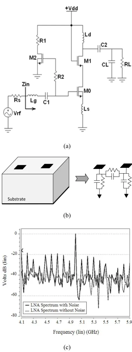
Figure 1a depicts a LNA circuit designed to operate at 5 GHz [4]. A single-ended cascode architecture with an inductive source degeneration has been used because it provides a superior noise performance compared to other single-ended topologies [2]. To study the substrate noise impact, we have drawn the LNA layout and placed a 30 µm × 30 µm square contact 200 µm far from the LNA to represent the fast switching digital part of the integrated circuit. The substrate noise signal will be applied through this contact as the noise injector.
Next, the layout is imported to IE3D. It extracts a three dimensional resistive-capacitive network between fourteen contacts which include the square contact and the different components of the LNA circuit. In IE3D extractions, the substrate is defined as a lightly doped p-type substrate with a resistivity of ρ = 10 Ω. cm and a thickness of 250 µm. It uses a metal backplane at the bottom, which reduces the substrate noise harmful effects [6]. The substrate model includes vertical impedances, between the layout contacts and the backplane, and horizontal impedances, between the square contact and the other thirteen ones. A typical substrate model between two simple contacts is shown in Figure 1b. Now, the substrate model is included in the LNA net list as a subcircuit. As we know, the signals in digital circuits are fast switching square-shape pulses. They inject the substrate noise via the junction capacitances which transmit through the substrate impedances. Because of differential function of the junction capacitances, it is reasonable to suppose the substrate noise as an impulse-form signal. Now, the input RF signal, a sinusoidal of the frequency 5 GHz and the amplitude 10 mV, and the substrate noise, an impulse of the
(a)
Substrate
(b)
(c)
frequency 100 MHz and the amplitude 50 mV, are applied. As Figure 1c illustrates, the substrate noise causes many spurious tones to appear in the LNA output spectrum.
By changing the frequency of substrate noise, both harmonic and intermodulation (IM) tones are observed at the LNA output. The harmonic tones appear at the frequencies which are multiples of the substrate noise frequency. The tones, appearing between harmonics, are IM products arising from the first and the second harmonics of the noise mixing with the 5 GHz RF carrier.
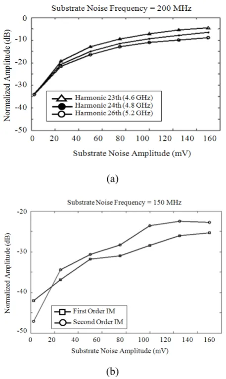
For example as Figures 2a and b show, by increasing the substrate noise amplitude, both harmonic and intermodulation tones increase. Our
extensive simulation results indicate that the IM products are more than 10 dB lower than the harmonic tones. Therefore, the IM products can be ignored without a loss of accuracy.
3. SUBSTRATE NOISE COUPLING MECHANISMS AND MODELING
Switching noise, which is generated by a digital part, travels through the substrate in all directions. Near the LNA circuit, it couples to different components and then couples to the output port, disturbing the output signal.
In the RF CMOS 0.18 µm technology, used for RF applications, any passive or active element is defined as a subcircuit which has one or two terminals to be connected to the substrate model. Meanwhile, the subcircuits of the resistors, capacitors and inductors are connected to the substrate, capacitively. In contrast, the substrate noise couples to the transistors mainly through the bulk node causing threshold voltage variations.
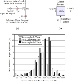
As a result, the MOS transistors may be more severely affected by the substrate noise than the passive devices. On the other hand, the bulk node of M1 is shorted to the ground through the bonding wires which lowers the influence of the substrate noise, seriously. In contrast, as Figure 1a shows, the source nodes of M0 and M2 are shorted to the bulk node where the substrate noise directly couples to them. The above discussion indicates that the dominant substrate noise coupling mechanism is through M0 and M2. Our simulation results, reported in the next section, validate this fact.
As Figure 3a depicts, the substrate noise coupled to the bulk node of M0 can be treated as a series voltage in the source node. Furthermore, the substrate noise coupled to the bulk node of M2 couples to the LNA input port and can be equated as a series noise voltage source in the gate of M0. The ac component of the drain current, id, for a MOSFET in saturation, when the bulk and the source nodes are shorted, is given by [2]:
) T V CS V ( 2
2 gs b m g gs m g ) gs ( F d i
(1)
Where, gm and gmb are the small-signal transconductances from the gate and the bulk to the (a)
(b)
drain, respectively. VGS is the gate-source voltage and VT is the threshold voltage. Therefore, considering Figure 3a, the ac component of the drain current of M0 can be written as:
. ) n2 n1 RF ( F d
i (2)
Where vn1 and vn2 are the substrate noise coupled to the bulk nodes of M0 and M2, respectively. Using Equation 1, id is expressed as:
. ) T V GS V ( 2 n 1 n b m g ) T V GS V ( 2 n RF b m g ) T V GS V ( 1 n RF b m g ) T V GS V ( 2 2 2 n b m g ) T V GS V ( 2 2 1 n b m g ) T V CS V ( 2 2 RF b m g 2 n m g 1 n m g RF m g d i (3)
As a first approximation assuming vn1≈vn2, so that gmbvRF (vn1-vn2)/(VGS-VT)≈0 we obtain
. ) T V GS V ( 2 n 1 n b m g ) T V GS V ( 2 2 2 n b m g ) T V GS V ( 2 2 1 n b m g 2 n m g 1 n m g ( ) T V GS V ( 2 2 RF b m g RF m g d i (4)
Finally, it proves
). n2 n1 ( F ) RF ( F ) n2 n1 RF ( F d
i
(5)
Equation 5 simply models the effects of the substrate noise on the LNA. If we confirm that the coupling through M0 and M2 is the dominant mechanism by which the substrate noise affects the LNA, (this will be shown in the next section) Equation 5 demonstrates that how the LNA amplifies the substrate noise. As a result, as depicted in Figure 3b, a LNA can be modeled as a linear system in terms of its input signals: the RF input and the substrate noise.
4. SIMULATION RESULTS
To prove the validity of Equation 5, that is, linear functionality of the output of the LNA versus its input signals, we have performed three sets of simulations. In all of them, the input RF signal is a sinusoidal of the frequency 5 GHz and the amplitude 10 mV.
In the first simulation set, considered as the reference data, the LNA circuit including the substrate model is simulated where the input RF and the sinusoidal substrate noise signals are applied. The amplitude of the main output signal and the spurious tones are measured versus the substrate noise frequency in the range 20 MHz to 4.5 GHz for three different amplitudes 30 mV, 100 mV, and 200 mV (Figure 3c).
In the second simulation set, the LNA is simulated without including the substrate model, where the noise signals, vn1 and vn2, are set to zero, and then the amplitude of the output signal is measured.
Finally, in the third simulation set, the LNA circuit including the substrate model is simulated where the input RF signal is set to zero and only the sinusoidal substrate noise is applied. In this case, to identify the most critical components which affect the output spectrum due to the substrate noise, a modified substrate model is used. As such, all of the substrate model horizontal impedances are removed except those connecting the square contact to the bulk nodes of M0 and M2. The substrate noise is thereby prevented from traveling to any of the LNA components except M0 and M2. Finally, the amplitudes of the output spurious tones are measured in a wide frequency range of the noise and for several noise amplitudes. Eventually, using the superposition law, the total output is computed by adding the results obtained from the second and third simulations. Now the latter results are compared to those obtained from the first case, in order to validate the linear functionality of the circuit as proposed in this article.
M2, and second, the LNA functions linearly against the substrate noise coupled to M0 and M2.
5. CONCLUSION
We have proposed a new model to predict, prior to processing, performance degradations of a single-ended cascode LNA due to the substrate noise. The model has been validated analytically and through simulations for a 5 GHz single-ended cascode LNA in a 0.18 µm RF CMOS process on a lightly doped substrate. The simulations verify that the model accurately predicts the level of the spurious
signals appearing at the LNA output, due to the substrate noise.
The proposed methodology facilitates estimation of substrate noise effects in the early stages of a design. As verification, we have shown that for several magnitudes of the substrate noise and within a wide range of frequency the accuracy of the results is better than 87 %.
6. REFERENCES
1. Soens, Ch., Der Plas, G.V., Wambacq, P., Donnay, S., and Kuijk, M., “Performance Degradation of LC-Tank
(a) (b)
(c)
VCOs by Impact of Digital Switching Noise in Lightly Doped Substrates”, IEEE JSSC, Vol. 40, No. 7, (July
2005), 1472-1481.
2. Hazenboom, S., Fiez, T.S. and Mayaram, K., “A Comparison of Substrate Noise Coupling in Lightly and Heavily Doped CMOS Processes for 2.4-GHz LNAs”,
IEEE JSSC, Vol. 41, No. 3, (March 2006), 574-587.
3. Xu, M., Su, D.K., Shaeffer, D.K., Lee, T.H. and Wooley, B.A., “Measuring and Modeling the Effect of Substrate Noise on the LNA for a CMOS GPS Receiver”, IEEE
JSSC, Vol. 36, No. 3, (March 2001), 473-485.
4. Kalantari, F. and Masoumi, N., “A Fully Integrated Dual-Band CMOS LNA for IEEE802.16a”, IEICE Electronics Express, Vol. 3, (2006), 474-479.
5. Zeland Software, “IE3D User’s Manual”, Zeland Software, Inc., Release 6, (1999).
6. Joardar, K., “A Simple Approach to Modeling Cross-Talk in Integrated Circuits”, IEEE JSSC, Vol. 29,