HIGH SPEED FULL SWING CURRENT MODE BICMOS
LOGICAL OPERATORS
Arash Ghorbannia Delavar
Islamic Azad University, Science and Research Branch Computer Engineering, Shahid Beheshti University
P.O. Box 14515/775, Tehran, Iran [email protected]
Keivan Navi* and Omid Hashemipour
Department of Electrical and Computer Engineering, Shahid Beheshti University P.O. Box 14515/775, Tehran, Iran
[email protected] - [email protected]
*Corresponding Author
(Received: October 19, 2006 – Accepted in Revised Form: September 13, 2007)
Abstract In this paper the design of a new high-speed current mode BiCMOS logic circuits is proposed. By altering the threshold detector circuit of the conventional current mode logic circuits and applying the multiple value logic (MVL) approach the number of transistors in basic logic operators are significantly reduced and hence a reduction of chip area and power dissipation as well as an increase in speed is achieved. Simulation with HSpice using BSIM 3V3 model and experimental 65nm BiCMOS technology were carried out for speed, and power consumption considerations at different supply voltage levels. Finally the performance of the proposed circuit is compared to an 8 bit voltage mode adder.
Keywords BiCMOS, Multiple Valued Logics, Low Voltage, Threshold Detector
ﻩﺪﻴﻜﭼ
ِِﺍﺭﺩ ﻳ
ِِﻘﻄﻨﻣﺕﺍﺭﺍﺪﻣ،ﻪﻟﺎﻘﻣﻦ ﻲ
ﺮﺳ ﻳ
ﺮﺟﺪﻣﻊ ﻳ
ﮊﻭﺍﻮﻨﮑﺗﺯﺍﻩﺩﺎﻔﺘﺳﺍﺎﺑﻥﺎ ﻱ
BiCMOS ﻪﺋﺍﺭﺍ
ﺖـﺳﺍﻩﺪـﺷ
. ﺎـﺑ
ﺎﻫﺵﻭﺭﻝﺎﻤﻋﺍ ﻱ
ﺭﺎﮐﻭﻩﺩﺎﺳ ﺁ
ﺪﻣ
، ﺰﻧﺍﺮﺗﺩﺍﺪﻌﺗ ﻳ
ﺭﻮﺘﺴ ﺎﻫ
ﺶﻫﺎﮐ
ﻪﺘﻓﺎﻳ ﺑﻭ ﺪﻳ
ـﺳﻭﻦ ﻴ
ﺎـﮐﻪﻠ
ﮕﻤﺸـﭼﺶﻫ ﻴﺮ
ﻱ
ﻥﺍﻮـﺗﺭﺩ
ﻓﺮﺼﻣ ﻲ
ﻨﭽﻤﻫﻭﻪﺷﺍﺮﺗﺖﺣﺎﺴﻣﻭ ﻴ
ﻦ ﺍﺰﻓﺍ ﻳ
ﺖﻋﺮﺳﺶ
ﻪﺑ
ﺖﺳﺩ ﺖﺳﺍﻩﺪﻣﺁ
. ﺩﺪﻌﺘﻣﯼﺯﺎﺳﻪﻴﺒﺷﺎﺑ ۶۵
ﺰـﻴﻧﯼﺮﺘﻣﻮﻧﺎﻧ
ﺡﻮﻄﺳﻪﺑﺖﺒﺴﻧﻪﻳﺬﻐﺗﻊﺒﻨﻣ
ﮊﺎﺘﻟﻭ
ﺶﻫﺎﮐ ﻪﺘﻓﺎﻳ
ﻭ
ﺎﮐﻥﺎﻳﺎﭘﺭﺩ
ﻩﺩﺍﺩﺶﻳﺍﺰﻓﺍﻥﺎﻳﺮﺟﺪﻣﺕﺍﺭﺍﺪﻣﯽﻳﺍﺭ
ﻩﺪﺷ
ﻭ
ﺎﺑ ﻊـﻤﺟ
ﻩﺪﻨﻨﮐ Bit ۸ ﮊﺎﺘﻟﻭﺪﻣ ﺰﻴﻧ ﺖﺳﺍﻩﺪﺷﻪﺴﻳﺎﻘﻣ
.
1. INTRODUCTION
In the early 1970s, NMOS technology was the most feasible, and dominant digital VLSI technology. It retained its status until the late 1970s where a gradual switch to CMOS technology was observed. Memories and microprocessors were widely fabricated using CMOS technology. In the mid- 1980s, the need for higher speed resulted in the introduction of BiCMOS technology as an alternative to CMOS in some applications. The high drive capability of BiCMOS circuits was the main attraction compared to the cheap CMOS alternative. Many high-speed BiCMOS circuits have been fabricated
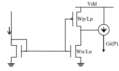
Wn/Ln Wp/Lp Vdd
Gi(P)
Figure 1. Gi circuit realization.
TABLE 1. 0.065 µm Technology Parameters.
NPN
Ft (GHz) 55
Fmax (GHz) 110
Gm/Gce @We-min 1200 CMOS
Vdd (V) 3.3/1
Lmin (nm) 65
Resistors Rs (ohm/sq) 100
Capacitor C (fF/mm2) 3
Routing # Layers 6
Top Metal Thickness (um) 2.5 In part 2 the MVL current mode circuits are
introduced and their benefits are explained and shown. In part 3, current mode circuits and their difference with voltage mode circuits and the principal of threshold detectors are described. Finally, in part 4 the actual proposed current mode circuit is illustrated and comparative simulation results are presented.
2. MVL CURRENT MODE CIRCUITS
MVL is a potential and actual alternative to Binary logic [8-10]. In MVL, instead of having a digit set comprising {0,1} in radix 2, one can define any other greater digit set for example {0,1,2} in radix 3 or as another example {-2,-1,0,1,2} in radix 4. The MVL circuits are generally operated in two modes of voltage or current.
In the current mode the algebraic sum is done linearly by KCL law, it is enough to connect any arbitrary number of wires and in the connecting node one can obtain the algebraic sum of input currents. This property leads to some very efficient circuits. The threshold detector (TD) circuit is an important decision making part of the MVL current mode circuit. The TD can be implemented by a Greater than (Gi) and less than (Li) function as
described below:
Xj∈ (0, 1), X ∈ (0,1,2,…,m-1)
Xj = 1 IF X = j, Xj = 0 IF X ≠ j
Gj, Lj∈ (0,1), X ∈ (0,1,2,…,m-1)
Gj (x) = 1 IF X > j else = 0
Lj (x) = 1 IF X ≤ j else = 0
Based on previous work [4-10] and the simulation results presented, as shown in Figure 1 it can be generally concluded that, changing the ratio of (W/L)pu to (W/L)pd in CMOS inverter gates and using a PMOS transistor as a current source or NMOS as current sink, voltage can be converted to current by applying threshold detector circuits. 0.065 µm BiCMOS technology has been used here. Table 1 illustrates its related parameters.
The functions of the threshold detectors are to differentiate between different levels of current and hence multi levels of logic can be specified. Figure 1 also demonstrates the realization of Gi functions. The output of this detector is connected to a PMOS transistor gate for converting the output voltage to the current.
Tables 2a through 2c specify the different required W/L ratios of transistors for specified current levels.
Tables 3a to 3c show the delay in applying G0 to G2.
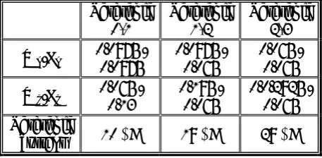
TABLE 2a. Sample of Detector for Threshold Level 0.
Threshold 0-1
Threshold 1-2
Threshold 2-3 Wn/Ln 0.065 / 0.065 0.065 / 0.065 0.065 / 0.0975
Wp/Lp 0.065 / 0.065 0.065 / 0.065 0.065 / 0.065
Threshold
current 10 μA 30 μA 50 μA
TABLE 2b. Sample of Detector forTthreshold Level 1.
Threshold 0-1
Threshold 1-2
Threshold 2-3 Wn/Ln 0.065 / 0.065 0.0975 / 0.065 0.065 / 0.065
Wp/Lp 0.065 / 0.0975 0.065 / 0.0975 0.39 / 0.065
Threshold
current 21μA 40 μA 62 μA
TABLE 2c. Sample of Detector forTthreshold Level 2.
Threshold
0-1 Threshold 1-2 Threshold 2-3 Wn/Ln 0.0975 / 0.0975 0.0975 / 0.065 0.065 / 0.065
Wp/Lp 0.065 / 0.13 0.195 / 0.065 0.0.2925 / 0.065
Threshold
current 10 μA 19 μA 29 μA
TABLE 3a. Testing Delay Circuits for Level 0.
Test Circuit Tdr (Rising Edges)
Tdf (Fanning Edges)
G0 0.21 ns 0.1 ns
G1 0.17 ns 0.23 ns
G2 0.2 ns 0.37 ns
TABLE 3b. Testing Delay Circuits for Level 1.
Test Circuit Tdr (Rising Edges)
Tdf (Fanning Edges)
G0 0.14 ns 0.13 ns
G1 0.09 ns 0.09 ns
G2 0.09 ns 0.18 ns
TABLE 3c. Testing Delay Circuits for Level 2.
Test Circuit Tdr (Rising Edges)
Tdf (Fanning Edges)
G0 0.22 ns 0.065 ns
G1 0.11 ns 0.13 ns
G2 0.08 ns 0.13 ns
3. CURRENT MODE CMOS CIRCUITS
In voltage mode logic circuits, the amount of voltage represents a logic level. Current quantities may also be used to represent a logic level [2,3,6]. The main advantage of current mode CMOS circuits over the voltage mode is that the summation in current mode requires no extra elements. That is wires with different current levels
can be connected to the same output node, resulting in an output current which is the algebraic sum of these currents whereas in voltage mode, short circuit of the outputs in CMOS circuits must be avoided.
Iin
Vdd
Iout
Figure 2. Basic current mode circuit for different logical
functions.
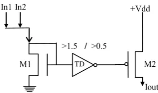
Vdd +
Iout TD
>1.5 / >0.5
M2 M1
In1 In2
Figure 3. Implementation of curent mode double input
AND/OR gates.
TABLE 4. Truth Table of Two Input AND/OR Gates.
Gates Current Output Σin
OR2 AND2
Input Current
OR2 AND2
0 0 0 0 0 0
0.5 0 0 10 μA 0 0
1 1 0 20 μA 20μA 0
2 1 1 40 μA 20μA 20μA Operating with current mode has many advantages
for example the direction of the current can be used to show the sign, eliminating the necessity of using additional bits to show the sign. Another interesting feature in current mode circuits is the ability of creating various circuits by changing only the threshold detector transistors dimensions and sometimes by increasing or decreasing the number of inputs solely. In current mode every bit has its own sign which is an important feature of this mode.
Figure 2, shows the basic circuit for various current mode logic circuits such as: 2-input AND, input AND,…N-input AND, also 2-input OR, 3-input OR,…n-3-input OR and other necessary logic circuits such as majority function.
Iin, can be a factor of the unit current, this
means it can represent the logic two, three, four, etc [1,4,5]. For simplicity,Iincan be broken down into different inputs. e.g. 2 or 3 or … n inputs with unit current instead of one Iin with various currents.
The implementation of AND/OR gates are shown in Figure 3. The algebraic sum of two input currents In1, In2 is done by M1 transistor. The threshold detector unit is shown as an inverter labeled as TD. Changes from high to low happen whenever the algebraic sum of inputs becomes more than the logic 0.5, this activates the PMOS transistor, which results in having an OR gate. An AND gate is achieved if the converter is set to change when the algebraic sum of inputs become the logic 1.5.
Table 4 represents the true table of a two input AND gate as well as a two input OR gate. It is important to observe that none of these two gates respond to logical 0.5 as illustrated in Table 4. This is due to the noise immunity of the circuit which is achieved by applying the exact ratio (W/L) of the pull up to pull down transistors.
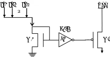
The implementation of Equation 1 which is called the Majority function is shown in Figure 4.
In1In2 + In1In3 + In2In3 (1)
The above capabilities in current mode circuits and the reduction of the number of transistors are very important and crucial in microchip areas and power managements. As can be observed, the uniform structure of these designed circuits, easily
Vdd
TD >1.5
M2 M1
Iout
In1In2In3
Figure 4. Current modeMajority function.
Vdd
TD >0.5
M2 M1
… In1In2 Inn
Figure 5. N-input realization of OR gate.
TABLE 5. Truth Table of N-Input OR.
Σin ORn Input Current CurrentOutput
0 0 0 + Error (0) 0
1 1 20 μA 20 μA
2 1 40 μA 20 μA
3 1 60 μA 20 μA
M M M M
n 1 n*20-Error (n) 20 μA fact no physical change to the circuit in Figure 3 is
needed and in fact the designer can submit the same circuit to the chip manufacturer [1-3].
The actual summation of currents is slightly different with the expected value, and sometimes unexpectedly, from the summation of the two currents of logic 1, logic 2 is not obtained. This error increases as the number of inputs increase, although it causes no error since the OR circuit will change its output condition as soon as it detects the first logic one. In the case of logic zero, fortunately leakage currents are so small that they can be ignored. Table 5 shows the accuracy of the n-input OR circuit. For n > 2 the loss applied by leakage of the algebraic sum of the input increases. As mentioned, the threshold detector changes its output condition as soon as detecting the first logic 1 in its input. The error in logic zero is so small that it does not concede for analysis. The value for the threshold detector has been defined as logic 0.5, which is 10 µA. The error from zero to input 7 that is practically used is less than 1.5 µA. This can be totally ignored.
4. DESIGN OF FULL SWING CURRENT MODE BICMOS CIRCUITS
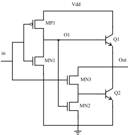
To understand the behavior of the current mode BiCMOS circuits a brief discussion of conventional voltage mode BiCMOS digital circuits makes sense [1]. CMOS technology provides performance superior to NMOS and bipolar technologies in power dissipation, noise margins, packing density and the ability to integrate large complex functions with high yield. As the name “BiCMOS” implies, it is a combination of Bipolar and CMOS technologies. The bipolar technology is used for high switching speed, high driving capability and good noise performance. But CMOS technology ensures low power dissipation, high noise margin and high packing density. Figure 6 shows the conventional BiCMOS inverter.
When input is equal to logical zero, the transistor MP1 is ON and transistors MN1 and MN2 are off, so the Bipolar transistor Q1 is ON. As the voltage at the base of Q1 is equal to logical 1 then MN2 is ON hence, Q2 is off. These facts lead to logical “1” in
output. If the input is equal to logical “1”, all the transistors states will be inverted which results in a logical “0” in the output. Any arbitrary circuit can be implemented using BiCMOS conventional technologies. For example Figure 7 demonstrates an 8-input NAND gate.
O1
Out Vdd
MN2 MN3
Q2 Q1
MN1 MP1
in
Figure 6. Conventional BiCMOS Inverter.
E
A B C D F G H
Out Q1
Q2 E
A B C D F G H
Out Q1
Q2
Figure 7. An 8-input NAND gate.
Vdd
>1.
M1 M3
M5 M4
Iout
In1In2
Figure 8. The circuit diagram of a 2-input XOR gate.
TABLE 6. Truth Table of 2-Input XOR.
Σin XOR2 CurrentInput CurrentOutput
0 0 0 0
1 1 20 µA 20 µA
2 0 40 µA 0
transistors. Using current mode BiCMOS circuits, will show that the number of transistors will not increase, with an increase in the number of inputs.
Figure 8 Shows a 2-input XOR circuit with TD > 1. If the algebraic sum of In1 and In2 is greater than logic 1.5, then the output of the threshold detector changes its state. If the algebraic sum of inputs equals zero, there is no current at the output. If the sum of these inputs is one 1, since the output of TD is high, the M3 transistor is on and input current is copied through current mirror (M1, M2), finally the input current is exactly copied in the output. This means that the logic one at the output will be obtained.
Vdd
TD Vdd
Q1
Q2 M6
M7 P
M2 M1
…
n - Inputs
f Iout = M3
M4
M5
Figure 9. Design of a current mode BiCMOS circuit.
Vdd
M2 …
M3
M5 M4 M1
Q1
Q2
n- Inputs
R2
R1 Vdd
M2 …
M3
M5 M4 M1
Q1
Q2
n- Inputs
R2
R1
Figure 10. The improved BiCMOS circuit.
TABLE 7. Number of Mos Transistors Voltage Mode Verses Proposed Current Mode Bicmos Circuits.
Voltage Mode BiCMOS Current
Mode BiCMOS Technology
Circuit
6 5
2-input NOR
2n + 2 5
n-input NOR
6 5
2-input NAND
2n + 2 5
n-input NAND
14 12
2-input XOR
24 15
n-input XOR
14 11
Improved 3-input XOR Figure 9 shows a design based on BiCMOS
technology. In this circuit the Iout current is applied to transistor M3, through transistor M2. This current, increases the voltage level at point P, as a result transistor M4 switches off and transistor M5, is turned on. This causes M6 to be turned on, and M7 switches off and hence the output of this gate will be logic zero. Also when the Iout current is logic zero, the output will be converted to the logic one.
It should be noted that the delay of this circuit is equal to the sum of delays of one current mode logic gate and a standard inverter BiCMOS.
The advantage of this circuit is its simplicity in design, and the ease for using existing layout for different BiCMOS logics.
5. THE PROPOSED CURRENT MODE BICMOS CIRCUIT
In order to reduce the number of transistors in Figure 9, the TD part of the circuit and one PMOS transistor are eliminated as shown in Figure 10 [1,9]. As mentioned earlier applying a precise ratio of (W/L) pu, to (W/L) pd in a classic CMOS inverter will result in a required TD circuit. This will lead to a considerable increase in overall speed of the circuit.
For full swing operation two resistors R1 and R2 are used for charging and discharging of load capacitance. Without R1 the maximum output voltage will be Vdd-Vbe. Once this voltage reaches Q1 it will turn off. Now, the voltage drop Vbe is compensated by the combination of transistor M2 and resistor R1.
For logic zero, without contribution of R1, R2 and transistor M3, the output will be equal to Vbe of transistor Q2. Whereas after Q2 is turned off using the above combination will result in a further reduction of output to ground potential. The value of R1 and R2 are not very critical as long as they are kept between 0.1 kΩ and a few kilo ohms. The previously mentioned logical circuits can be designed and implemented using the above techniques, resulting in a remarkable reduction of delay in comparison to voltage mode BiCMOS circuits.
TABLE 8. Area Comparison of the Voltage Verses Proposed Current Mode BiCMOS Circuits.
Speedup Percent Voltage Mode
BiCMOS (μm2)
Current Mode BiCMOS (μm2)
Technology
Circuit
% 12 0.779
0.684 2-input NOR
M M
M M
% 100 n→∞
0.513 + 0.133 (n) 0.684
n-input NOR
%10 0.779
0.699 2-input NAND
M M
M M
% 88 n→∞
0.513 + 0.133 (n) 0.668 + 0.016 (n)
n-input NAND
% 50 0.912
0.453 2-input XOR
% 13 1.311
1.13 3-input XOR
Vdd
f
TD
>1.5
M1
Vdd >2.5
TD
f
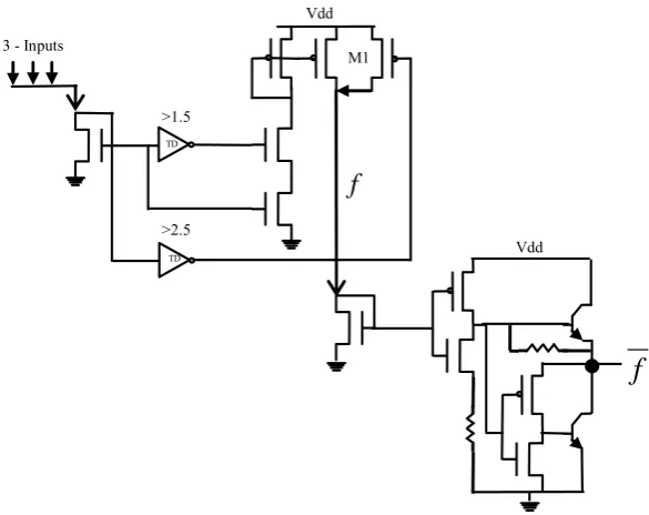
3 - Inputs
Figure 11. Current mode BiCMOS, 3-input XOR.
used in different voltage and current mode BiCMOS circuits.
Table 8, compares the area of different current and voltage mode gates and also the percentage of improvement in speed.
The difference between this circuit and the 2-Figure 11 3 input XOR is that, if the input is higher
than logic 2.5, again a current of logic one is applied to the system by M1 transistor (TD > 1.5). The problem with this circuit is the presence of many current mirrors that slow down the system performance. Table 9 shows the truth table of this circuit.
TABLE 9. Truth Table of the Current Mode BiCMOS, 3-Input XOR Gate.
Input Logic
Input
Current Current f Logic f
0 0 0 1
1 20 μA 20 μA 0
2 40 μA 0 1
3 60 μA 20 μA 0
M3 Vdd TD < ١٫۵ M1 < ٢٫۵ TD M2 Out ٣ - Inputs R2 R1 M3 Vdd TD < ١٫۵ M1 < ٢٫۵ TD M2 Out ٣ - Inputs M3 Vdd TD < ١٫۵ M1 < ٢٫۵ TD M2 Out ٣ - Inputs M3 Vdd TD < ١٫۵ M1 < ٢٫۵ TD M2 Out ٣ - Inputs R2 R1
Figure 12. The improved circuit of 3-inputXOR.
0 1 2 3 4
100 300 500 700 1000 2000
Resistance v ariation of R1 and R2 (Ohm)
Ti m e ( n S )
Fall T ime (ns)
Rise T ime (ns)
Figure 13. Rise and fall time changes versus variation in
resistance R1 and R2.
TABLE 10. Speed Increase in Proposed Current Mode Compared to Voltage Mode.
XOR NAND NOR Circuit Speedup % 6 % 14 % 15 Maximum Speedup % 17 % 13 % 12 Minimum Speedup
XOR Gate using the new logic is shown in Figure 12.
In the above design, two current mirrors and a CMOS inverter gate are eliminated, resulting in a considerable reduction in delay. It should be noted that (W/L) of the M1 transistor is a lot less than (W/L) of M2 transistor, because in the case of ∑ in = 1, the current passing through M2 is equal to a logic 1 (20 µA). But in the case of ∑ in = 3 it is obvious that the maximum current which passes through M2 transistor will be 3 times the logic 1, and this current must be limited in some way. This problem can be eliminated by the decreasing (W/L) of M1 transistor. In actual circuits if voltage mode BiCMOS design is used in a digital system, it is not necessary to decrement this current, since the output voltage is always equal to Vdd-Vbe. Figure 13 shows the effect of variation of resistance values on rise and fall time of the proposed logic circuits. Table 10 compares the speed improvement, in different voltage mode BiCMOS logics with proposed current mode BiCMOS circuits.
The variation of power supply voltage and its effect on rise time and fall time is shown in Figure 14.
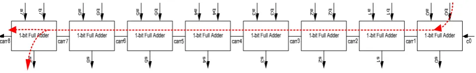
The delay improvement of an 8-bit full adder, as shown in Figure 15 can be compared in voltage and proposed current mode as presented in Table 11.
6. CONCLUSION
0 0.5 1 1.5 2 2.5 3 3.5 4
2.5 3 3.5 5
Voltage (V)
Ti
m
e
(
n
S
)
Rise Time (nS) Fall Time (nS)
Figure 14. Rise and fall time changes versus power supply variation.
Figure 15. Simulated 8-bit ripple adder.
TABLE 11. Simulation Results (8-Bit FA) @ Cload=1pF
Circuit Delay (nm) Improvement %
8-Bit RCA FA, Voltage-Mode 61.3
8-Bit RCA FA, Proposed Circuits 17.0 72
7. REFERENCES
1. Navi, K., Kazemi parsa, M. and Ghorbannia Delavar, A., “Very high speed current mode logical circuits”, The CSI Journal of Computer Science and Engineering, (Spring 2005), 45-50.
2. Chen, C.-L., “2.5 μm BiCMOS Technology”, IEEE
Journal of Solid-State Circuits, Vol. 27, No. 4, (April
1992).
3. Garg, A., Chan Carusone, A. and Voinigescu, S., “A 1-Tap 40-Gbps Look-ahead Decision Feedback Equalizer in 0.18μm SiGe BiCMOS Technology”, IEEE Journal of Solid-State Circuits, (October 2006), 2224-2232.
4. Navi, K., Kazeminejad, A. and Etiemble, D., “Performance of CMOS Current Mode Full Adders”,
IEEE Proc. Int’l. Symp. Multiple Valued Logic, (May
1994), 27-34.
5. Navi, K. and Etiemble, D., “From Multi-Valued Current Mode CMOS Circuits to Efficient Voltage Mode CMOS Arithmetic Operators”, IEEE Proc. Int’l. Symp. Multiple
Valued Logic, (May 1995), 58-64.
6. Arfaee, A. and Navi, K., Kazemi Parsa, M. and Akbari, A., “Design of High Speed 2’s Complement MAC Unit Using Redundant Number System”, 6th Annual Computer Society of Iran Computer Conf., Esfehan,
(2001), 53-58
7. Kazeminejad, A., Navi, K. and Etiemble, D., “CML Current Mode Full Adders for 2.5-V Power Supply”,
IEEE Proc. Int’l. Symp. Multiple Valued Logic, (May
1994), 10-15.
8. Temel, T., Morgül, A., “Implementation of Multi-Valued Logic Gates Using Full Current Mode CMOS Circuits”,
Analog Integrated Circuits and Signal Processing,
KAP, Vol. 39, No. 2, (2004), 191-204.
9. Temel, T., “Current-mode CMOS Design of Multi-Valued Logic Circuits”, PhD Thesis, Bogazici University, Department of Electrical and Electronics Engineering, (2002). 10. Morgul, A. and Turgay, T., “A New Level Restoration