Please cite this article as: N. Binti Mohd Hanib, F.Choong, M. Bin Ibne Reaz, N. Kamal, T. Badal, Bit Swapping Linear Feedback Shift Register For Low Power Application Using 130nm Complementary Metal Oxide Semiconductor Technology, International Journal of Engineering (IJE), TRANSACTIONS B: Applications Vol. 30, No. 8, (August 2017) 1126-1133
International Journal of Engineering
J o u r n a l H o m e p a g e : w w w . i j e . i r
Bit Swapping Linear Feedback Shift Register For Low Power Application Using
130nm Complementary Metal Oxide Semiconductor Technology
N. Binti Mohd Haniba, F.Choong*b, M. Bin Ibne Reaza, N. Kamala, T. Badala
a Department of Electrical, Electronic and Systems Engineering, Universiti Kebangsaan Malaysia, Bangi, Selangor, Malaysia b School of Engineering and Physical Science, Heriot-Watt University, Jalan Venna, Putrajaya, Malaysia.
P A P E R I N F O
Paper history: Received 04 March 2016
Received in revised form 22 May 2017 Accepted 07 July 2017
Keywords:
Bit Swapping Linear Feedback Shift Register Stacking Technique
Low Power
A B S T R A C T
Bit swapping linear feedback shift register (BS-LFSR) is employed in a conventional linear feedback shirt register (LFSR) to reduce its power dissipation and enhance its performance. In this paper, an enhanced BS-LFSR for low power application is proposed. To achieve low power dissipation, the proposed BS-LFSR introduced the stacking technique to reduce leakage current. In addition, three different architectures to enhance the feedback element used in BS-LFSR was explored. The pass transistor merged with transistor stack method yielded a better reduction in power dissipation compared to pass transistor design and NAND gate design. The BS-LFSR was designed in Mentor Graphic – TSMC Design Kit Environment using 130nm complementary metal oxide semiconductor (CMOS) technology. The proposed 4-bit BS-LFSR achieved an active area of 1241.1588um2 and consumed only 53.8844nW with total power savings of 19.43%. The proposed design showed superiority when compared with the conventional LFSR and related work in reducing power dissipation and area.
NOMENCLATURE
𝐶𝐿 Load capacitance
𝐹𝐶𝐿𝐾 Clock frequency
Ileak Leakage current
Pdyn Dynamic power dissipation
𝑉𝐷𝐷 Voltage supply
W Transistor width
𝛼𝑠𝑤 Activity factor (The average switching activity)
1. INTRODUCTION1
The Bit Swapping Linear Feedback Shift Register (BS-LFSR) is introduced to enhance the performance of the basic LFSR. The BS-LFSR design is mainly focusing on reduction of power dissipation by reducing the switching activity in a conventional LFSR without compromising its function and performance. Similar to a conventional LFSR, the BS-LFSR can also produce pseudo-random values in the register due to the feedback element. The selected parameter of BS-LFSR
*Corresponding Author’s Email: [email protected](F.Choong)
such as the seed value, primitive polynomial and tap connection will be able to modify the sequence of the register [1].
BS-LFSR is usually used in Built in Self-Test (BIST) as a test pattern generator (TPG) which requires generating a maximum sequence. BIST method allows an integrated circuit (IC) to perform self-check and test without requiring any extra hardware [2]. This will lead to a reduction in the cost for testing and maintenance of an IC by eliminating the test machine and equipment. Moreover, it can detect any IC failures in a short time interval [3]. Figure 1 shows a basic BIST block diagram including the BS-LFSR circuit as a TPG.
TECHNICAL NOTE
The efficiency of the BS-LFSR depends not only on the parameters such as the seed value, primitive polynomial and tap connection but also can be enhanced by reducing the power dissipation of the LFSR. There has been extensive research carried out to increase the performance and area of very large scale integration (VLSI) design [4-9] and thus improved LFSR design [10-15]. However, some of these work, though give an optimized area and performance, suffers from high power dissipation. Power dissipation is an important consideration in VLSI circuits as it is required to enhance the battery performance and increase the reliability of the VLSI circuit [16]. Hence, a new design focusing on improving the power dissipation is very much needed.
The basic operation of a bit swapping linear feedback shift register (BS-LFSR) is the same as a conventional LFSR. The main characteristic of LFSR as compared to other shift registers is that it can produce a random sequence by choosing a proper feedback function [17]. The period of sequence is (2n-1) for an n bit LFSR with maximum length of 2n-1 long states. The maximum sequence is continuous and once the 2n-1 different values have occurred, it will repeat for the next sequence [18]. A feedback function can be designed by adding an exclusive-OR gate (XOR) on the outputs of the flip – flop (two or more) and feeding the output into the input of the flip – flop, called taps [19, 20]. The extra 2 x 1 multiplexers will be added in a conventional LFSR to reduce the switching activity or number of transitions using bit swapping technique shown in Figure 2 [21, 22].
The basic idea in a BS-LFSR is to move two neighbouring bits on a selected line value of the multiplexer.
Figure 1. BIST block diagram
Figure 2. Bit Swapping LFSR (BS-LFSR)
Consider one of its outputs as selected line and has a specific value of zero (bit n = 0). When n is odd and bit n = 0, bit 1 will be swapped with bit 2, bit 3 with bit 4, and bit n-2 with bit n-1. If n is even and bit n = 0, bit 1 will be swapped with bit 2, bit 3 with bit 4, and bit n-3 with bit n-2. In all cases of the selection line, bit n is excluded from the swapping operation. When bit n = 1, no swapping will be performed. Table 1 shows the comparison of LFSR and BS-LFSR sequence.
As the number of transitions reduce by 4 of the switching activity, it will reduce the dynamic power dissipation in BS-LFSR [11]. The dynamic power dissipation is the primary source of the power dissipation in CMOS circuits. During switching activity, the power is dissipated due to the short circuit current and also the charging of load capacitances as given in Equation (1) [22, 23];
𝑃𝑑𝑦𝑛= 12𝑉𝐷𝐷2 𝛼𝑠𝑤𝐶𝐿𝐹𝐶𝐿𝐾 (1)
where; 𝑉𝐷𝐷 = Voltage supply, 𝛼𝑠𝑤 = Activity
factor (The average switching activity), 𝐶𝐿 = The load
capacitance , 𝐹𝐶𝐿𝐾 = The clock frequency.
Based on Equation (1), the dynamic power can be influenced by three parameters including the voltage supply, the clock frequency and an activity factor or switching activity.
TABLE 1. The comparison of LFSR and BS-LFSR sequence
[5]
LFSR output BS-LFSR output
1 0 1 0 0 1 1 0
0 1 0 1 0 1 0 1
1 0 1 1 1 0 1 1
0 1 1 1 0 1 1 1
1 1 1 1 1 1 1 1
1 1 1 0 1 1 1 0
1 1 0 0 1 1 0 0
1 0 0 0 0 1 0 0
0 0 0 1 0 0 0 1
0 0 1 0 0 0 1 0
0 1 0 0 1 0 0 0
1 0 0 1 1 0 0 1
0 0 1 1 0 0 1 1
0 1 1 0 1 0 1 0
1 1 0 1 1 1 0 1
1 0 1 0 0 1 1 0
No of transitions
8 8 8 8 8 4 8 8
Total no. of transitions
However, changing the power supply and clock frequency to decrease the dynamic power dissipation will decrease the efficiency of the circuit. In contrast, reducing the switching activity will not decrease the performance of the circuit [24].
This work introduces an enhanced BS-LFSR for low power application by applying the stacking technique to reduce leakage current. In addition, three different architectures to enhance the feedback element used in BS-LFSR is explored. The number of transistors, power dissipation and layout area of LFSR is varied in different architectures. In addition, design enhancements such as transistor reverse body bias (RBB) and stack implemented on the gate is presented. The improved design can be merged with other low power techniques for future development in low power dissipation.
The organization of the paper is as follows. Firstly, the overview of BS-LFSR including the working principles are discussed. Next, the proposed design to reduce the power dissipation in BS-LFSR is presented. This is followed by presentation of results and discussion along with the comparison with related work. The paper concludes with a summary and future work.
2. METHODOLOGY
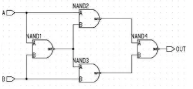
This section will introduce the design of the BS-LFSR incorporating the stacking technique and several enhancements to the feedback element. Figure 3 shows the design of XOR gate using NAND gate architecture. Four units of NAND gates are used to design the XOR gate involving a total of 16 transistors. The use of NAND gate will eliminate the problems of contention and race in the circuit [25]. However, this design consumes a large area due to high number of transistors used and also suffers from high power dissipation. In contrast, pass transistor architecture is able to reduce the number of transistors needed by reducing the number of gates.
This is achieved by removing the switches that are connected to the supply. However, if all the transistors have the same threshold voltage, then the node voltage at the end of the pass transistor will become lower than VDD [26].
Figure 3. The XOR gate design using NAND gate
architecture
To overcome this problem, the reverse bias body method can be applied by raising the threshold voltage during standby mode [27]. By applying reverse bias to the body of the transistor, the threshold voltage can be adjusted due to the body effect. For example, biasing an NMOS body with ground, or biasing a PMOS body with VDD will increase the threshold voltage. Figure 4 shows the feedback element designed using pass transistor architecture involving only six transistors.
In order to further reduce the power dissipation, transistor stacking method can be applied to the pass transistor design [26, 28]. This will reduce the leakage currents hence reduce the static power dissipation. The leakage current flowing through a stack of transistors connected in series reduces when more than one transistor of the stack is turned OFF, known as the stacking effect [26]. When two or more transistors that are switched OFF are stacked on top of each other they dissipate less leakage power than a single transistor that is turned OFF as shown in Figure 5 and described by Equation (2).
Ileak1 < Ileak2 (2)
where; Ileak1 = IleakT1 + IleakT2 + IleakT3, IleakT1 > IleakT2 > IleakT3
Figure 6 shows the stacking effect of a single transistor of width W is being replaced by two transistors each of width W/2.
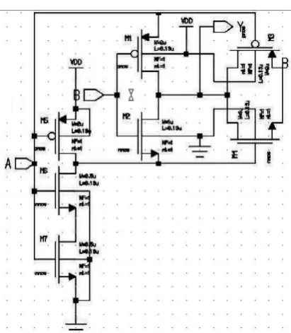
In the proposed design, the enhanced feedback element using pass transistors and stacking technique is shown in Figure 7. An additional transistor is used in this circuit (M7) for creating the stacking effect. The total size of M6 and M7 is equivalent to M6 in Figure 6. Therefore, the leakage current that flows through M6 is higher as compared to the leakage current flowing through M6 in Figure 7.
Figure 4. The XOR gate design using pass transistor
Figure 5. Transistor stack effect
Figure 6. Transistor stack effect arrangement
Figure 7. Feedback element (XOR gate) improved using
stacking technique
3. RESULTS AND DISCUSSION
The proposed architecture is designed using Mentor Graphic TSMS Design Kit Environment. CEDEC_KIT is an ASIC Design Kit for Mentor Graphic design tools.
It is used to prepare the BS-LFSR to be fabricated based on TSMC 0.13 micron technology. The proposed BS-LFSR circuit performance is verified using Eldo RF simulator of Mentor Graphic and transistor process parameters in accordance to Collaborative Micro-electronic Design Excellence Centre (CEDEC) 0.13um standard CMOS process.
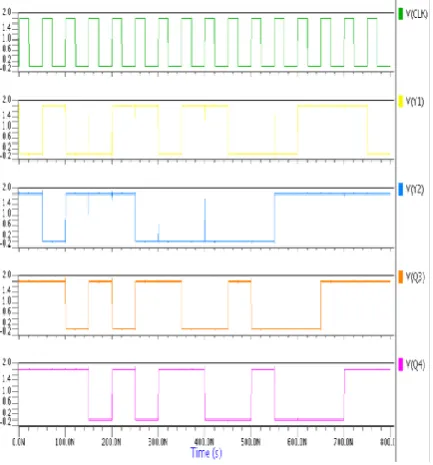
All the simulation results presented are based on the 4 bit BS-LFSR as shown in Figure 8. The seed value for this circuit has been set as ‘1111’ and VDD set at 1.8v. The feedback element used in this circuit can be derived using a characteristic polynomial f(x) = 1 + x + x4. The maximum sequence of 4-bit LFSR is (24 – 1) = 15 and the taps (feedback function) are Q1 and Q4. Figure 9(a) and Figure 9(b) show the output waveform for the conventional LFSR and the proposed BS-LFSR respectively.
The transition between LFSR and BS-LFSR has been compared and presented in Table 2. The comparison is based on the transition occurred in the output waveform of LFSR.
The proposed design reduced the transition activity by 12.5% and power dissipation by 8.3589 nW. The results correlates to Equation (1) whereby reducing the transition activity will reduce the power dissipation of the circuit. Based on the comparison, it can be concluded that the swapping technique can reduce the transition activity hence reducing the power dissipation.
In addition to the swapping technique, the proposed design also considered three different architectures for the feedback element as shown in Table 3. The performance of the BS-LFSR can be evaluated through certain parameters by looking at the various architectures of XOR gate. The number of transistors, power dissipation and layout area of the XOR gate are varied in different architectures.
Figure 9(a). Output waveform of conventional LFSR
Figure 9(b). Output waveform of BS-LFSR
Based on Table 3, it is noticed that the power dissipation is much lower if pass transistor is used as compared to NAND gate with a reduction of 32.17%. The same trend is also seen in the number of transistor and layout area. The area is reduced to half from the NAND gate design. It is also seen that the transistor stack method on pass transistor yielded more reduction in power dissipation as low as 2.7053 nW.
TABLE 2. The comparison between LFSR and the proposed
BS-LFSR
LFSR output (Figure 9a) BS-LFSR output (Figure 9b)
Q1 Q2 Q3 Q4 Y1 Y2 Q3 Q4
1 1 1 1 1 1 1 1
0 1 1 1 0 1 1 1
1 0 1 1 1 0 1 1
0 1 0 1 0 1 0 1
1 0 1 0 0 1 1 0
1 1 0 1 1 1 0 1
0 1 1 0 1 0 1 0
0 0 1 1 0 0 1 1
1 0 0 1 1 0 0 1
0 1 0 0 1 0 0 0
0 0 1 0 0 0 1 0
0 0 0 1 0 0 0 1
1 0 0 0 0 1 0 0
1 1 0 0 1 1 0 0
1 1 1 0 1 1 1 0
1 1 1 1 1 1 1 1
No of transition
8 8 8 8 8 4 8 8
Total no. of transition
32 28
Power dissipation
66.875 nW 58.5167 nW
TABLE 3. The comparison of different architecture in design
of XOR Gate
Performance NAND
Gate
Pass Transistor (PT)
PT + Staking Method
No of transistor 16 6 7
Current (nA) 3.1023 2.1043 1.503
Power dissipation (nW) 5.5842 3.7877 2.7053
% Saving - 32.17% 51.55%
Layout area (um)2 71.5343 35.3509 47.5405
% Saving - 50.58% 33.54%
However, there is a slight increase in the area as compared to the pass transistor design.
pass transistor design and NAND gate design. This method reduced the power dissipation to around 53.8844 nw, a 7.99% reduction as compared to BS-LFSR using NAND gate design. In conclusion, in order to optimize the LFSR for power, the better design will be the BS-LFSR incorporating pass transistor and stacking method. It will reduce the power dissipation as well as reduce the current.
Finally, the proposed design was compared with previous work on BS-LFSR as shown in Table 5.
TABLE 4. The comparison of XOR gate design implemented
in BS-LFSR
Performance NAND
Gate
Pass Transistor
(PT)
PT + Staking Method
Current (nA) 32.5093 30.0211 29.9358
Power dissipation (nW) 58.5167 54.0379 53.8844
% Saving - 7.65% 7.99%
Layout area (um)2 1356.992 1234.32 1241.1588
% Saving - 9.04% 8.54%
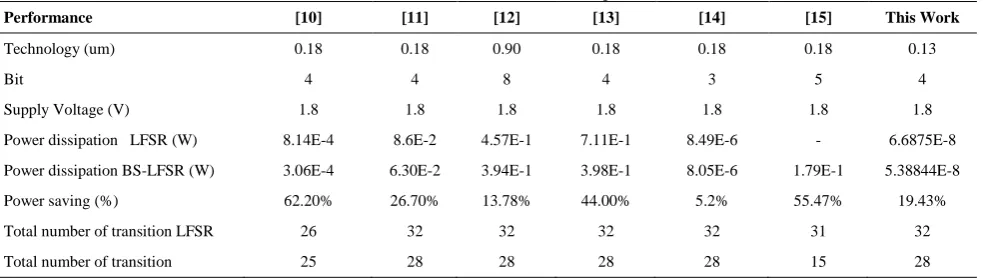
TABLE 5. BS-LFSR Performance Comparison
Performance [10] [11] [12] [13] [14] [15] This Work
Technology (um) 0.18 0.18 0.90 0.18 0.18 0.18 0.13
Bit 4 4 8 4 3 5 4
Supply Voltage (V) 1.8 1.8 1.8 1.8 1.8 1.8 1.8
Power dissipation LFSR (W) 8.14E-4 8.6E-2 4.57E-1 7.11E-1 8.49E-6 - 6.6875E-8
Power dissipation BS-LFSR (W) 3.06E-4 6.30E-2 3.94E-1 3.98E-1 8.05E-6 1.79E-1 5.38844E-8
Power saving (%) 62.20% 26.70% 13.78% 44.00% 5.2% 55.47% 19.43%
Total number of transition LFSR 26 32 32 32 32 31 32
Total number of transition 25 28 28 28 28 15 28
It is seen that the design in literature [10] provides a much lower power dissipation by implementing an additional of two XOR gates and one NOR gate as a feedback element. However, this increased the number of transistors and layout area. Also, the design only managed to reduce the switching activity by one transition. The work in reference [15] introduced a single inverter to control a clock at each D flip flop (DFF) and also used four multiplexers to control the output from DFF. This managed to further reduce the transition activity to 16 transitions. However, the drawback of this design is high power dissipation and larger area due to the increased number of transistors. It is also seen that implementing a smaller CMOS technology does not necessarily lead to a lower power dissipation. In reference [12], the design employed a 90nm and 8 bit BS-LFSR. It can be concluded that the proposed BS-LFSR managed to obtain amongst the lower power dissipation by implementing the stacking method. For the overall design, the number of transitions can only reduce to 4 steps by introducing multiplexer element.
4. CONCLUSION
The bit swapping linear feedback shift register (BS-LFSR) using pass transistor and stacking method for low power application using 130nm CMOS technology
is proposed. It has an active area of 1241.1588um2 and consumed only 53.8844nW with total power savings of 19.43%. The proposed design showed superiority when compared with the conventional LFSR and related work in reducing power dissipation and area. Future work will involve combining the proposed design with other power reduction techniques to further optimize its performance.
5. REFERENCES
1. Nyathi, J., Delgado-Frias, J.G. and Lowe, J., "A high performance, hybrid wave-pipelined linear feedback shift register with skew tolerant clocks", in Circuits and Systems, IEEE 46th Midwest Symposium on,. Vol. 3, (2003), 1384-1387. 2. S, S. and M, T., "A low power structure design of 2d-lfsr and
encoding technique for bist", International Journal of Advanced Science and Technology, Vol. 18, (2010), 11-22. 3. Dufaza, C., "Theoretical properties of lfsrs for built-in self test",
Integration, the VLSI Journal, Vol. 25, No. 1, (1998), 17-35. 4. Chae, Y. and Han, G., "Low voltage, low power, inverter-based
switched-capacitor delta-sigma modulator", IEEE Journal of Solid-State Circuits, Vol. 44, No. 2, (2009), 458-472. 5. Fallah, M. and MiarNaimi, H., "A novel low voltage, low power
and high gain operational amplifier using negative resistance and self cascode transistors", International Journal of Engineering-Transactions C: Aspects, Vol. 26, No. 3, (2012), 303-310. 6. Kebbati, Y., "Modular approach for an asic integration of
Engineering-Transactions B: Applications, Vol. 24, No. 2, (2011), 107-115.
7. Teh, Y.-K., Mohd-Yasin, F., Choong, F., Reaz, M.I. and Kordesch, A.V., "Design and analysis of uhf micropower cmos dtmost rectifiers", IEEE Transactions on Circuits and Systems II: Express Briefs, Vol. 56, No. 2, (2009), 122-126.
8. Farshidi, E. and Keramatzadeh, A., "A new approach for low voltage cmos based on current-controlled conveyors",
International Journal of Engineering, Vol. 27, No. 5, (2014), 723-730.
9. Mohd-Yasin, F., Teh, Y., Choong, F. and Reaz, M., Two cmos bgr using cm and dtmost techniques. (2009), Abdus Salam International Centre for Theoretical Physics.
10. Kamath, H.S., Nath, A., Srivastava, S.K. and Garg, S., "Comparative power analysis of lfsr test pattern generators",
International Journal of Computer Applications, Vol. 98, No. 8, (2014).
11. Reddy, C.R.S. and Sumalatha, V., "A new built in self test pattern generator for low power dissipation and high fault coverage", in Intelligent Computational Systems (RAICS), IEEE Recent Advances in,. (2013), 19-25.
12. Banupriya, C. and Chandrakala, S., "A low power built in repair analyzer for word oriented memories with optimal repair rate", in Green Computing Communication and Electrical Engineering (ICGCCEE), International Conference on, IEEE., (2014), 1-5. 13. Prasanna, G.D., Abinaya, P. and Poornimasre, J., "Non-intrusive
bit swapping pattern generator for bist testing of luts", in Information Communication and Embedded Systems (ICICES), International Conference on, IEEE., (2014), 1-4.
14. Praveen, J. and Shanmukhaswamy, M.N., "Power reduction technique in lfsr using modified control logic for vlsi circuit", International Journal of Computer Applications, No. 4, (2013), 21-24.
15. Krishna, K.M. and Sailaja, M., "Low power memory built in self test address generator using clock controlled linear feedback shift registers", Journal of Electronic Testing, Vol. 30, No. 1, (2014), 77-85.
16. Kaur, K. and Noor, A., "Strategies & methodologies for low power vlsi designs: A review", International J. Advances in Engineering & Technology, Vol. 1, (2011), 159-165.
17. Li, C., Zeng, X., Helleseth, T., Li, C. and Hu, L., "The properties of a class of linear fsrs and their applications to the construction of nonlinear fsrs", IEEE Transactions on Information Theory, Vol. 60, No. 5, (2014), 3052-3061.
18. Marufuzzaman, M., Rosly, H.N.B., Reaz, M.B.I., Rahman, L.F. and Hussain, H., "Design of low power linear feedback shift",
Journal of Theoretical & Applied Information Technology, Vol. 61, No. 2, (2014), 326-333.
19. Sowmiya, G., Premalatha, P., Rajaram, A., Saravanan, S. and Sai, R.V., "Design and analysis of scan power reduction based on linear feedback shift register reseeding", in Information & Communication Technologies (ICT), IEEE Conference on, IEEE., (2013), 638-641.
20. Ahmad, A. and Al-Maashri, A., "Investigating some special sequence lengths generated in an external exclusive-nor type LFSR", Computers & Electrical Engineering, Vol. 34, No. 4, (2008), 270-280.
21. Saraswathi, T., Ragini, K. and Ch, G.R., "A review on power optimization of linear feedback shift register (lfsr) for low power built in self test (BIST)", in Electronics Computer Technology (ICECT), 3rd International Conference on, Vol. 6, (2011), 172-176.
22. Kavitha, A., Seetharaman, G., Prabakar, T. and Shrinithi, S., "Design of low power tpg using lp-lfsr", in Intelligent Systems, Modelling and Simulation (ISMS), Third International Conference on, IEEE., (2012), 334-338.
23. Muthammal, R. and Joseph, K., "Low power efficient built in self test", in Microwaves, Communications, Antennas and Electronics Systems (COMCAS), International Conference on, IEEE., (2011), 1-5.
24. Zadeh, A.A. and Heys, H.M., "Simple power analysis applied to nonlinear feedback shift registers", IET Information Security, Vol. 8, No. 3, (2014), 188-198.
25. Rebaud, B., Belleville, M., Bernard, C., Robert, M., Maurine, P. and Azemard, N., "A comparative study of variability impact on static flip-flop timing characteristics", in Integrated Circuit Design and Technology and Tutorial,. ICICDT. IEEE International Conference on,.(2008), 167-170.
26. Sheela, T., Muthumanickam, T. and Nagappan, A., "A lfsr based binary numeral system using cmos vlsi", International Journal of VLSI and Embedded Systems-IJVES ISSN, No. 2249-6556. 27. Rani, M.J. and Malarkkan, S., "Design and analysis of a linear feedback shift register with reduced leakage power",
International Journal of Computer Applications, Vol. 56, No. 14, (2012).
Bit Swapping Linear Feedback Shift Register For Low Power
Application Using 130nm Complementary Metal Oxide Semiconductor
Technology
TECHNICAL NOTE
N. Binti Mohd Haniba, F.Choongb, M. Bin Ibne Reaza, N. Kamala, T. Badala
a Department of Electrical, Electronic and Systems Engineering, Universiti Kebangsaan Malaysia, Bangi, Selangor, Malaysia b School of Engineering and Physical Science, Heriot-Watt University, Jalan Venna, Putrajaya, Malaysia.
P A P E R I N F O
Paper history: Received 04 March 2016
Received in revised form 22 May 2017 Accepted 07 July 2017
Keywords:
Bit Swapping Linear Feedback Shift Register Stacking Technique
Low Power
ديكچ ه
تيب یياجباج تروص هب یطخ کبديف اب رتسيجر تفيش (Bit Swapping)
BS-LFSR اب رتسيجر تفيش کي رد
ديف
دهد شهاک ار نآ ناوت تافلت ات تسا هدش هتفرگ راکب فراعتم یطخ کب آ درکراک و
کي هلاقم نيا رد .دشخب دوبهب ار ن
BS-LFSR ،نيياپ تافلت هب نتفاي تسد یارب .تسا هدش داهنشيپ نيياپ ناوتدربراکروظنم هب هتفاي دوبهب
BS-LFSR هئارا
شور هدش stacking دنک یم یفرعم ار .دهد شهاک ار یتشن نايرج ات
روتسيزنارت ماغدا pass
روتسيزنارت شوراب stack
تسيزنارت حرط اب هسياقم رد ار یرتهب هدش فلت ناوت شهاک رو
pass تيگ حرط و NAND
.تسا هداد تسدب
BS-LFSR یحارط تيک طيحم رد Mentor Graphic-TSMC
یروانف زا هدافتسا اب nm CMOS
130 هتفرگ تروص
.تسا BS-LFSR لاعف تحاسم هب یداهنشيپ یتيبراهچ
µm2
15 / 1241 طقف و هديسر nW
8844 / 53 و یيوج هفرص
ناوت لداعم ی 43 / 19 % تسا هدرک فرصم .
حرط یداهنشيپ اب هسياقم رد LFSR
فراعتم شهاک رظن زا طوبرم درکراک و
![TABLE 1.[5]](https://thumb-us.123doks.com/thumbv2/123dok_us/206230.2014940/2.595.308.542.457.758/table.webp)