University of Pennsylvania
ScholarlyCommons
Publicly Accessible Penn Dissertations
1-1-2016
Energy Reduction Through Voltage Scaling and
Lightweight Checking
Edin Kadric
University of Pennsylvania, ekadric@seas.upenn.edu
Follow this and additional works at:http://repository.upenn.edu/edissertations
Part of theComputer Engineering Commons, and theElectrical and Electronics Commons
Recommended Citation
Kadric, Edin, "Energy Reduction Through Voltage Scaling and Lightweight Checking" (2016).Publicly Accessible Penn Dissertations. 1794.
Energy Reduction Through Voltage Scaling and Lightweight Checking
Abstract
As the semiconductor roadmap reaches smaller feature sizes and the end of Dennard Scaling, design goals change, and managing the power envelope often dominates delay minimization. Voltage scaling remains a powerful tool to reduce energy. We find that it results in about 60% geomean energy reduction on top of other common low-energy optimizations with 22nm CMOS technology. However, when voltage is reduced, it becomes easier for noise and particle strikes to upset a node, potentially causing Silent Data Corruption (SDC). The 60% energy reduction, therefore, comes with a significant drop in reliability. Duplication with checking and triple-modular redundancy are traditional approaches used to combat transient errors, but spending 2–3x the energy for redundant computation can diminish or reverse the benefits of voltage scaling. As an alternative, we explore the opportunity to use checking operations that are cheaper than the base computation they are guarding. We devise a classification system for applications and their lightweight checking characteristics. In particular, we identify and evaluate the effectiveness of lightweight checks in a broad set of common tasks in scientific computing and signal processing. We find that the lightweight checks cost only a fraction of the base computation (0-25%) and allow us to recover the reliability losses from voltage scaling. Overall, we show about 50% net energy reduction without compromising reliability compared to operation at the nominal voltage. We use FPGAs (Field-Programmable Gate Arrays) in our work, although the same ideas can be applied to different systems. On top of voltage scaling, we explore other common low-energy techniques for FPGAs: transmission gates, gate boosting, power gating, low-leakage (high-Vth) processes, and dual-V dd architectures.
We do not scale voltage for memories, so lower voltages help us reduce logic and interconnect energy, but not memory energy. At lower voltages, memories become dominant, and we get diminishing returns from continuing to scale voltage. To ensure that memories do not become a bottleneck, we also design an energy-robust FPGA memory architecture, which attempts to minimize communication energy due to mismatches between application and architecture. We do this alongside application parallelism tuning. We show our techniques on a wide range of applications, including a large real-time system used for Wide-Area Motion Imaging (WAMI).
Degree Type Dissertation
Degree Name
Doctor of Philosophy (PhD)
Graduate Group
Electrical & Systems Engineering
First Advisor Andre DeHon
Keywords
Communication, Energy, FPGA, Lightweight Check, Memory, Power
Subject Categories
ENERGY REDUCTION THROUGH VOLTAGE
SCALING AND LIGHTWEIGHT CHECKING
Edin Kadric
A DISSERTATION
in Electrical and Systems Engineering
Presented to the Faculties of the University of Pennsylvania in Partial Fulfillment of the Requirements for the
Degree of Doctor of Philosophy 2016
Supervisor of Dissertation Signature
Andr´e DeHon, Professor of Electrical and Systems Engineering
Graduate Group Chair Signature
Alejandro Ribeiro, Rosenbluth Associate Professor of Electrical and Systems Engineering
Dissertation Committee:
Andr´e DeHon, Professor of Electrical and Systems Engineering Randy Huang, Intel
ENERGY REDUCTION THROUGH VOLTAGE SCALING
AND LIGHTWEIGHT CHECKING
COPYRIGHT
2016
Acknowledgements
I would like to thank Andr´e DeHon for so many things. I have been very fortunate
to get to know him and work with him over the last few years. His expertise, insight
and dedication have guided this work in the best of ways. He also contributed to
much of the written content. He is the best advisor and mentor I could have asked
for.
I would like to thank the members of my defense committee: Randy Huang,
Jonathan M. Smith, and Jan Van der Spiegel. Their advice and feedback have greatly
helped strengthen this dissertation.
I would like to thank the members of the IC lab, who have contributed to shaping
this work through discussion and feedback. In particular, Udit Dhawan, Benjamin
Gojman, and Rafi Rubin, who have taught me many important tricks, shared ideas,
and provided much technical help and tool support.
I would also like to thank my parents and my brother for the invaluable support
and encouragement they have always provided me.
Finally, I would like to thank my wife and best friend Emina. Her constant love,
ABSTRACT
ENERGY REDUCTION THROUGH VOLTAGE SCALING
AND LIGHTWEIGHT CHECKING
Edin Kadric
Andr´e DeHon
As the semiconductor roadmap reaches smaller feature sizes and the end of
Den-nard Scaling, design goals change, and managing the power envelope often dominates
delay minimization. Voltage scaling remains a powerful tool to reduce energy. We
find that it results in about 60% geomean energy reduction on top of other common
low-energy optimizations with 22 nm CMOS technology. However, when voltage is
reduced, it becomes easier for noise and particle strikes to upset a node, potentially
causing Silent Data Corruption (SDC). The 60% energy reduction, therefore, comes
with a significant drop in reliability. Duplication with checking and triple-modular
redundancy are traditional approaches used to combat transient errors, but spending
2–3× the energy for redundant computation can diminish or reverse the benefits of voltage scaling. As an alternative, we explore the opportunity to use checking
oper-ations that are cheaper than the base computation they are guarding. We devise a
classification system for applications and their lightweight checking characteristics. In
particular, we identify and evaluate the effectiveness of lightweight checks in a broad
set of common tasks in scientific computing and signal processing. We find that the
us to recover the reliability losses from voltage scaling. Overall, we show about 50%
net energy reduction without compromising reliability compared to operation at the
nominal voltage. We use FPGAs (Field-Programmable Gate Arrays) in our work,
al-though the same ideas can be applied to different systems. On top of voltage scaling,
we explore other common low-energy techniques for FPGAs: transmission gates, gate
boosting, power gating, low-leakage (high-Vth) processes, and dual-Vdd architectures.
We do not scale voltage for memories, so lower voltages help us reduce logic and
interconnect energy, but not memory energy. At lower voltages, memories become
dominant, and we get diminishing returns from continuing to scale voltage. To
en-sure that memories do not become a bottleneck, we also design an energy-robust
FPGA memory architecture, which attempts to minimize communication energy due
to mismatches between application and architecture. We do this alongside
applica-tion parallelism tuning. We show our techniques on a wide range of applicaapplica-tions,
Contents
Acknowledgements iii
Abstract iv
List of Tables xiii
List of Figures xvi
1 Introduction 1
1.1 Thesis . . . 1
1.2 Motivation . . . 1
1.3 Outline . . . 3
1.4 Common low-energy optimizations (Chapter 3) . . . 4
1.5 Parallelism and communication energy (Chapter 4) . . . 7
1.6 Maintaining reliability using LWCs (Chapters 5 and 6) . . . 9
1.7 WAMI case study (Chapter 7) . . . 10
1.8 Contributions and scope . . . 11
1.9 Publications . . . 13
2 Background 14 2.1 FPGA models . . . 14
2.1.1 FPGA architecture . . . 14
2.1.3 Benchmarks . . . 18
2.1.4 FPGA energy modeling . . . 20
2.1.5 FPGA memory energy . . . 20
2.2 Previous work on energy optimizations . . . 21
2.2.1 Technology scaling . . . 21
2.2.2 Transmission gates, gate boosting . . . 22
2.2.3 Power gating . . . 23
2.2.4 Multiple supply voltages . . . 23
2.2.4.1 Lower voltage off the critical path . . . 23
2.2.4.2 Differential reliability . . . 24
2.3 Previous work on lightweight checking . . . 25
2.4 Previous work on reliability . . . 26
2.4.1 Upset phenomena and voltage scaling . . . 26
2.4.2 Prior work on soft-error upsets and timing failures . . . 27
2.4.3 Configuration upsets . . . 27
2.4.4 Process variation . . . 28
2.4.5 Aging . . . 29
3 Common Low-Energy Optimization Techniques 30 3.1 Introduction . . . 30
3.2 Architecture and benchmarks . . . 31
3.3 Simple voltage scaling . . . 32
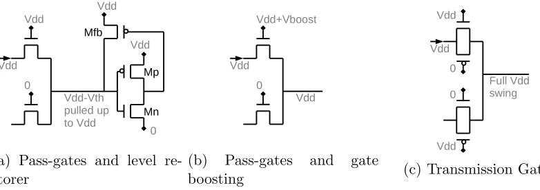
3.4 Transmission gates or gate boosting . . . 33
3.4.1 Pass-transistor and level restorer failure . . . 33
3.4.2 Transmission gate, gate boosting results . . . 35
3.4.3 Technology trends . . . 39
3.5 Power gating . . . 40
3.5.1 Power switches for power gating . . . 40
3.6 Dual-Vdd architectures . . . 44
3.6.1 Motivation and approach . . . 44
3.6.2 Power switches for dual-Vdd . . . 45
3.6.3 Level converters for dual-Vdd . . . 46
3.6.4 Vdd assignment algorithm . . . 47
3.6.5 Dual-Vdd results . . . 48
3.7 Discussion . . . 50
3.7.1 Relative benefits . . . 50
3.7.2 Results spread . . . 51
4 Communication Energy: Adjusting Parallelism and Memory Orga-nization 54 4.1 Introduction . . . 54
4.2 Parallelism and data movement energy . . . 55
4.2.1 Memory energy . . . 56
4.2.2 Between computations . . . 57
4.2.3 Analysis . . . 58
4.3 Architecture mismatch energy . . . 61
4.4 Background on FPGA memories . . . 68
4.4.1 FPGA memory architecture . . . 68
4.4.2 Memory energy modeling . . . 69
4.5 Methodology for memory exploration . . . 70
4.5.1 Power-optimized memory mapping . . . 71
4.5.2 Energy and area of memory blocks . . . 72
4.5.3 Benchmarks . . . 73
4.5.4 Limit study and mismatch lower bound . . . 77
4.6 Parallelism tuning . . . 78
4.6.1 Example: MMul . . . 78
4.6.3 Parallelism tuning with concrete FPGA architecture . . . 79
4.7 Memory exploration . . . 81
4.7.1 Memory block size sweep . . . 81
4.7.2 Impact of dm . . . 83
4.7.3 Impact of memory width . . . 85
4.7.4 Sensitivity . . . 85
4.8 Chapter conclusions . . . 86
5 Lightweight Checking Classification 89 5.1 Introduction . . . 89
5.2 Computational model . . . 89
5.3 Differential reliability . . . 90
5.4 LWC definition . . . 91
5.5 Classification system for LWCs . . . 93
5.6 Class #1: Checksums . . . 95
5.6.1 LWC for sorting . . . 97
5.6.2 LWC for matrix multiplication . . . 98
5.6.3 LWC for FFT . . . 101
5.6.4 LWC Gaussian elimination . . . 102
5.6.5 LWC for window filtering . . . 103
5.6.6 LWC for integer multiplication, division, modulo . . . 104
5.6.7 LWC for data integrity . . . 105
5.7 Class #2: Probabilistic . . . 105
5.7.1 Probabilistic LWC for matrix multiplication . . . 106
5.7.2 Probabilistic LWC for matrix inversion . . . 106
5.8 Class #3: Convergent algorithms . . . 107
5.8.1 LWC for conjugate gradient . . . 108
5.9 Class #5: Error-tolerant applications . . . 109
5.11 Using context . . . 112
5.12 Impact of communication complexity . . . 113
5.13 Combining different LWCs . . . 113
5.14 Chapter conclusions . . . 114
6 Lightweight Checking Models and Results 115 6.1 Introduction . . . 115
6.2 Reliability models . . . 116
6.2.1 Energy savings analysis . . . 116
6.2.2 Silent data corruption (SDC) rate . . . 118
6.2.3 Fault injection runtime . . . 123
6.2.4 Bit flip rate versus voltage . . . 123
6.3 Lightweight checking results . . . 126
6.3.1 Detailed LWC example: sorting . . . 127
6.3.1.1 Impact on energy when considering reliability . . . . 127
6.3.1.2 Analysis . . . 128
6.3.1.3 Parameter sweep . . . 130
6.3.1.4 Effect of problem size on LWC results . . . 131
6.3.2 LWC results for the other applications . . . 132
6.3.2.1 Basic LWC results for all benchmarks . . . 132
6.3.2.2 Improving delay . . . 134
6.3.2.3 Sensitivity analysis . . . 136
6.3.2.4 Fault injection results . . . 138
6.4 Discussion . . . 139
7 Full System Case Study: WAMI 140 7.1 Introduction . . . 140
7.2 Top level: Wide-Area Motion Imaging, WAMI . . . 141
7.3.1 Bayer filtering . . . 141
7.3.2 LWC for DeBayer . . . 142
7.4 Stage 2: Lucas-Kanade . . . 145
7.4.1 LK algorithm . . . 145
7.4.2 LK implementation in hardware . . . 148
7.4.2.1 Fixed-point arithmetic . . . 148
7.4.2.2 Parallel LK . . . 149
7.4.2.3 Caching scheme for the warp . . . 150
7.4.2.4 Structure of LK in hardware . . . 152
7.4.3 LWC for LK . . . 154
7.5 Stage 3: Gaussian Mixture Modeling . . . 157
7.5.1 GMM overview . . . 157
7.5.2 GMM implementation . . . 158
7.5.3 LWC for GMM . . . 159
7.6 WAMI results . . . 159
7.6.1 Basic WAMI results . . . 159
7.6.2 Parallelism benefits . . . 160
7.6.3 Other metrics . . . 161
7.7 Chapter conclusions . . . 163
8 Future Work 164 8.1 Technology . . . 164
8.2 Automation . . . 165
8.3 Reliability . . . 165
8.3.1 Error modeling . . . 165
8.3.2 Variation . . . 166
8.3.3 Fault injection simulation . . . 167
8.3.4 Limits on larger applications . . . 167
8.4 Architecture . . . 168
8.4.1 FPGA structure . . . 168
8.4.2 Multi-Vdd . . . 169
8.4.3 Joint exploration of memory architecture and voltage scaling . 169
9 Conclusions 170
Appendices 172
A Detailed Results for Chapter 3 173
List of Tables
2.1 Taxonomy of small-feature-size reliability problems . . . 26
4.1 Memory requirements for the benchmarks . . . 74
4.2 Area comparison of select memory organizations . . . 85
5.1 LWC classes and example applications (problems with P complexity) . 96
6.1 Possible outcomes of the protected design (CMP+LWC) . . . 121
6.2 Fault injection results for Sort (N = 1024, P = 1) . . . 127
6.3 Ratio results for CMP-only single-Vdd normalized to “CMP at Vnominal” 134
6.4 Ratio results for CMP+LWC single-Vddnormalized to “CMP atVnominal”
(Tab. 6.3 baseline) . . . 134
6.5 Ratio results for CMP+LWC dual-Vdd normalized to “CMP atVnominal”
(Tab. 6.3 baseline) . . . 135
6.6 LWC fault injection results (no bit flip in LWC) . . . 139
List of Figures
1.1 Effect of voltage scaling on energy, delay, and reliability; example from
Sec. 6.3.1.1 with HP (High-Performance) process . . . 3
1.2 Resulting energy when applying the different low-energy techniques, nor-malized to a 22 nm HP baseline at nominal Vdd with pass-gates and no power gating . . . 6
2.1 Basic FPGA model used for logic and routing . . . 15
2.2 Tool flow . . . 19
3.1 Effect of voltage scaling on energy and delay for the baseline architecture (ignoring pass-gate failures) . . . 33
3.2 Pass-gate versus transmission gate 2-mux . . . 34
3.3 Energy achieved under delay constraints . . . 37
3.4 Minimum-energy trends versus technology . . . 38
3.5 Comparison of PTM technologies . . . 41
3.6 Power gating allows us to avoid the cost of unused resources (apex2.blif shown) . . . 42
3.7 Power switches for power gating and dual-Vdd . . . 42
3.8 Power gating reduces leakage energy . . . 43
3.9 Level converter circuit . . . 46
3.10 Placing level converters at logic cluster inputs or outputs . . . 47
3.12 Relative benefits of the different low-energy techniques for the
min-energy goal . . . 52
3.13 Energy overhead spread across benchmarks (single-Vdd, with transmis-sion gates and power gating) . . . 53
4.1 Energy versus PE Count (Npe) for the window filter benchmark (WinF) 56 4.2 Column-oriented embedded memories . . . 61
4.3 Energy overhead due to architectural mismatch for matrix-multiply . . 66
4.4 Internal banking of memory block . . . 67
4.5 Internal banking for 1024×32 memory . . . 70
4.6 Effect of memory block activation and output width selection on energy consumption . . . 71
4.7 GMM structure and parallelization . . . 75
4.8 Window filter configurations . . . 76
4.9 FFT butterfly, radix R = 2 and 4 . . . 76
4.10 Basic FFT network for N = 16, R= 2, P = 2 . . . 76
4.11 Parallelism impact on memory and interconnect requirements for a (4× 4)2 matrix-multiply . . . . 79
4.12 Optimum parallelism level versus problem size . . . 80
4.13 Sweep of physical memory block size at fixed [dm=7, width=32] . . . . 82
4.14 Detailed breakdown of energy vs memory block size [dm=7, width=32] 83 4.15 Energy overhead versus memory block size and dm . . . 86
4.16 Energy overhead versus memory block size and data width . . . 87
4.17 Sensitivity of Fig. 4.16b (worst-case overheads) to CACTI estimates . . 87
5.1 CMP and LWC computational structure . . . 90
5.2 Sort kernel with its LWC . . . 98
5.3 Conjugate Gradient algorithm . . . 109
6.1 Effect of voltage on energy and system-level FIT rate for sort (N = 1024,
P = 1) . . . 129
6.2 Effect of voltage on system-level FIT rate for sort (N = 1024,P = 1) . 132 6.3 Effect of problem size on energy, delay and area for Sort . . . 133
6.4 Geomean energy and delay versus voltage . . . 136
6.5 The energy results are robust to a sweep of the exponential parameter α 137 6.6 Effect of the α parameter on the reliability results . . . 138
7.1 Three stages of the WAMI system . . . 141
7.2 Bayer color pattern . . . 142
7.3 Forward additive Lucas-Kanade algorithm . . . 147
7.4 Parallel LK problem and solution with duplication . . . 151
7.5 Flow diagram for LK in hardware . . . 155
7.6 Energy benefits of voltage scaling for WAMI stages . . . 160
7.7 Memory contribution to energy when changing parallelism for WAMI . 161 7.8 Comparison of gains due to voltage scaling for WAMI depending on parallelism . . . 162
A.1 Effect of low-energy techniques on energy and delay (90 nm and 65 nm) 174 A.2 Effect of low-energy techniques on energy and delay (45 nm) . . . 175
A.3 Effect of low-energy techniques on energy and delay (22 nm) . . . 176
A.4 Effect of low-energy techniques on energy and delay (14 nm) . . . 177
Chapter 1
Introduction
1.1
Thesis
Voltage reduction allows net energy savings of 60% compared to operation at the
nominal voltage, but also causes a significant drop in reliability. By adding lightweight
checks that cost only a fraction of the base computation, we can maintain reliability
as we reduce voltage and still achieve about 50% energy savings.
1.2
Motivation
Energy consumption is a key design limiter in many of today’s systems. Mobile
de-vices are limited by the energy that can be stored in batteries. Operating power
density limits (e.g. 100W/cm2 for force-air cooled machines or 1–10W/cm2 for
am-bient cooling) have put even wired systems in an energy-dominated regime. We can
now place more transistors on an integrated circuit die than we can afford to switch
[52, 91], a phenomenon known as dark silicon [37]. If we could reduce energy per
operation, we could perform more operations within the limited power envelope we
have available.
supply voltage, Vdd. This reduces both dynamic and, initially, leakage energy:
Edyn= 1/2·α·C·Vdd2 (1.1)
Elkg =Tcrit(Vdd)·Ilkg(Vdd)·Vdd (1.2)
Etotal=Edyn+Elkg (1.3)
α is the activity factor,Ilkg is the leakage current at Vdd, andTcrit is the critical path
atVdd. However, we cannot makeVdd arbitrarily low:
• LowerVddmeans largerTcrit, with an exponential degradation in the sub-threshold
region of operation (Vdd < Vth). This impacts circuit delay and could be
unac-ceptable if real-time constraints need to be met, see Fig. 1.1a.
• Larger Tcrit also means that Elkg is not strictly decreasing as Vdd is reduced.
In-stead,Elkg will eventually increase exponentially due to theTcrit term in Eq. 1.2,
resulting in a net increase in total energy (Edyn+Elkg), see Fig. 1.1b.
• Modern systems use high Vdd margins in order to protect against many causes
of failure, including aging, process variation, supply noise, and ionizing particle
strikes. Therefore, reducing Vdd makes a system more susceptible to failure, see
Fig. 1.1c. The FIT rate is a measure of reliability (Failures In Time, defined as
the number of errors in 1 billion hours of operation).
We certainly do not want to reduce Vdd past the point where it would increase
both energy and delay. However, as we first reduce Vdd, there is a trade-off between
energy gains and delay increases, as well as reliability degradation. As a result, energy
and reliability requirements are at odds, and together, may limit our exploitation of
0.3 0.45 0.6 0.75
20
60
100
Vth delay
Vdd (V)
Dela
y Ratio
Delay
(a) Delay ratio
0.3 0.45 0.6 0.75
0
0.5
1
1.5 energy
Vdd (V)
Energy Ratio
Total Dynamic Leakage
(b) Energy ratio
0.3 0.45 0.6 0.75
1
1e+05
1e+10
reliability
Vdd (V)
FIT r
atio
FIT Rate
(c) Error rate ratio
Figure 1.1: Effect of voltage scaling on energy, delay, and reliability; example from Sec. 6.3.1.1 with HP (High-Performance) process
1.3
Outline
In the rest of this chapter we introduce our work in more detail. In Chapter 2 we cover
background work. Then, the Dissertation is organized in five core chapters:
1. We need to ensure that we are applying our novel techniques on top of designs
that are already optimized for energy efficiency. We thus start by reviewing
some common low-energy techniques in Chapter 3: Vdd scaling, transmission
gates, gate boosting, power gating, low-leakage (high-Vth) processes, and
dual-Vdd. We review these in a unified framework and across different technology
generations, allowing us to assess the trends and changes in relative importance
of each technique.
2. Chapter 4 focuses on reducing communication energy. We show how tuning
the parallelism of an application can change its communication requirements
and reduce its energy. We also design a robust FPGA memory architecture to
minimize the mismatch between an application’s needs and what the architecture
provides.
3. Chapter 5 provides examples of applications and their lightweight checks (LWCs),
together with a classification system to help understand the space.
4. Chapter 6 develops reliability models and shows the benefits of LWCs
leveraging LWCs.
5. Chapter 7 demonstrates the ideas from our work on a large-scale, real-time system
for a WAMI application (Wide-Area Motion Imaging).
We show limitations and make suggestions for future work in Chapter 8. Finally, we
present our conclusions in Chapter 9.
1.4
Common low-energy optimizations (Chapter 3)
Our main goal is to explore the energy benefits of reducing voltage, but as we do so,
we must be mindful of other possible low-energy techniques and we must explore a
larger space of optimizations. Otherwise, we might end up claiming certain benefits
for a particular case, but not the actual energy-optimum case. For instance, scaling
voltage on low-Vth (high-performance) processes typically yields larger energy savings
that scaling voltage on high-Vth (low-power) processes because there is more room to
reduce voltage before hitting the sub-threshold region, but the high-Vth process still
achieves lower energy.
Furthermore, the relative benefits of those low-energy techniques changes with
technology. Many new challenges arise as we approach atomic-scale feature sizes
and the end of the silicon roadmap. New materials (copper, metal gates, high-κ
dielectrics, strained silicon) and device structures (FinFETs) have been introduced
to somewhat mitigate scaling effects. We therefore revisit Vdd scaling on top of the
following design options to understand how technology scaling has changed their
importance and benefits:
• Process selection: For low-power applications, designers typically use a high-Vth
(low-power, or LP) process, which significantly reduces leakage energy, at the cost
of lowering the clock frequency. They choose an LP process instead of the more
common HP process (high-performance, or low-Vth process); the HP process runs
more appropriate for low-energy applications, but we still explore both LP and
HP as a design option because we want to quantify their impact and understand
how their importance changes with technology. Furthermore, as we reduce Vdd
past Vth for both HP and LP, we might observe a turnaround where leakage
for the LP process increases much faster than that of the HP process because
the latter has lower delay. Note that we did not observe this phenomenon, as
we will see in the experimental results of Chapter 3: LP always reaches lower
energy than HP. Still, quantifying the results for the HP process is useful for
the designer who is not looking for the absolute energy-minimum point, but is
looking to reduce energy without impacting the delay too much (keeping an HP
process).
• Transmission gates: Multiplexers on FPGAs are typically built out of pass-gate logic in order to save about 50% area compared to building them out of
trans-mission gates. However, pass-gate multiplexers are also less robust because they
do not output a full Vdd at their output, where the voltage swing is reduced to
a peak of about Vdd-Vth. This is even more problematic as we scale technology,
Vdd, or both, and we may be forced to switch to transmission gate designs, which
output a full Vdd swing. Even at full Vdd, it is not clear which of pass gates or
transmission gates have lower energy, especially across technologies, where their
relative advantages may change.
• Gate boosting: As an alternative to transmission gates, we also explore the possi-bility of raising the voltage of the NMOS gate terminal aboveVdd(gate boosting);
the output of the logic can then drop down to Vdd, instead of falling below Vdd.
• Power gating: In order to allow for a more efficient place-and-route process and broad applicability, resources on an FPGA are significantly over-provisioned,
especially in the interconnect. Most resources end up unused and consume extra
leakage power. As we reduceVdd, delay increases, and leakage gets even worse. To
HP HP T ransG HP GateBoost HP P o w erG HP T ransG P o w erG
HP GateBoost P
o w erG LP LP T ransG LP GateBoost LP P o w erG LP T ransG P o w erG
LP GateBoost P
o w erG 0.0 0.2 0.4 0.6 0.8 1.0 22nm Energy Ratio
Figure 1.2: Resulting energy when applying the different low-energy techniques, nor-malized to a 22 nm HP baseline at nominal Vdd with pass-gates and no power gating
off unused resources so they do not leak. This allows us to reduce leakage and
extend the minimum-energy point to lowerVdd levels. The goal is to gain enough
extra savings to overcome the overhead of adding the power gating capability.
• Dual-Vdd: Most of the resources end up off the critical path, suggesting that
we could use two Vdd levels: a high Vdd for resources close to the critical path
and a low Vdd for resources far from it. This way we reduce energy for most
of the resources without impacting the delay. However, implementing dual-Vdd
introduces new energy overhead due to power supply programmability and level
converters. We find 24% more energy when using dual Vdd when both supplies
are at nominal Vdd. We then need to reduce the low supply enough to recover
that overhead before we start seeing savings. Dual-Vdd architectures will also be
useful in Chapter 6, where we will be interested in reliability, which is directly
affected by the Vdd level: high-Vdd resources will be more reliable than low-Vdd
ones.
The resulting energy gains from applying these techniques (except dual-Vdd) are
highlighted in Fig. 1.2 for 22 nm technology. We find that simply scaling Vdd to the
Vdd of the technology. Using transmission gates instead of pass-gates provides another
5% reduction, and power gating provides another 60% reduction, for 65% total
sav-ings. This is in contrast to older technologies (90 nm and 65 nm) that do not benefit
from transmission gates. These large energy savings come with a delay penalty, but
if we prevent the delay from increasing beyond the baseline, we can trade the delay
gains from using transmission gates and still get 45% total savings (not shown in
Fig. 1.2, covered in Chapter 3). We can further reduce leakage energy significantly by
selecting a high-Vth process. At 22 nm (again in Fig. 1.2) this leads to 51% additional
savings, for 83% total savings. We also find that dual-Vdd architectures do notreduce
energy more than a single-Vdd design with power gating. We find similar results when
using gate boosting instead of transmission gates.
1.5
Parallelism and communication energy
(Chap-ter 4)
Chapter 4 minimizes communication energy. It is centered around two different but
ultimately related ideas: optimizing application parallelism and finding a robust
mem-ory architecture. Chapter 4 accomplishes a similar goal to Chapter 3 in that it
identi-fies energy-optimized designs to make sure that we do not claim LWC benefits based
on a poorly chosen baseline (in Chapter 6). Furthermore, we do not scale voltage for
memories in Chapter 6, so it is useful to explore memory architecture design on top
of voltage scaling for logic and interconnect, allowing us to avoid diminishing returns
as we keep scaling voltage due to the memories becoming more dominant.
Can we reduce energy by changing an application’s parallelism? To first order,
the answer would be no. If we double parallelism, we double the energy per second,
but we also complete the task twice as fast, resulting in no overall difference in
energy. However, this first order argument ignores the effects of communication. In
performs the actual operations we are interested in, and the communication, which
takes the form of memory references or data movement on interconnect. Total energy
can be divided as follows:
Etotal =Elogic+Ecommunication (1.4)
Ecommunication =Einterconnect+Ememory (1.5)
We could think of communication as a necessary overhead, and yet, on FPGAs,
energy consumption is often dominated by data communication energy, especially
over the interconnect ([113], Sec. 4.2). As we change parallelism, Elogic remains the
same, as suggested by the first order argument above, but Ememory and Einterconnect
could change, so it is possible to reduce energy by changing parallelism. Too little
parallelism forces us to pay higher Ememory costs, whereas too much parallelism may
increase Einterconnect too much. In Chapter 4, we explore how to use data placement
and parallelism to reduce communication energy. We show that parallelism can reduce
energy, that the optimum level of parallelism increases with the problem size, and that
it usually lies between the two extreme fully-sequential and fully-spatial design points.
How to design an FPGA’s memory architecture to minimize energy? We do not
have prior knowledge of the application for which an FPGA will be used, but we need
to make a decision on the chip’s memory organization. This will generally cause a
mismatch between what an application needs and what is provided for it on the chip,
leading to energy overheads that would have been avoided had we had the “right”
memory organization. Chapter 4 thus also explores how FPGA memory architecture
(memory block size(s), memory banking, and spacing between memory banks) can
impact communication energy, and determines how to organize the memory
archi-tecture to guarantee that the energy overhead compared to the optimally-matched
architecture for the design is never more than 60%. We propose a novel method for
application/architec-ture mismatch. We call this method “internal banking” (Sec. 4.3). We specifically
show that an architecture with 32-bit wide, 16Kb internally-banked memories placed
every 8 columns of 10 4-LUT Logic Blocks is within 61% of the optimally-matched
architecture across our large benchmark set. Without internal banking, the
worst-case overhead is 98%, achieved with an architecture with 32-bit wide, 8Kb memories
placed every 9 columns, roughly comparable to the memory organization on the
Cy-clone V (where memories are placed about every 10 columns). Monolithic 32-bit wide,
16Kb memories placed every 10 columns (comparable to 18Kb and 20Kb memories
used in Virtex 4 and Stratix V FPGAs) have a 180% worst-case energy overhead.
Combined with the idea of changing parallelism to reduce energy, we show practical
cases where designs mapped for optimal parallelism use 4.7×less energy than designs using a single processing element (PE).
1.6
Maintaining reliability using LWCs (Chapters
5 and 6)
If we reduce Vdd as suggested in Chapter 3, we reduce energy, but we also decrease
reliability. Can we tolerate higher rates of upsets in our designs to maintain high
reliability even as we scaleVdd? For example, we could use triple modular redundancy
(TMR), which would perform each computation three times, and decide on the actual
result using majority voting. This is a common way to drastically increase a system’s
reliability [24, 97]. However, we must guarantee that the cure is not worse than the
problem—the design changes we make must not consume more energy than we save
by voltage reduction. TMR performs computations three times, thereby increasing
the energy by 3×. Since dynamic energy scales as CV2, we must achieve voltage
reductions of over √3× in order to achieve any dynamic energy benefits, and even when there is a benefit, it is limited by the TMR overhead. DMR (Dual Modular
If the results match, we proceed, if not, we have detected an error, but we cannot
correct it since we do not know which of the two results is the correct one. Instead, we
must use a system that stores incoming data and rolls back when an error is detected.
Can we do better than DMR? does an operation really need to be duplicated
in order to be checked? As an alternative, we explore the use of application-specific
checks that are less expensive than the computation itself—lightweight checks(LWC).
We exploit the fact that, for many computations, it is asymptotically and absolutely
cheaper to check that a proposed answer for a computational task is correct than it is
to perform the computation. Throughout this work, we often refer to an application
as the “compute”, or CMP, and its associated lightweight check as the LWC.
Chap-ter 5 identifies different applications and classifies them according to their lightweight
checking characteristics. The goal is to have a framework that helps us understand
any application, classify it, and decide whether it is amenable to lightweight
check-ing. In Chapter 6 we run fault injections experiments and evaluate the error rate,
recomputation rate, and energy impact of using lightweight checks. We find that
for many applications of interest, we can identify lightweight checks that cost only a
fraction of the base computation (0-25%) and allow for voltage to be scaled down to
the energy-minimum point while maintaining reliability. This translates into about
50% overall energy savings.
1.7
WAMI case study (Chapter 7)
We present empirical results throughout Chapters 3, 4, 5 and 6 based on many
bench-marks, and we identify a robust energy-efficient FPGA architecture. In Chapter 7
we perform a case study for a large, real-time system on a 22 nm chip composed of
multiple computational kernels. This allows us to exploit the context in which the
kernels are used and explore additional issues that are not obvious when examining
• Can we optimize all components of the system, or at least the dominant ones? or are we only able to significantly optimize small portions of it, leading to low
overall savings?
• Identifying the application of interest provides information on the accuracy needed at the output and noise-tolerance level of the application. This is information
that we may be able to leverage to simplify our LWCs. Do we need LWCs for
all parts of the system? or can some of them get away without LWCs if they are
followed by stages that tolerate errors?
• If a kernel of interest does not store its incoming data, using LWCs also means that we need to add buffers for checkpoint and rollback, adding to the cost. This
may or may not be necessary depending on the interface with other stages of the
system.
• Reducing voltage reduces performance; can we compensate for this by increasing parallelism?
We find that the sequential WAMI for a 512 ×512 image is amenable to very low-cost checks that add less than 1% energy to the base computation. However, it
is also dominated by memory energy (41% of the total), and since we do not scale
voltage on memories, we only achieve 34% energy reduction. However, if we increase
parallelism as suggested in Chapter 4, we reduce the memory contribution down to
14% with 32 PEs. When we scale voltage on top of the optimum number of PEs, we
achieve 44% energy savings.
1.8
Contributions and scope
We have designed a large unified framework to explore many low-energy design ideas
and their impact on all of energy, delay, area, and reliability. Our contributions
include work on applications, architecture, models and tools.
and memory (Sec. 1.5, Eq. 1.4). Chapter 3 addresses logic and interconnect. It
performs an empirical study of the impacts of different common low-energy circuit
and architecture techniques. In particular, we evaluate the energy impact of scaling
voltage on logic and interconnect.
In Chapter 4, we focus on communication energy, that is the interconnect and
memory components. We provide both analytic and experimental characterizations
of the mismatches between the logical memory organization needed by an
applica-tion and the physical memory organizaapplica-tion provided by an FPGA. We find a robust
memory architecture that minimizes that mismatch across a large set of benchmarks,
keeping it under 1.6×energy overhead. We also characterize how parallelism impacts energy consumption, including a demonstration of how parallelism tuning can reduce
energy.
In Chapter 6, we bring together the previous optimizations on all of logic,
in-terconnect, and memory, and we see combined benefits. We address the reliability
impact of scaling voltage by adding LWCs. We present a fault estimation framework
to assess an application’s reliability, and an empirical evaluation of the LWCs’ costs
and benefits. Our results depend on our ability to identify computational kernels that
have LWCs. In Chapter 5, we propose a classification system for applications and
their LWCs.
The contributions throughout our work are further solidified in the Chapter 7 case
study, which proposes an efficient implementation of Wide-Area Motion Imaging, and
evaluates the impact of adding LWCs to a large, real-time system.
Our tool flow (shown in Fig. 2.2) provides the following capabilities:
• Fast gate-level simulator that computes activity factors and performs fault in-jection experiments
• Power-optimization to select the most energy-efficient memory implementation (Sec. 4.5.1)
• Parallelism optimization to select the energy-minimizing level of parallelism
• Augmented VPR [82] and Versapower [44] to support voltage scaling, dual-Vdd,
transmission gates, gate boosting, and power gating
• Reliability analysis, with and without LWCs
1.9
Publications
We published our first work on LWCs to save energy in [59]. Chapter 6 is an
im-provement over the work in [59], and Chapter 5 complements it.
We performed the first study to address the impact of FPGA on-chip memory
architecture on energy consumption in [57]. Our first work on parallelism tuning for
energy was published in [60]. These two ideas are related, and they came together
within the theme of communication energy minimization in [58]. Chapter 4 mostly
Chapter 2
Background
2.1
FPGA models
2.1.1
FPGA architecture
Unlike full-custom designs or ASICs (Application-Specific Integrated Circuits),
FP-GAs provide post-fabrication programmability, so the same chip can be used to
imple-ment different applications. This programmability allows for easier debugging, lower
production costs, and faster time to market.
We build on the standard Island-Style FPGA model [12] shown in Fig. 2.1.
Pro-grammable logic is provided by k-input LookUp Tables (k-LUTs). The basic logic
tile is a cluster of k-LUTs with a local depopulated crossbar providing connectivity
within the cluster. Each LUT’s output is either registered or not before being fed to
the output of the cluster, and to the cluster’s input crossbar. There are n LUTs per
cluster (Fig. 2.1b). These clusters are arranged in a regular mesh and connected by
segmented routing channels (Fig. 2.1a). They are connected to the routing network
through their input/output (I/O) pins placed around the cluster. These connections
are programmed through the connection boxes: each pin has the ability to connect
to some of the routing segments, and when the FPGA is programmed, one of those
connections is chosen. I/O pads are placed on the periphery of the FPGA. Routing
cluster IO
Fig. 2.1b
(a) Standard Island-Style FPGA model
Switch box (Wilton) [Cluster of n k-LUTs]
LUT LUT LUT reg reg reg D e p o p u la te d cr o ss b a r k n Cin Cout =n
Connection boxes are also depopulated
L e n g th 1 r o u ti n g se g m e n t Routing channel (width=4 shown)
(I/O pins go all around the cluster)
(b) Zoom on an FPGA tile
Figure 2.1: Basic FPGA model used for logic and routing
widthW. We typically use the same channel width throughout the FPGA. Two
rout-ing segments can communicate through switch boxes, placed at each routrout-ing channel
intersection. The switch boxes are also depopulated, using the Wilton pattern [118]
with fs = 3. Actually, we can avoid using a switch box every time a segment goes
to a different channel. We do so by increasing the segment’s length [11]. A length
of 1 means that the segment spans only one logic tile, and must go through a switch
box to get to the next channel. A length of 2 means that the segment spans two tiles
and skips the switch box in between them. Segments can further be uni-directional
or bi-directional [74, 70]. Segment length and directionality, LUT size, cluster size,
channel width, the depopulation pattern of inter-cluster crossbars, switch boxes and
connections boxes, these are all parameters that affect the energy/area/delay and
ease of place-and-route trade-offs of the FPGA [12, 71].
FPGAs can store data in registers, but applications often benefit from having
the form of columns within the mesh that are dedicated to having memory blocks.
For example, we can reserve a whole column to hold 8Kb memories instead of logic
clusters. These columns are placed every so often on the FPGA, and communicate
with the rest of the chip in the same way that logic clusters do: through their I/O pins
communicating to the routing interconnect. Memory blocks are typically wider and
taller than logic clusters, which is one of the reasons they are placed together in the
same column (Fig. 4.2). Other blocks can be placed on the FPGA in the same fashion,
most commonly multiplier blocks. Even though multiplication can be implemented
using a combination of LUTs, it is more efficient to have dedicated columns with
multiplier blocks [65]. Chapter 4 explores optimum memory block organization. We
do not explore optimum multiplier design; we keep the default models in VTR 7.0
[81] and place a column of 36×36 multipliers every 20 columns. Each multiplier can be decomposed into two 18×18 multipliers, or four 9×9 multipliers. Each multiplier and its interconnect is as high as four tiles (one tile is one logic cluster and its
interconnect).
2.1.2
FPGA tools and our modifications to them
To describe a custom FPGA architecture and map designs to it, we use VPR
(Versa-tile Placement-and-Routing) [82]. VPR is the fourth and last step of the VTR tool
(Verilog-To-Routing). As shown in Fig. 2.2, the first step is logic synthesis, which
converts from Verilog to BLIF (Berkeley Logic Interchange Format) using Odin [54].
The second step consists in optimizing and mapping the BLIF to the FPGA
architec-ture of interest using ABC [87]. We code our applications in Bluespec SystemVerilog
[15]; they then get compiled to Verilog, the input to Odin.
The third step consists in evaluating activity factors for the application. The VTR
flow uses ACE [67] and performs vectorless estimation to estimate activity factors and
static probabilities of a design. These have a major impact on the estimated energy.
(e.g., 15%), or performing vectorless estimation with tools such as ACE, as done by
VTR. For better accuracy, our flow obtains activity factors by performing gate-level
simulations of the designs. We run a logic simulation on the BLIF output of ABC
(pre-vpr.bliffile). Depending on the benchmark, we either simulate it with random
input data or with a custom data set.
Note that VPR’s and-route task is not exactly the same as that of
place-and-route tools for commercial FPGAs. Commercial tools have a fixed architecture
and try to find a route that works and that minimizes some metric, typically the
delay. We could make VPR work the same way by supplying it the dimensions of the
FPGA (e.g. 4×4 in Fig. 2.1), and the routing channel width (4 in Fig. 2.1). However, this would give a poor indication of the tool’s place-and-route performance in cases
where the architecture is much larger than the application (it would be too easy to
route) or vice versa. Instead, VPR performs a binary search to find the minimum
size array that allows for a successful placement of all the blocks. It then performs
another binary search to find the minimum channel width that produces a successful
route. This gives the smallest achievable area for the design. Once VPR finds the
minimum channel width, VTR calls VPR a second time with a channel width set to
1.3× the minimum, allowing for a less constrained route and better results. We use VTR with this default behavior.
We modify VPR’s area, delay and power estimation to support power-supply
pro-grammability with two voltage levels and power gating. To implement multiplexers,
VPR’s power tool, Versapower [44], uses NMOS pass-gate logic and level restorers.
As an alternative, we add support for transmission gates, for which we evaluate
low-level circuit characteristics using SPICE (Simulation Program with Integrated Circuit
Emphasis), within the same framework used by Versapower. The CMOS technology
models that we feed into Versapower’s SPICE scripts are Predictive Technology
Mod-els (PTM) [23]. We use 90 nm down to 7 nm technologies. We modify Versapower to
in Sec. 4.4.2).
We use ITRS [2] parameters for constants such as the unit capacitance of a wire
(e.g. Cwire = 180 pF/m at 22 nm). Then:
Cmetal =Cwire×tile-length (2.1)
We evaluate interconnect energy based on thisCmetal, instead of the constant one that
is provided in the VTR architecture files. This way, the actual size of the low-level
components of the given architecture and technology, as well as the computed channel
width, are taken into account when evaluating energy. It is important to model this
accurately since routing energy dominates total FPGA energy.
Our tool flow is shown in Fig. 2.2, including modifications for fault injection and
reliability calculations described in Sec. 6.2.
2.1.3
Benchmarks
Toronto20 is the classic FPGA benchmark set. It contains BLIF benchmarks that are
already in the right format for a k= 4 FPGA architecture; they are read directly by
VPR. However, Toronto20 does not contain any memory or multipliers, so VTR also
provides a set of Verilog benchmarks containing those and that first need to go through
Odin and ABC before VPR. From the VTR benchmark set, we do not includespree.v
because of an Odin segmentation fault;LU32PEEng.v andLU64PEEng.v because they
take too long through VPR and are similar to LU8PEEng.v.
In our work we use both of those benchmark sets, plus some custom benchmarks
described in Sec. 4.5.3, Chapter 5, Sec. 7. These custom benchmarks are useful
because they use memories, their parallelism can be tuned, and because we know
their logic, so we can design LWCs for them. When simulating them, we also use
realistic custom data sets. When simulating the Toronto20 and VTR benchmark
CMP LWC
Verilog
power-opt
Odin
ABC
VPR
Versapower Odin pre-processing
Modified VTR 7.0
VTR 7 benchmarks
OR
Gate-level simulation
Dataset Bluespec SV
ACE
Activity factors FPGA Architecture
CACTI ITRS SPICE
Fault injection simulation
Reliability and LWC equations
Data on Energy, delay, area, reliability
Toronto20 benchmarks
BLIF file
OR
Generate Verilog for given application parallelism P and size N Parametric description
of application, for both CMP and LWC
Adapt Verilog syntax to match Odin assumptions
Alternatively, we can start from the Verilog benchmarks from VTR 7. Will not be able to tune parallelism and application size
Power-opt memories
Alternatively, we can start from the BLIF benchmarks from Toronto20. Will not have memories and multipliers
Generate Architecture based on technology and
memory organization Activity factor
simulation
data sets. Note that the VTR benchmarks do not come with clock-enable for the
memories, so we set them to be always on.
2.1.4
FPGA energy modeling
Poon [92] developed extensive energy modeling for FPGAs and identified how to size
LUTs, clusters, and segments to minimize energy. Poon found that clusters ofn =8–
10 LUTs withk = 4 inputs and segments of length 1 was best for energy. We use these
conclusions (with n=10) for our basic FPGA structure. Since Poon’s work, FPGA
energy modeling has also been expanded to modern direct-drive architectures and
integrated into the more flexible framework of VTR (Versapower, [44]). We assume
direct-drive interconnect. We use 22 inputs per cluster as in the default VTR example
architecture files (instead of the maximum of k×n = 4×10 = 40). We also use the default depopulation patterns from VTR’s example architecture files.
2.1.5
FPGA memory energy
Poon’s study did not include memories. Recent work on memory architecture has
focused on area optimization rather than energy. Luu examined the area-efficiency of
memory packing and concluded that it was valuable to support two different memory
block sizes in FPGAs [80]. Lewis showed how to size memories for area optimization
in the Stratix V and concluded that a single 20Kb memory was superior to the
combination of 9Kb and 144Kb memories in previous Stratix architectures [75], but
did not address energy consumption, leaving open the question of whether
energy-optimized memory architectures would be different from area-energy-optimized ones. Chin
explored the energy impact of embedded memory sizes when they are used to map
logic, but not when they are used as read-write memories for application data [29].
We performed the first study to address the impact of FPGA on-chip memory
architecture on energy consumption in [57]. The results are presented in detail in
parallelism, published in [60]. We combined [60] and [57] and expanded upon them
in [58].
2.2
Previous work on energy optimizations
2.2.1
Technology scaling
During the long era of Dennard Scaling [35], if we scaled Vdd and Vth with feature
size, the power density of our circuits remained constant. This worked well to keep
leakage current small as long as Vth was sufficiently large.
Isd,leak ≈IS
W
L
eVgsnkT /q−Vth (2.2)
In the off state in CMOS, Vgs ≈0, so the off state leakage current is driven by nkT /q−Vth .
The sub-threshold slope, S = nkT /qln(10), tells us how large a voltage change is
necessary to cause a 10× reduction in sub-threshold leakage current. With finite sub-threshold slope, typically around 110mV, we cannot dropVthpast a few hundred
millivolts to keep the on-off current ratio sufficiently high. This puts an end to
Vth scaling, and, consequently, puts an end to Dennard Scaling [17], limiting our
opportunity to further reduce voltage. As a result, we can now place more transistors
on a chip than we can afford to use at any point in time [52, 91]. This gives rise to the
era of dark silicon [115, 37] where we can often maximize performance by minimizing
energy rather than by minimizing circuit delay. It also means that leakage plays an
increased role in the energy consumption of our devices. Among other things, this
motivated the move to multi-gate devices, such as FinFETs [51] that reduce the
sub-threshold slope (to around S=90mV), thereby decreasing the leakage current at a
2.2.2
Transmission gates, gate boosting
Due to the overhead of programmability, FPGAs are less energy-efficient than ASICs
[65]. Programmability is provided using LUTs for logic, and multiplexers (MUXes)
for routing, both of which have been built out of NMOS pass-transistor logic instead
of transmission gates [13] (shown in Fig. 3.2). The advantage of pass-transistor logic
is reduced area, since fewer transistors are used to implement the same function [120].
The disadvantage of pass-transistor logic is the loss in signal strength, which comes
out as Vout =Vgate−Vth. Vgate is typically set toVdd, and the resultingVdd−Vth leads
to increased static power dissipation in subsequent stages. With newer technologies,
Vdd−Vth becomes smaller (Fig. 3.5a), and the problem only grows in importance.
To counter this effect without moving to transmission gates, we can use higher
voltage configuration bits, orgate boosting: setVconf ig on > Vdd and ensure the output
is at a fullVdd (this is a form of dual-Vddarchitecture). However, over-volting the gate
drive makes the device age faster, while pass-gate FPGAs are already more sensitive
to aging, especially with newer technologies that use high-κdielectrics [62, 5]. On the
other hand, if we run the gate at lower voltage, as we intend to do, we can over-drive
the pass-gates without exceeding nominal voltage. Furthermore, some previous work
showed reduced aging for newer FinFet technologies [90].
An alternative to gate boosting is to add level restorers to recover a full Vdd,
typically an inverter with a pull-up PMOS in feedback. However, newer technologies
reduce Vdd−Vth, making these level restorers slower and less reliable: If the voltage
coming out of the pass-transistor logic is too low, it may not pass the inverter trip
point and would not get restored; instead it would be interpreted as a logic 0: a
circuit failure. Chiasson explored whether FPGAs should switch from pass-gates to
transmission gates [28] and found a 25% delay advantage and a 3.8% power penalty for
doing so at 22 nm. We get similar results in Sec. 3.4.2. The most important advantage
we get out of transmission gates or gate boosting is the ability to scale voltage more
running at the minimum-energy point. These techniques are thus especially useful
in combination with power gating, which pushes the minimum energy point to lower
voltages.
2.2.3
Power gating
In order to reduce leakage energy, FPGA configuration bits are usually implemented
with high-Vth transistors [42, 77]. The drawback of high-Vth is higher dynamic energy
and delay, but neither of those is a concern for configuration bits since they do not
switch during operation. Most of the leakage energy therefore lies in the logic and
interconnect of the FPGA, both of which are over-provisioned to allow for more
applications to be mapped, and make room for easier placement and routing. This
suggests that we could power-gate the resources that end up being unused after
place-and-route, thereby avoiding their leakage energy consumption. Power gating reduces
leakage energy, but increases both area and delay due to the addition of power switches
that cut off the voltage supplies. These can be implemented at different granularities
(switch, LUT, cluster). Higher granularities yield lower savings, but help amortize
the cost of power switches [21, 42, 96]. In our work, we focus on power gating at the
level of routing switches and logic clusters. That is, each routing segment is either
power-gated or not, and each logic cluster is either power-gated or not.
2.2.4
Multiple supply voltages
2.2.4.1 Lower voltage off the critical path
ASICs were first to use two Vdd levels to reduce power consumption [114]. Li first
explored dual-Vdd for FPGAs [78] using an architecture with pre-defined high- and
low-Vdd clusters. However, the focus was on dynamic energy only (not leakage), and
it did not include routing, the primary source of energy consumption on FPGAs
regions limited the tools’ ability to map designs to it, and thus limited the energy
savings achieved; the conclusion was that a Vdd programmable architecture would
save more energy; that is, an architecture where the Vdd level of a resource can be
configured post-fabrication. Gayasen proposed a programmable dual-Vdd architecture
[41] and Vdd assignment algorithms. Li also extended his work to programmable
architectures, including routing, and confirmed that they perform better than
pre-defined architectures [76]. Our work uses a programmable architecture and algorithms
similar to the ones suggested in [41] and [76], but also supports more modern FPGA
features such as multipliers, memories, and direct-drive interconnect. We also explore
more modern technologies (down to 7 nm in addition to 65 nm (used by [41]) and
90 nm (close to 100 nm, used by [76])).
Our work reproduces the results from previous work at older technologies, and
con-firms that dual-Vdd still provides savings with more modern architectures. However,
a large portion of the savings in dual-Vdd comes from the power gating capabilities
added by the Vdd programmability. When we compare fine-grained, programmable
dual-Vdd architectures against single-Vdd architectures with power gating added, we
find that dual-Vdd is inferior (Sec. 3.6). This illustrates why it is important for us to
explore a larger space of energy optimizations.
2.2.4.2 Differential reliability
Given the choice between two voltage levels, we can select between two reliability
levels for a given component. Therefore, another use for multiple supply voltages is
the implementation of differential reliability [59], which says that we may not need
the same level of reliability from all components of a design. For instance, we could
use more reliable components to oversee the computation of less reliable ones. That
is, we can run the LWC at high voltage, high energy, high reliability, and since the
LWC is lightweight, this only consumes a fraction of the total energy. Indeed, the
reliability. Error-correction on memories and checksums on packet data transmission
are familiar and commonly used forms of differential reliability where a reliable
com-putation guards less reliable operations. In the memory case, the peripheral circuitry
for error detection and correction is typically of a larger, more reliable feature size
than the memory core. Also, the way that FPGAs keep the voltage on configuration
bits high is a form of differential reliability. As we will see in Chapter 6, differential
reliability does not constitute an improvement over a basic design where CMP and
LWC run at the same, reduced voltage.
2.3
Previous work on lightweight checking
The idea that a computation’s result can be checked inexpensively has been used in
different contexts. We review the previous work in Chapter 5 instead of here in order
to better contrast it with our work. The space of applications that are amenable to
lightweight checking is large, and many examples have been given in previous work.
In Chapter 5, we characterize the space and design a classification system.
The core idea in Chapter 6 is to reduce voltage to save energy, and compensate
for the loss in reliability with lightweight checks. The idea of using a form of low-cost
result checking to save energy has been used by Shin and Shanbhag [106] in digital
signal processing (DSP) for applications that can tolerate some level of Signal to
Noise Ratio (SNR). The Razor latch [9, 19] also saves energy by reducing voltage, and
addresses the resulting increase in error rate due to timing violations inexpensively
by detecting late changes in signal values, but it only catches violations in a narrow
timing window. Razor can be a complementary technique to our work to tune the
frequency of operation, but it does not address the broader classes of single-event
upsets (SEUs).
We published our first work on LWCs to save energy in [59]. Chapter 6 significantly
Table 2.1: Taxonomy of small-feature-size reliability problems
Detect This
Challenge Immediate? | How? Response Sec. Work
Logic & Latch Y Concurrent Check Rollback, Retry 2.4.1 focus
Configuration N Checksum Reload 2.4.3
Upset Y Concurrent Check Reload, Rollback 2.4.3 detect
Aging N Offline Test Remap to Avoid 2.4.5
Y Concurrent Check Remap, Rollback 2.4.5 detect Manufacture N/A Offline Test Map to Avoid 2.4.4
with Versapower-based energy and area results compared to the more crude energy
model from [59]. Furthermore, Chapter 6 covers the delay impact of LWCs, as well as
their impact on leakage energy, whereas [59] only reported dynamic energy, ignoring
the total minimum-energy point dictated by leakage.
2.4
Previous work on reliability
To clarify the goals of our work on reliability and put it into context, this section and
Tab. 2.1 review common, small-feature-size reliability problems. We also review prior
work on fault-tolerance in FPGAs.
2.4.1
Upset phenomena and voltage scaling
This Dissertation primarily addresses single-event logic and latch upsets (SEUs),
which become increasingly important with scaled technology [26]. These may be
caused by ionizing particles that disrupt the voltage on nodes causing wrong values
in latches. SEUs may result directly from upsetting the stored state in a latch or
from upsetting logic that is then sampled into a latch at a clock edge. They may also
be caused by thermal fluctuations or shot noise [63].
Memories are known to be more prone to SEUs than logic, and they have been
a problem because of several forms of masking [107]: logical, electrical, and
latching-window masking (more in Sec. 6.2.4). However, over the last few years SEUs in logic
have become more important, and were estimated to be as frequent as memory upsets
in [107].
2.4.2
Prior work on soft-error upsets and timing failures
Space and avionics applications have long had to deal with higher upset rates than
ground-based systems, spawning a host of prior work on SEU tolerance in FPGAs.
Our LWCs are an optimization over DMR [55] since our checkers are small compared
to the base computation. TMR has been the typical mitigation mechanism on FPGAs
[24, 97]. However, this comes at a high energy overhead (>200%). When the
appli-cation can accept errors in the output, previous work shows that this can be reduced
by applying TMR selectively [94]. In contrast, our solution catches errors as they
occur, before they corrupt the output, and are significantly more lightweight than
TMR. Unlike TMR, our detection and correction scheme does impact the
through-put of results and may not be suitable when there is no timing slack available for
recomputation. Still, as we will see from the low rate of recomputation (Sec. 6.3), the
impact on aggregate throughput due to recomputation is small.
2.4.3
Configuration upsets
As we reduce voltage, different parts of the chip get affected to different extents, and
we need to make sure that we identify all weak points and have a way to protect
them. FPGAs are particularly sensitive to transient events that upset configuration
bits. This can result in a persistent change in logic behavior until the configuration
is repaired. This is not the primary concern of this work for two reasons:
1. FPGA vendors already provide checksums and scrubbing logic to detect when
2. There is no need to aggressively scale down configuration voltages since they
do not switch dynamically during operation and do not contribute to dynamic
energy consumption. This is gate boosting, similar to what we used for
pass-gate (Sec. 2.2.2). Also, since they do not switch, they can be implemented out
of high-Vth technology to reduce their leakage.
The output can be corrupted for a large number of cycles before errors are detected.
A common recovery strategy is checkpoint and rollback [6].
Our LWCs can catch configuration upsets as they occur. In contrast, checksum
and scrubbing schemes take millions of cycles to detect upsets, resulting in a large
number of erroneous outputs. Our LWC scheme validates every output and detects
errors immediately. If the error is an SEU (Sec. 2.4.1), the error will not persist and
a retry will most likely not see it again. If the error is a configuration upset or a
lifetime aging failure (Sec. 2.4.5), the retry will fail as well, indicating the need to
reload the configuration or repair the logic [85, 66, 100].
2.4.4
Process variation
HighVthvariation in small feature size transistors could also prevent aggressive scaling
of component operating voltages. That is, if our voltage scaling were limited by the
worst-case Vth on a multi-billion transistor 22 nm, or smaller, device, we would have
limited room to reduce the voltage. This isnotthe primary concern of this work since
prior work [85] shows that it should be possible to avoid high variation transistors in
FPGAs and operate down to 150 mV—much lower than the ITRS suggested operating
point of 800 mV at 22 nm. Significantly, these variation-avoidance techniques allow
us to operate at the well-defined minimum energy point (Section 1.2, Fig. 1.1b).
Nonetheless, [85] does not address the impact of low-voltage operation on transient
faults, which is the primary concern of our work.
This post-fabrication, component-specific mapping allows FPGAs to operate at