IJSRR, 7(3) July – Sep., 2018 Page 1326
Research article Available online www.ijsrr.org
ISSN: 2279–0543
International Journal of Scientific Research and Reviews
Comprehensive analysis of area and Power of ZigBee Digital
Transmitter
Pasala Raja Prakasha Rao
*and Rajendra Naik Bhukya
Department of ECE, Shri JJT University Jhunjhunu Rajasthan, India Email:[email protected] Mob.07893903959
Department of ECE, University College of Engg., Osmania University, Hyderabad Telangana, India Email: [email protected]. 09441222226
ABSTRACT
In recent years there has been rapid development in the area of the wireless network. Until now, wireless networks have focused on high-speed and long-range applications. ZigBee technology has been developed for personal wireless networks (WPAN), aimed at control and military applications with low data transmission rates and low power consumption. ZigBee is the standard that defines the set of communication protocols for short-range wireless networks with low data transmission speeds. Wireless devices operate ZigBee based on frequency bands of 868 MHz, 915 MHz and 2.4 GHz, the maximum speed is 250 K bits per second. ZigBee is mainly used for battery-powered applications, where the main requirements are low costs, low data transmission rates and long battery life. This document describes the Verilog project for several blocks in the architecture of the ZigBee transmitter for a recognition framework. The digital word has had a great impact on our society. The development of digital solutions has been possible thanks to the good design of the digital system and to the modeling techniques. Other developments have made and introduced VLSI to reduce the size of the architecture, improve the predictability of the behavior of the circuit, and improve the speed of operation. The ZigBee digital transmitter consists of the CRC block, bit-to-symbol block, bit-to-symbol-to-chip block, Up-Sampler block, parallel in serial out block. The job here is to show how ZigBee transmitter can design the specifications using Verilog with fewer Look Up Tables (LUT) and to estimate the power used by the ZigBee digital transmitter using the Xilinx XPower tool.
KEYWORDS:
Chip synchronization, CRC, Bit-to-symbol, Symbol-to-chip, Up-Sampler, Down-Sampler, LUT, slices.*Corresponding Author:
Pasala Raja Prakasha Rao
Ph.D Scholar Department of ECE, Shri JJT University Jhunjhunu Rajasthan, India Email: [email protected] Mob.07893903959
IJSRR, 7(3) July – Sep., 2018 Page 1327
INTRODUCTION
The previous quite a while have seen fast improvement inside the remote space arrange. Remote systems are concentrated at fast and differing applications. ZigBee might be acquainted with the arrangement of correspondence conventions for the short-extend remote system with low information rate. This is frequently the inspiration to build up the standard ZigBee. ZigBee quality was produced by ZigBee Alliance. ZigBee embraced the standard IEEE 802.15.4 physical layer conventions (PHY) and access control conventions (MAC)3. The PHY layer underpins 3 frequency bands: an 868 MHz band with one channel, a 915MHz with h 10 channels and a 2.45 GHz band with 16 channels.
The computerized word has a unique place in the public arena. There are two explanations behind creating advanced arrangements, first outlining a decent computerized framework and the other is displaying strategies. Facilitate upgrades were acquainted and VLSI was presented with improve the working velocity and to lessen the measure of the outline. Changes are a certain thing in the conduct of the circuit. The ZigBee digital transmitter contains Cyclic Redundancy Check Block, Bit-to-Symbol Block, Symbol-to-chip Block, Up-Sampler, FIR Block and Parallel in Serial Out Block (PISO). The work here is that we will introduce ZigBee Transmitter with Verilog particulars with less number of Slices and Look Up Tables (LUTs). In this, the MAC layer indicates two types of hubs: Full Performance Devices (FFDs) and Low Performance Devices (RFDs). Zigbee's topology is essentially named two composes: shared and star. Inside a best to-peer topology, if the gadgets are sufficiently close to set up an effective association interface, every gadget interfaces straightforwardly to the next gadget. Inside star topology, every gadget will just speak with the focal individual system (PAN) controller inside the system. The focal hub or PAN conspire is FFD and the different hubs are RFDs or FFD3.
IJSRR, 7(3) July – Sep., 2018 Page 1328
LITERATURE SURVEY
Various studies design digital receivers using different methodologies, such as Matlab, VHDL, and schematic. However, Matlab can only be used for modeling and simulation. Schematic is not practical when the circuit is complex because the method needs a long design timeframe. Behavioral modeling of digital design goes through HDL, which is more time-efficient than other methods. Most important the HDL code can be simulated and implemented directly on FPGA as a prototyping device, or on an ASIC.
Di Rafidah Ahmad et al3. has designed and implemented all the modules of a ZigBee digital transmitter for an acknowledgement frame alone . It is modelled using Verilog Hardware Description Language and is then implemented on Spartan 3E FPGA. This digital transmitter consists of Cyclic Redundancy Check (CRC)6, Bit to Symbol, Symbol to Chip and OQPSK modulator, a pattern generator and logic analyser. Since Verilog is used, it shows 35% improvement in number of slices used, 11% in Flip flops used, 30% in Look Up tables used and 92% in number of multiplexers used. The transmitter is designed in a shorter time frame because of combined usage of FPGA and Verilog. With the frequencies of 250 kHz and 2 MHz, central processing unit (CPU) run-time for the simulation took 42s, Clk frequency:250KHz and 2MHz, CPU time: 42S,Slices : 1630(35%), Flip Flops: 1024(11 %), LUT’s: 2794(30%).
A.Mohammed Mian and Divyabharathi. R6 have designed only CRC block for the Digital Transmitter for an acknowledgement frame alone. The digital transmitter was partially designed and synthesized using Verilog HDL and VHDL for Spartan 3E with a speed grade of 5. From the Synthesis report they observed that the number of slices utilized using VHDL is more than Verilog HDL. Operating Frequency: 2.4 GHz. Using Verilog HDL: Slices: 8(1%),FlipFlops:16(1%),LUT’s: 3(1%)Using VHDL Slices: 15, Flip Flops : 16,LUT’s: 3. Rafidah Ahmad, Othman Sidek and ShukriKorakkottilKunhiMohd7 have designed the bit-to-symbol and symbol-to-chip blocks for ZigBee digital transmitter for Acknowledgement fram alone using the Xilinx ISE 8.2i. Here, the behaviours of these blocks are characterized using the Verilog code. Next, each code is synthesized in order to convert the Verilog code to the logic gates and to check the syntax of the design to find any errors. Then, these blocks are combined together into one module named as bit-to-chip and the simulation waveform is presented before the implementation, purposely to ensure the design’s output waveform matches theoretical expectation. After the bit-to-chip block was implemented on Spartan3E board, it was measured using Logic Analyzer.
IJSRR, 7(3) July – Sep., 2018 Page 1329
block was implemented on Spartan3E with speed grade of 5, the following occupation was obtained: the configuration required about 967 slice flip flops of 9312 (10%). The LUTs usage is 1451 out of 9312 (15%). The average connection delay for this design is 1.317 ns. All signals were completely routed within 29 s.Clock Frequency: 250 KHz and 2MHzUsing Verilog HDL, Slices: 483(5)%, Flip Flops : 967 (10%), LUT’s: 1451 (15%).
Wan Mohd Hafizi Wan Hassin, and Shukri Korakkottil Kunhi Mohd12 In this paper, OQPSK-pulse-shaping blocks have been implemented based on 2.4 GHz -band IEEE 802.15.4 standard using Verilog. This block is important for summing the I-phase signal with the Q-phase signal, which is delayed by half a cycle to avoid the sudden phase shift change. Then, the shape of each binary pulse signal is modified into half of a sinusoidal signal to reduce the inter-symbol interference. Through Xilinx ISE, this block was synthesized, simulated and implemented on Spartan3E FPGA. The design is verified at the clock frequencies of 2 MHz and 25 MHz, where the comparison results between the proposed design, OQPSK modulator and pulse-shaping blocks implementation in a top module has identical simulation waveforms. In addition, the OQPSK-pulse-shaping block contributes to a smaller design size and a better synthesis run time as compared to the other two blocks in separate. Clock Frequency: Design verified at 2MHz and 25MHz, OQPSK and Pulse Shaping Slices:1227(26.4%), Flip Flops: 2129(22.9%),LUT’s:1445(15.5%).
Table 1: Comparison of Measurement Results from Previous Works. References Blocks of ZigBee
Digital Transmitter
Slices Flip Flops LUTs Clk Frequency No % No % No %
6 CRC 8 1 16 1 3 1 2.4GHz
10 Bit-to-Symbol and
Symbol-to-Chip
483 5 967 10 1451 15 250KHz
12 OQPSK&Pulse
Shaping
1227 26.4 2129 22.9 1447 15.5 2MHz &
25MHz
6,10,12 Total of the Above
Blocks
1718 36.89 3112 33.41 2901 31.15
4 Complete ZigBee
with all the Blocks
1630 35 1024 11 2794 30 250KHz
& 2MHz
IJSRR, 7(3) July – Sep., 2018 Page 1330
and fall times of the output signals. These signals decrease because the devices are designed to operate fast and use small silicon manufacturing process. Hence, the frequency clock used in this paper is reduced to avoid loss of signal integrity.
EXISTING ZIGBEE DIGITAL TRANSMITTER
Figure 1: Existing ZigBee Digital Transmitter
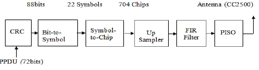
The binary data (72 Bits) packet from the Physical Protocol Data Unit (PPDU) is inserted into the cyclic redundancy check (CRC) block to get 88Bits and then to bit-to-symbol block. Then, every 4 bits are mapped into one data symbol. The symbol-to-chip block performs the Digital Sequence Spread Spectrum (DSSS) with each symbol is mapped into a 32-chip pseudo-random noise (PN) sequence. These codes (DSSS codes) will be treated as pseudo-noise (PN) sequences because resembles random sequences of bits with a flat spectrum. The main advantage of Digital Signal Spread Spectrum communication technique is to prevent “interference” whether it is intentional or unintentional. The signals modulated with these techniques are hard to interfere and cannot be jammed. An intruder with no official access is never allowed to crack them. Hence, these techniques are used for military purposes.
IJSRR, 7(3) July – Sep., 2018 Page 1331
PROPOSED ZIGBEE DIGITAL TRANSMITTER
Figure 2: Proposed ZigBee Digital Transmitter
The binary data from the PPDU (72 Bits) packet is inserted into the cyclic redundancy check (CRC) block to get 88Bits and then to bit-to-symbol block which maps every four bits into one symbol. Then every symbol is mapped into eight bit p-n chip sequence. Afterward every little bit of p-n sequence is up sampled to match nyquist criteria.
The even bits are up sampled by “up sampler-I”, and odd bits are up sampled by “up sampler- Q”.
These up sampled bits area unit suffered separate Fir filters. The output of up sampler-I is suffered filter Fir-I and output of up sampler-Q is suffered filter Fir-Q. These filters area unit nothing however [*fr1] trigonometric function pulse shaping filter’s that reduces is the digital noise. The output of FIR is 10bit block that is then transmitted to “CC2500” module serially by parallel in serial out (PISO) block. “CC2500” module transmits incoming packets to wireless channel.
5. OBJECTIVES AND METHODOLOGY
5.1 Objectives
A ZigBee transmitter is to be designed for PHY and MAC layers for an acknowledgement frame. This design is going to be modeled using Verilog HDL and simulated using Xilinx ISE simulator. The performance of operation of the proposed design should satisfy the theoretical specifications and will be verified with the simulation results and then implemented on Spartan 3E FPGA Board.
1. The objective is to reduce number of slices, Flip Flops and Look Up Tables (LUT’s) compared to the conventional system.
IJSRR, 7(3) July – Sep., 2018 Page 1332
5.2 Methodology
The past many years have witnessed a fast development within the wireless space network. Wireless networking has been centred on high speed and long varies applications. ZigBee may be a customary that defines the set of communication protocols for low data rate short-range wireless networking. This is often the most mo]. tivation of development of Zigbee customary. The quality ZiBee Alliance1. The Zigbee customary has adopted IEEE 802.15.4 Physical Layer (PHY) and Medium Access Control (MAC) protocols3 The PHY layer supports 3 frequency bands: a.868 MHz band with 1 channel, a 915 MHz band with 10 channels and a 2.45 GHz band with 16 channels. The word digital encompasses a special place in society. There are two reasons which causes development of digital solution, first is good digital system design and another is modeling techniques. More additional developments have created and introduced VLSI so as to enhance speed of operation, to scale back size of the design, enhancements in sure thing of the circuit. Digital Zigbee Transmitter contains of Cyclic Redundancy Check Block, Bit-to-symbol block, Symbol-to-chip block, Up-Sampler, FIR Band Pass Filter block and Parallel in Serial out Block. The work here is to indicate however we will style Zigbee transmitter with its specifications by using Verilog with less number of slices and Look up tables (LUTs).
IJSRR, 7(3) July – Sep., 2018 Page 1333
Figure 3. The acknowledgment frame
IJSRR, 7(3) July – Sep., 2018 Page 1334
RESULTS AND DISCUSSION
6.1 Design Utilization Summary of Zigbee Digital Transmitter
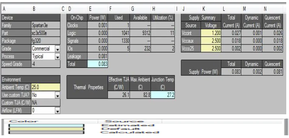
Figure 4: Design Summary
Device utilization is the hardware and logic circuitry required to implement the design.
The Proposed Digital Transmitter Design summary is shown in the figure 3. The Proposed
transmitter has utilized Slices up to 689 out of 4656, Flip Flops about 712 from 9312 and LUTs
about 937 from 9312.
6.2 RTL Schematic of Zigbee Transmitter (Top Module)
Figure 5. RTL Schematic Diagram of Top Module
IJSRR, 7(3) July – Sep., 2018 Page 1335
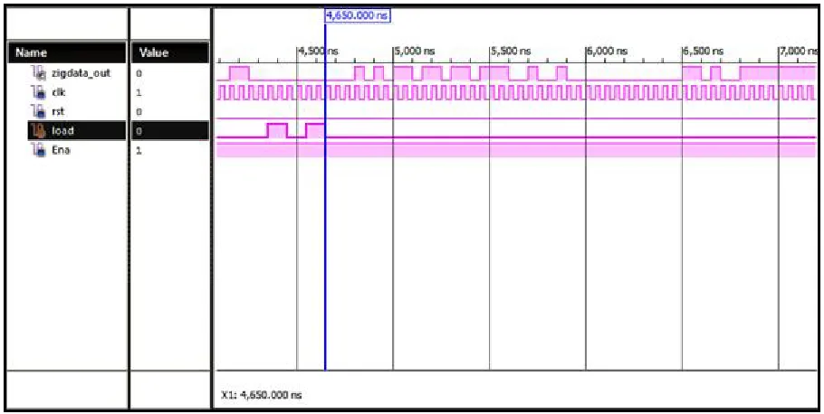
input ports are comprised of Ena, Load and Rst. The output port is Zigdata_out. When clock,Ena
and Load is high and rst is 0 the inputs are applied to get the output.
6.3 RTL Schematic Diagram
Figure 6: RTL Schematic Diagram
T
he digital transmitter is shown in the figure 2. It clearly shows the various modules of
the ZigBee digital transmitter. Starting with MAC and PHY formats for Acknowledgment frame
such as Preamble Sequence, Start of Frame De-limiter
(
SFD), Frame Length (Frame Length),
Frame Control, Frame Check Sequence, CRC block, Bit2Symbol Block, Symbol2Chip Block,
Two Up sampler Blocks one for Odd Samples and another for Even samples Block, Two FIR
blocks, one for Odd bits and second one for even bits and Parallel in Serial Out Block which
produces a stream of bits which are transmitted by a transmitter.
IJSRR, 7(3) July – Sep., 2018 Page 1336 Figure 7: Output Simulation showing First bit delay
Figure 8: Output Simulation showing Last bit delay
IJSRR, 7(3) July – Sep., 2018 Page 1337
6.5 Results Comparison
Table 2. Results Comparison Table
References Slices Flip Flops LUTs Clk Frequency
No % No % No %
4 1630 35 1024 11 2794 30 250KHz & 2MHz
Proposed 689 14 712 7 937 10 20MHz
Table 2 summarizes the implementation specifications obtained for conventional partially
designed ZigBee Digital Transmitter, completely designed ZigBee Digital Transmitter and
Proposed ZigBee Digital Transmitter.
Reference
3.ZigBee with all the modules i.e., CRC, Bit-to-Symbol, Symbol-to-Chip,
OQPSK and Pusle Shaping Modules used Slices up to 1630 out of 4656 , Flip Flops about 1024
from 9312 and LUTs about 2754 from 9312 with clock frequency of 25MHz,
Proposed ZigBee Digital Transmitter was designed completely in all aspects and was
found that the proposed ZigBee Transmitter has utilised Slices up to 689 out of 4656, Flip Flops
about 712 from 9312 and LUTs about 937 from with clock frequency of 20MHz.
Therefore, it is proved that the design area of Proposed ZigBee Transmitter in terms of
Slices, Flip Flops Look Up Tables is less than the conventional ZigBee Transmitter.
Figure 9: Slices Comparison Chart 1630 689 0 200 400 600 800 1000 1200 1400 1600 1800 [4] Proposed N o. of S li ce s
IJSRR, 7(3) July – Sep., 2018 Page 1338
The Column chart for the slices utilized by the conventional system and proposed
system is shown in the Figure: 9. It shows the clear difference between the slices utilized by the
conventional system and the proposed system. According to the above figure the proposed
system has less number of Slices compared to the Conventional system.
Figure10.: Flip Flops Comparison Chart
The Figure 10 shows the Flip Flops utilized by the conventional system and proposed
system. It shows the clear difference between the slices utilized by the conventional system and
the proposed system. According to the above figure the proposed system has less number of Flip
Flops compared to the Conventional system.
1024
712
0 200 400 600 800 1000 1200
[4] Proposed
N
o.
of
F
li
p
F
lop
s
IJSRR, 7(3) July – Sep., 2018 Page 1339 Figure 11: LUTs Comparison Chart
The Figure 11 shows the Look Up Tables (LUTs) utilized by the conventional system i.e.,
[4] and Proposed system. It shows the clear difference between the LUTs utilized by the
conventional system and the proposed system. According to the above figure the proposed
system has less number of LUTs compared to the Conventional system.
6.6 Power Estimation
Figure 12: Power Estimation 2794
937
0 500 1000 1500 2000 2500 3000
[4] Proposed
N
o.
of
L
U
T
s
IJSRR, 7(3) July – Sep., 2018 Page 1340
Power utilised by the Complete ZigBee Digital Transmitter including the board power is
shown in the figure 10. The power was estimated by Xilinx XPower Tool. Light blue color shows
the estimated power, yellow color shows the default power and the grey color gives the actual
calculated power consumed by the ZigBee Digital Transmitter.
6.7 Conclusion:
The Design of Digital Transmitter in 2.4GHz band for ZigBee Applications based on
Verilog is clearly discussed in this research. The CRC behaviour and Bit-to-Symbol, Symbol to
Chip, Up-Sampler, FIR and Parallel in Serial Out blocks have been characterized using Verilog.
It can be concluded that a complete ZigBee Digital Transmitter has been characterized and
synthesized in the initial work. The synthesis is done by using XILINX ISE and targeted for
SPARTAN 3E FPGA. The synthesis results obtained for the proposed method shows reduced
Slices, Flip Flops and LUTs when compared to previous best existing conventional works. Hence
the proposed method proves the more efficient in area. The power
results have been obtained
from Xilinx XPower Tool. In the previous conventional works Power was not calculated so my
work is a novel one.
ACKNOWLEDGEMENT
I would also like to acknowledge the enthusiastic Co-Supervisor Dr. Rajendra Naik,
Professor, Department of ECE, University College of Engineering, Osmania Univeristy for his
valuable guidance and support extended throughout the research. It is his co-operation and
kindness, that I could complete my research paper. My grateful, appreciation for him, for
providing Xilinx lab facility and other facilities during the researcH
REFERENCES
1.
Camilli, A., Cugnasca, C.E. , Saraiva, A.M. , Hira-kawa, A.R. andCorrêa, P.L. Anatomy
ofan application for precision agriculture, Computers and Electronics in Agriculture.
2007; 58: 25-36
IJSRR, 7(3) July – Sep., 2018 Page 1341