LETTER
Effects of a micro pattern on Cu alloy
electrodeposition and its application as an oil
detector
Jae Min Lee
1,2and Jong Soo Ko
1*Abstract
In this study, the effects of open area ratio (OAR) variations by micro-patterns on Cu alloy electrodeposition were analyzed experimentally. To change the OAR of the samples, a strip-type micro-pattern was formed on a substrate through a photolithography process. Moreover, the OAR was controlled by adjusting the distance of the stripe pat-tern to a width of 20 μm. When electrodeposition was applied on a non-patpat-terned substrate with an OAR of 100%, a pillar-type Cu alloy structure was produced. In addition, when the OAR was decreased to 40%, the height of the Cu alloy structures was increased. However, when the OAR was decreased to 20%, no electrodeposited structures were formed. To confirm the industrial effectiveness of the electrodeposited structures on a micro-pattern, the Cu alloy electrodeposited structures were applied to the formation of an oil detector.
© The Author(s) 2016. This article is distributed under the terms of the Creative Commons Attribution 4.0 International License (http://creativecommons.org/licenses/by/4.0/), which permits unrestricted use, distribution, and reproduction in any medium, provided you give appropriate credit to the original author(s) and the source, provide a link to the Creative Commons license, and indicate if changes were made.
Background
Micro- and nanostructured metal substrates are widely used in various industrial fields including surface modi-fication, anti-corrosion, solar cells, and microelectronic interconnection [1–5]. Representative methods for pro-ducing metallic micro-and nanostructured substrates include an electroplating method using a micro- or nano-patterned mold, a dry or wet etching method using an etching barrier, and laser machining [6–8]. However, these methods require considerable time and cost for producing metallic microstructures.
To overcome this problem, an electrodeposition tech-nique without a mold was proposed [9, 10]. Using this electrodeposition method, the time and cost required for the fabrication of metallic microstructures can be sig-nificantly reduced. Moreover, electrodeposition methods allow the formation of various shapes of the metal alloy structure by controlling simple variables such as the stir-ring rate, temperature, and applied current density [11,
12].
Representative materials for producing a metallic microstructure through an electrodeposition technique include Cu, Au, Ni, Ag, and Sn [11–16]. Among them, Cu and Cu alloys are excellent engineering materials, and have significant advantages including a low chemical reactivity, low cost, high electrical conductivity, and good thermal conductivity [12, 17]. Therefore, many research-ers have been studying methods for producing Cu or Cu alloy microstructures through an electrodeposition technique. However, most researches on Cu or Cu alloy microstructure formation have utilized non-patterned substrates.
In this paper, we produced a Cu alloy microstructure on a stripe-type micro-patterned substrate. Moreover, the effects of the open area ratio (OAR) variations from a micro-pattern on the formation and growth of Cu alloy structures was analyzed. Furthermore, to evaluate the effectiveness, our research group applied a Cu alloy elec-trodeposited structure on a micro-pattern for the fabri-cation of an oil detector.
Experimental
The copper electrodeposition solution used was com-posed of 0.6 M CuSO4·5H2O (Dae Jung, Korea) and
1.0 M boric acid (H3BO3, Dischem, USA). To apply the
Open Access
*Correspondence: [email protected]
1 Graduate School of Mechanical Engineering, Pusan National University,
electrodeposition, an electroplating machine (Sung Won Forming, Korea) was used. In addition, a copper plate (Daeguang metal, Korea) with dimensions of 3 × 3 cm was used as an anode. For the fabrication of a cathode, Cr (50 nm) and Cu (500 nm) were deposited sequen-tially on a silicon wafer (Win Win Tech, Korea). The sili-con wafer was then diced to a sample size of 1 × 1 cm. In addition, the solution temperature, stirring rate, and applied current density were maintained at 60 °C, 200 rpm, and 50 mA/cm2, respectively. For the stirring of
the solution, a magnetic stir bar (Cowie technology, UK) with a diameter of 0.8 cm and length of 5.0 cm was used. The morphology of the electrodeposited structure was observed using a scanning electron microscope (SEM) (S-4800, HITACHI, Japan). Furthermore, an energy dis-persive spectroscope (EDS) (7593-H, HORIBA, Japan) was used to analyze the composition of the fabricated samples.
Results and discussion
Results of Cu alloy electrodeposition on non‑patterned substrate
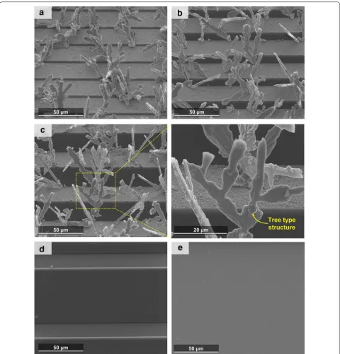
Figure 1 shows the results of Cu alloy electrodeposition on a non-patterned substrate with and without stirring. When stirring was not applied, a dome or polygon-type structure was formed (Fig. 1a). According to previous research, the electrodeposited structures are composed of Cu and Cu2O [18, 19]. Moreover, the EDS
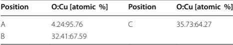
analy-sis results in Table 1 show that the formed dome-type structure consisted mainly of Cu. On the other hand, the polygonal structure mainly consisted of Cu2O.
When electrodeposition was conducted using a CuSO4·5H2O solution, Cu and Cu2O were deposited at
the same time. The electrodeposition mechanism of Cu
and Cu2O can be described through Eq. 1 (reduction of
Cu2+ ions) and Eq. 2 (reduction of Cu+ ions) [11, 19].
Equation 1: Reduction of Cu2+ ions
Equation 2: Reduction of Cu+ ions
As shown in Eqs. 1 and 2, Cu2+ ions in a CuSO 4·5H2O
solution can be precipitated into Cu2O or Cu. Moreover,
the deposited Cu2O can be reduced to Cu metal through
Eq. 2a. However, when Cu2O structures grow larger
before a reduction, a larger Cu2O structure has difficulty
converting into Cu metal [18]. Because the resistance of the Cu2O is higher than that of Cu, a charge is difficult to
transfer to large Cu2O structures. On the other hand, a
small Cu2O structure is easily converted into Cu through
Eq. 2a. Therefore, when electrodeposition is applied using a CuSO4·5H2O solution, a Cu and Cu2O structures
are formed separately.
Figure 1b shows the shape of the electrodeposited structure formed when the solution was stirred at
(1a)
Cu2++ H2O +2e−→ Cu2O + 2H+
(1b) Cu2+
+ e−
→ Cu+
(2a) Cu2O + 2H++ 2e−→ Cu + 2H2O
(2b)
Cu+
+ e−
→ Cu
Fig. 1 SEM image of the substrates electrodeposited with Cu alloy a without and b with stirring (200 rpm)
Table 1 O-Cu composition ratio at each position shown in Fig. 1
Position O:Cu [atomic %] Position O:Cu [atomic %]
200 rpm during the electrodeposition. When the solution was stirred, a pillar-type electrodeposited structure was generated. The promotion of Cu2O deposition through
stirring is regarded as the reason for the pillar structure formation.
Because the equilibrium electrode potential of Cu2O
(0.347 V) versus a standard hydrogen electrode is higher than that of Cu (0.297 V), Cu2+ ions in an
electrodepo-sition solution are usually precipitated into Cu2O rather
than Cu [19]. However, when the diffusion rate of Cu2+
ions is lower than the charge supply rate, the deposited Cu2O is actively converted into Cu through Eq. 2 instead
of insufficient Cu2+ ions. Under this condition, the
depo-sition of the Cu2O is controlled through the diffusion of
the Cu2+ ions. Moreover, Cu
2O deposition is
concen-trated at the top of the electrodeposited structure with a short diffusion distance.
Therefore, when Cu2O deposition is controlled by the
diffusion of the Cu2+ ions, Cu
2O deposition promotes a
vertically oriented growth of the electrodeposited struc-tures. On the other hand, the reduction of the Cu2O is
not affected by the diffusion of the Cu2+ ions. Cu
pre-cipitation through a reduction in Cu2O can be achieved
throughout the entire area of the Cu2O structure.
There-fore, a reduction in Cu2O promotes isotropic growth of
the electrodeposited structures.
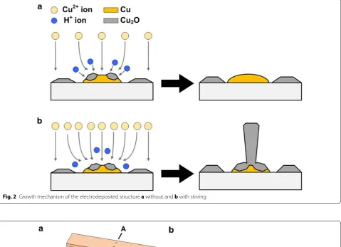
As shown in Fig. 2a, when the solution is not stirred, the deposited Cu2O is actively reduced to Cu.
Moreo-ver, under this electrodeposition condition, through the isotropic growth of the electrodeposited structures originating from the reduction in Cu2O, a dome-type
electrodeposited structure is formed. However, when the solution is stirred during the electrodeposition, the diffusion rate of the Cu2+ ions is increased. This
results in a suppression of the Cu2O reduction.
There-fore, a pillar-type electrodeposited structure achieved through a vertically oriented growth can be formed when the solution is stirred (Fig. 2b). This growth mechanism is proven based on the EDS analysis results, which indicate that the surface of the pillar is composed of Cu2O (Table 1). However, as mentioned,
the dome type structures are main composed of Cu metal.
Results of Cu alloy electrodeposition on micro‑patterned substrate
To analyze the effects of the OAR variations, a stripe-type micro-pattern was formed using a photolithography process. OAR is the ratio of the electrodeposited area to the total top surface area of the sample, which is defined in Eq. 3.
(3)
Open area ratio = W
W + D × 100%
Figure 3 shows the shape of the micro-patterned sam-ples. Five different samples with an OAR of 100, 80, 60, 40, and 20%, respectively, were produced. To adjust the OAR, the distance of the stripe pattern (D) was fixed to 20 μm, and the width of the patterns was controlled. Table 2 shows the detailed design dimensions of the fab-ricated samples. The OAR of the non-patterned substrate was 100%.
Figures 1b and 4 show the shape of the Cu alloy elec-trodeposited structure as a function of the OAR. To avoid any influence from the thickness of the electrodeposited layer, the applied current density of the electrodepos-ited area was fixed to 50 mA/cm2. Therefore, the applied
current was varied as a function of the OAR (Table 2). Moreover, the electrodeposition time, stirring rate, and temperature of the solution were maintained at 4 min, 200 rpm, and 60 °C, respectively. When the OAR of the samples was decreased from 100 to 40%, the height of the electrodeposited structures tended to increase. In addition, when the electrodeposition was applied on the stipe-type micro-patterned substrate, the development of the electrodeposited structure was concentrated at the edge of the micro-patterns.
As shown in Table 2, when the applied current density is fixed, the applied current is proportional to the OAR. Therefore, the charge supply rate is decreased with a decrease in the OAR. As mentioned, the decrease in the charge supply rate leads to the suppression of the Cu2O
reduction. This resulted in the promotion of a vertically oriented growth of the Cu alloy electrodeposited struc-ture. Moreover, when the micro-pattern was formed, the deposition of the Cu2+ ions located outside the
pat-tern (marked as *, in the hatched area in Fig. 5a) was concentrated at the side edge of the patterns. Therefore, when the OAR was decreased to 40%, the height of the structures was increased and the formation of the elec-trodeposited structures was concentrated at the edge of the micro-patterns.
In addition to the variations in size, when the OAR was decreased to 40%, tree-type electrodeposited struc-tures were actively formed (Fig. 4c). This phenomenon is thought to have originated from the growth rate increase of the electrodeposited structure. Figure 5 shows the for-mation mechanism of the tree-type structures. When the height of the electrodeposited structures was increased, the deposition of the Cu2+ ions was concentrated at the
top-edge of the structure with a short diffusion distance (indicated by the red circle in Fig. 5b). This phenome-non can trigger the formation of new branch structures. The repetitive formation of branches produces the tree-shaped Cu alloy micro-structure (Fig. 5c).
have originated from the applied decrease in poten-tial. Because the applied potential is proportional to the applied current, the applied potential is decreased with a decrease in the OAR (Table 2). For a reduction of the Cu2+ ions, a negative potential below the
reduc-tion potential needs to be applied. When the OAR is decreased to 20% (i.e., the applied current is 10 mA), an
Fig. 2 Growth mechanism of the electrodeposited structure a without and b with stirring
Fig. 3 Shape of the stripe-type micro pattern. a Perspective view, b cross-sectional view along to A–A
Table 2 Design and electrodeposition conditions of the samples as a function of the OAR
Open area ratio (%) 100 80 60 40 20
insufficient potential is applied to the sample for Cu or Cu2O deposition. Figure 4e proves this phenomenon.
Figure 4e shows the electrodeposition results of the non-patterned substrate when the applied current is 10 mA. In this case, no electrodeposited structure was formed.
Application as an oil detector
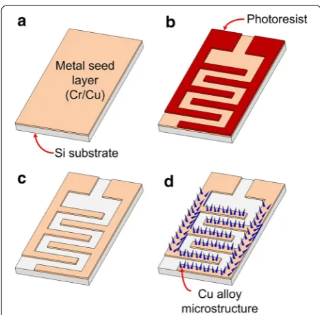
To confirm the industrial effectiveness of a Cu alloy structure on a micro-patterned substrate, the Cu alloy structures on the pattern were applied to an oil detector formation. Figure 6 illustrates the fabrication process of
this oil detector. First, Cr (20 nm) and Cu (500 nm) were sequentially deposited on the silicon substrate (Fig. 6a). Second, PR patterns composed of two stripes were formed (Fig. 6b). Next, metal wet etching and PR removal were sequentially applied (Fig. 6c). Finally, Cu alloy elec-trodeposition and a plasma-polymerized fluorocarbon (PPFC) coating process were applied (Fig. 6d). Figure 7
shows a camera image of the fabricated oil detector and an SEM image of the Cu alloy structure on the stripe-type metal patterns.
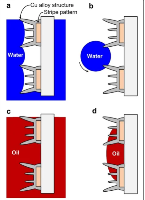
The fabricated oil detector consisted of two stripe-type metal patterns with Cu alloy electrodeposited structures. In addition, the patterns with Cu alloy structures were not electrically connected. Therefore, the stripe patterns created a capacitance. In addition, the stripe patterns with PPFC-coated Cu alloy structures showed super-hydrophobic and oleophilic properties (Fig. 8a and b). Therefore, when the stripe patterns with Cu alloy struc-tures were inserted into water, the water did not pen-etrate the space between the two stripe patterns owing to their hydrophobicity [20] (Fig. 9a). Moreover, when pat-terns with Cu alloy structures were pulled out from the
Fig. 5 Formation mechanism of the tree-type electrodeposited structures. a The early electrodeposition stage, b electrodeposition after the forma-tion of the pillar structures, c the formation of the branch structures
Fig. 6 Fabrication process of the oil detector. a Metal seed layer deposition, b photolithography, c metal wet etching and PR removal,
wafer, the residual wafer droplets were easily removed from the surface (Fig. 9b).
On the other hand, when the oil detector was inserted into oil, the oil was easily diffused into the space between the two stripe patterns (Fig. 9c). Furthermore, when the detector was pulled out, residual oil remained in the space between the stripe patterns (Fig. 9d), which resulted in a variation of the detector’s capacitance. Owing to this phenomenon, Cu-alloy electrodeposited stipe patterns can be used as an oil detector.
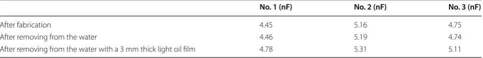
We fabricated three different oil detectors with dimen-sions of 1.5 × 2.3 cm2. As mentioned before, the oil
detector formed has two metal stripe patterns. The dis-tance and width of the strip patterns were designed to be 50 and 400 μm, respectively. When the oil detector was inserted into water at a 10 cm depth, and then removed from the water, the capacitance of the detector was not varied. However, when the oil detector was inserted into water with a 3 mm thick light oil film, the capacitance of the oil detector was varied even after the detector was removed from the wafer with oil film. Table 3 shows the measurement results for a variation in capacitance. The measurement results prove that a Cu alloy structure on a micro-pattern can be applied as an oil detector.
Conclusion
In this paper, the effects of the OAR variations using micro patterns on Cu alloy electrodeposition were ana-lyzed. To discover the influence of the OAR variation, a
Fig. 7 Fabricated oil detector, a camera image of the detector, b SEM image of the Cu-alloy electrodeposited stripe pattern of the detector
Fig. 8 Contact angle measurement results for a water and b light oil droplets
stripe-shaped micro-pattern was formed through the lithography process. By adjusting the distance of the stripe patterns with a width of 20 μm, samples with an OAR of 100, 80, 60, 40, and 20% were produced. The applied current density of the electrodeposited sample was fixed to 50 mA/cm2. Under this condition, when
the OAR was decreased from 100 to 40%, the height of the electrodeposited structures showed a tendency to increase. On the other hand, no electrodeposited struc-ture was formed when the OAR was 20%. To confirm the industrial effectiveness of a Cu alloy electrodeposited structure on a micro-pattern, Cu alloy structures on a stripe-type micro-pattern were applied to the fabrication of an oil detector. The fabricated oil detector is able to detect an oil film of 3 mm in thickness by measuring the variations in capacitance.
Authors’ contributions
JML participated in design, fabrication, and test the device and drafted the manuscript. JSK conceived of the study, reviewed all test methods and results, and finalized the drafted manuscript. Both authors read and approved the final manuscript.
Author details
1 Graduate School of Mechanical Engineering, Pusan National University,
Busandaehak-ro 63 beon-gil, Geumjeong-gu, Busan 48075, South Korea.
2 Research & Development Team 1, Hanwha Corporation Gumi Plant, 264-36
Sanho-daero, Gumi, Gyeongsangbuk-do, South Korea.
Acknowledgements
This work was supported by a 2 year Research Grant of Pusan National University.
Competing interests
The authors declare that they have no competing interests.
Received: 5 October 2016 Accepted: 17 October 2016
References
1. Han JT, Jang Y, Lee DY, Park JH, Song SH, Ban DY, Cho K (2005) Fabrication of a bionic superhydrophobic metal surface by sulfur-induced morpho-logical development. J Mater Chem 15:3089–3092
2. Zhang W, Yu Z, Chen Z, Li M (2012) Preparation of super-hydrophobic Cu/ Ni coating with micro-nano hierarchical structure. Mater Lett 67:327–330 3. Liu T, Yin Y, Chen S, Chang X, Cheng S (2007) Super-hydrophobic surfaces
improve corrosion resistance of copper in seawater. Electrochim Acta 52:3709–3713
4. Jeong S, Garnett EC, Wang S, Yu Z, Fan S, Brongersma ML, Cui Y (2012) Hybrid silicon nanocone–polymer solar cells. Nano Lett 12:2971–2976 5. Zhou Y, Sreekala S, Ajayan PM, Nayak SK (2008) Resistance of copper
nanowires and comparison with carbon nanotube bundles for intercon-nect applications using first principles calculations. J Phys Condens Matter 20:095209
6. Lee JM, Lee SM, Jung PG, Ko JS (2011) Superhydrophobic nickel micro-mesh with microfences. J Micromech Microeng 21:105003
7. Dubey AK, Yadava V (2008) Laser beam machining—a review. Int J Mach Tools Manuf 48:609–628
8. Hsu JH, Lai HW, Lin HN, Chuang CC, Huang JH (2003) Fabrication of nickel oxide nanostructures by atomic force microscope nano-oxidation and wet etching. J Vac Sci Technol B 21:2599–2601
9. Lee JM, Bae KM, Jung KK, Jeong JH, Ko JS (2014) Creation of micro-structured surfaces using Cu–Ni composite electrodeposition and their application to superhydrophobic surfaces. Appl Surf Sci 289:14–20 10. Qiu R, Zhang XL, Qiao R, Li Y, Kim YI, Kang YS (2007) CuNi dendritic
mate-rial: synthesis, mechanism discussion, and application as glucose sensor. Chem Mater 19:4174–4180
11. Lee JM, Jung KK, Ko JS (2016) Growth mechanism and application of nanostructures fabricated by a copper sulfate solution containing boric acid. J Electrochem Soc 163:D407–D413
12. Deng Y, Ling H, Feng X, Hang T, Li M (2015) Electrodeposition and charac-terization of copper nanocone structures. CrystEngComm 17:868–876 13. Lee JM, Jung KK, Lee SH, Ko JS (2016) One-step fabrication of nickel
nano-cones by electrodeposition using CaCl 2· 2H 2 O as capping reagent. Appl Surf Sci 369:163–169
14. Gu C, Zhang TY (2008) Electrochemical synthesis of silver polyhe-drons and dendritic films with superhydrophobic surfaces. Langmuir 24:12010–12016
15. Shao W, Zangari G (2009) Dendritic growth and morphology selection in copper electrodeposition from acidic sulfate solutions containing chlorides. J Phys Chem C 113:10097–10102
16. Hu S, Huang W, Li Z (2010) Facile fabrication of 3D dendritic gold nano-structures with an AuSn alloy by square wave potential pulse. Mater Lett 64:1257–1260
17. Wang P, Zhang D, Qiu R (2011) Extreme wettability due to dendritic cop-per nanostructure via electrodeposition. Appl Surf Sci 257:8438–8442 18. Lu Y, Ren Z, Yuan H, Wang Z, Yu B, Chen J (2015) Atmospheric-pressure
microplasma as anode for rapid and simple electrochemical deposition of copper and cuprous oxide nanostructures. RSC Adv 5:62619–62623 19. Ng SY, Ngan AHW (2015) Additive free co-deposition of
nanocrystal-line copper/cuprous oxide by electrodeposition. J Electrochem Soc 162:D124–D128
20. Lee SM, Oh DJ, Jung ID, Bae KM, Jung PG, Chung KH, Ko JS (2009) Fabrica-tion of nickel micromesh sheets and evaluaFabrica-tion of their water-repellent and water-proof abilities. Int J Precis Eng Manuf 10:161–166
Table 3 Capacitance measurement results of the fabricated oil detector
No. 1 (nF) No. 2 (nF) No. 3 (nF)
After fabrication 4.45 5.16 4.75
After removing from the water 4.46 5.19 4.74