Johan Schoeman and Monuko du Plessis
Carl and Emily Fuchs Institute for Microelectronics, Dept. of Electrical, Electronic and Computer Engineering, University of Pretoria, Pretoria, South Africa
Correspondence:Johan Schoeman ([email protected])
Received: 30 March 2019 – Revised: 18 July 2019 – Accepted: 29 August 2019 – Published: 9 October 2019
Abstract. Advances in micromachining have led to the development of microelectromechanical systems (MEMS) devices with suspended structures used in a variety of sensors. Of note for this work are sensor types where two elements exist on the suspended membrane, including examples like air flow and differential pressure detectors, gas detection, and differential scanning calorimetry sensors. Intuitively one would argue that some thermal loss exists between the two elements. However, surprisingly little is documented about this electrother-mal interaction. The work presented here addresses this shortcoming by defining a new parameter set, a matrix of thermal coupling coefficients. They are used within our novel two-port electrothermal model based on the heat flow equation adapted as a linear system of equations. However, the model is only effective with knowledge of these coefficients. We introduce an approach to extract the coefficients using finite-element method (FEM)-based multiphysics simulation tools and revisit and extend our previous method of non-ideal power coupling, this time to extract the coefficient matrix from measured data. Both specialist simulation tools and device manufacturing are very expensive. However, they are the only choices in the absence of an analytic model. A major contribution of this work is the derivation of a model to predict the coefficients by analytic means from the device dimensions and material properties. The research contribution and paper culminate in a comparison of analytic, simulated, and experimentally extracted values of two different devices to verify and demonstrate the effectiveness of the proposed models. The values compare well and show that the best results achieved are approximately 90 % and 70 % thermal linkage respectively for vacuum and atmospheric pressure conditions.
1 Introduction
Electrothermal circuits (ETC) are circuits where the elec-trothermal interaction between components and the substrate is considered. Their analysis has been present in the lit-erature since the early sixties (Matzen et al., 1964; Gray and Hamilton, 1971), but researchers have pursued it with less vigour than the purely electrical counterparts. This is mostly because of the large power consumption constraint associated with their operation (Louw et al., 1977). It was the commercialisation of MEMS manufacturing technolo-gies that gave rise to a vast range of applications for ETC, notably because of the advances in micromachining. This led to high-yield, low-cost manufacturing and massive im-provements in electrothermal performance. These applica-tions have penetrated the industrial, military, and consumer
markets, showing their diversity and the extensive market-ing opportunities they present. Examples include the likes of on-chip sensors for diagnostics (Sisto et al., 2010; Zhang et al., 2009), chemical detection (Corsi et al., 2012; Barritault et al., 2013), thermal conductivity sensors (heat flow sensors and micro-hotplates) (Senesac et al., 2009; Arndt, 2002; Elmi et al., 2008), air flow sensors (Baltes et al., 1998; Johnson and Higashi, 1987; Simon et al., 2001), and thermal imag-ing microbolometers (Akula et al., 2011; Dulski et al., 2013; Castaldo et al., 1996; Liddiard, 2013).
worth mentioning. First, joining a narrow and wide region results in an additional radial thermal conduction compo-nent. The restriction resistance model proposed is very ef-fective and accounts for the additional component under vac-uum conditions (Topaloglu et al., 2010). Second, an elliptical model better accounts for the radial temperature distribution on a suspended membrane in atmospheric pressure condi-tions (Schoeman and du Plessis, 2016). Both methods im-prove conventional models by up to 40 %.
Despite the continued active contributions in the mod-elling of traditional microbolometers, the detailed modmod-elling of more generic dual-element devices, especially the interac-tion between these elements labelled as C in Fig. 1a, is lack-ing. This is surprising considering that these devices have existed for many years (Arndt, 2002; Yoon and Wise, 1994; Klaassen et al., 1995; Baltes et al., 1998). The approach in analytic electrothermal modelling of the detailed thermal in-teraction between the two devices or elements is never very rigorous and the interactions of the suspended elements with one another are mostly unclear. Authors typically assume perfect thermal linkage without mentioning the possibility of imperfect linkage. Furthermore, the electrical feedback net-work will often compensate for the imperfection. One tech-nique offers an analytic solution to the temperature distribu-tion of a thin-film resistor sensor pasted onto a large mass. However, the solutions are complex and time-consuming to solve. The author concludes that the model is useful for cre-ating CAD tools (von Arx et al., 2000). This limits the prac-ticality of the solutions.
It is interesting to note that the absence of an accurate an-alytical model for the electrothermal interaction can likely be attributed to the strength of the FEM simulation method-ologies. However, these tools are very expensive and mostly used to simulate device-level behaviour, although some tools allow the capability of extracting the device model to a circuit-level model that can be used in SPICE-based simula-tion, but at an additional cost. As such, simpler SPICE mod-els have been developed to couple the electrothermal param-eters to electrical ones used in readout circuits for infrared microemitters and microbolometers (Kiran and Karunasiri, 1999; Nazdrowicz et al., 2015; Kim and Ko, 2015). How-ever, we should highlight that the lack of an existing model hampers (i) the understanding and design of optimal ther-mal coupling devices and (ii) the design of effective readout circuits for ETC while accounting for thermal losses. This leaves a research gap that this paper will address. In Sect. 2 of this work we present a novel method to transform com-plex suspended device structures with two resistive elements into electrothermal equivalent microbeams that can be used to determine a matrix of thermal coupling coefficients. This is derived for both vacuum and atmospheric pressure con-ditions. We also propose that a multidimensional heat flow problem can be simplified and described using this set of co-efficients within a linear system of equations modelling an equivalent electrothermal two-port system. Section 3
intro-duces a new simulation methodology to extract the matrix of coefficients. We also extend our experimental method intro-duced previously (Schoeman and du Plessis, 2012) for Ti1 at atmospheric pressure to account for the complete set of parameters required by the latest two-port model. In Sect. 4 we present and compare analytic, simulated, and experimen-tal results for two different devices at two different pressure levels. Finally, we present some conclusions based on the re-sults.
2 Theory and modelling of dual-element suspended plate structures
2.1 Operating principles of suspended devices
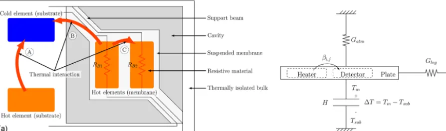
The device structure is similar to conventional microbolome-ters that are created by stacking multiple layers and remov-ing a sacrificial layer by wet etchremov-ing. The structure can be divided into two regions, (i) a membrane that is suspended over a cavity after etching and (ii) support beams to hold the membrane in position. This is illustrated in Fig. 1a. The sus-pended device has a thermal capacity that stores absorbed en-ergy over time and acts as a heat reservoir. It can be heated by applying electrical power to a resistive material deposited on top of the suspended membrane. However, the resulting tem-perature gradient between the membrane and substrate will cause heat to flow from the warmer membrane to the cooler substrate through the support beams and the gas filling the cavity underneath the membrane. These thermal conductive components are referred to as the beam thermal conduction and the gaseous thermal conduction respectively. These in-teractions between the various components are illustrated in Fig. 1b and, with the exception of the thermal linkage com-ponents, are described by a heat flow model for conventional microbolometers blind to IR radiation stated mathematically as (Shie et al., 1996; Galeazzi and McCammon, 2003)
HdTm
dt +|Gatm(Tm−Ta)+{zGleg(Tm−Tsub})
Geff1T
=P , (1)
Figure 1.The operating principles and the thermal model for a generic dual-resistive element device.(a)The device topology highlighting the required components of the device structure and the thermal linkage that exists between the resistive elements.(b)An equivalent heat flow diagram for a generic two-element device. The elements are labelled as the heater and detector, although each element can serve as both.
Geff consists of two components (Eriksson et al., 1997), one of which is a thermal conductance component attributed to heat loss between the suspended membrane and the sub-strate via the support beams referred to as the beam thermal conductance,Gleg. This is the dominant heat loss mechanism under vacuum conditions and is given by (Topaloglu et al., 2010; Niklaus et al., 2007)
Gleg=N
n
X
i=1 kb,i
WB,idth,i
LB,i
, (2)
with i an index to a specific layer, N the number of sup-port beams (typically two or four),kb the effective thermal conductivity of the beam measured in W m−1K−1,W
B the width of the beam measured in metres,dth the thickness of the beam measured in metres, andLBthe length of the beam measured in metres. Accounting for the radial thermal con-ductive component can significantly improve the estimation of the thermal conductivity. The transformed thermal con-ductivity is given by (Topaloglu et al., 2007)
kb0=
π kbLM
π LM+2WMln
π WM 2WB
=
kb
1+2WM
π LMln
π WM 2WB
, (3)
whereLM andWM are the membrane length and width re-spectively.
The second component contributing to Geff is the atmo-spheric or gaseous thermal conductance, Gatm. This is the dominant heat loss mechanism at atmospheric pressure and is given as (Niklaus et al., 2007)
Gatm=kairAeff/dλ, (4)
whereAeff=LM×WM is the area of the membrane in me-tres squared used in conventional methods, kair is the ther-mal conductivity of air at room temperature and pressure
(0.00284 W m−1K−1), anddλis the cavity depth measured
in metres.
Up to this stage, we have only considered the modelling of a conventional microbolometer device. This is a device with two terminals and a single port where power can be ap-plied. Therefore, thermal linkage does not exist. It would be natural to wonder what the impact on the heat flow equation would be when we introduce a second (or multiple) resistive element(s) to the suspended device. This would allow for an additional port to the device through which we can control the plate temperature. The steady-state equivalent of Eq. (1) can be changed to allow for the perspective from thekth in-put as
Gatm+Gleg Tm,k−Tsub
| {z }
Geff1T
=Pk, (5)
wherePk is the biasing electrical power of thekth detector element in Watt andTm,kis the average temperature increase
of the membrane in Kelvin resulting from the applied power componentPk. Furthermore, we should be able to observe
a portion of the power applied to one port on every other port of the device, since the resistive elements all share the same thermal reservoir. This suggests that the elements are thermally linked to each other, and we introduce a parame-ter,βi,j, to describe this thermal linkage. Since each resistive
element will contribute towards a portion of the total change in the average membrane temperature, we propose to model the effective or total thermal increase as a system of linear equations, best described in vector form as
Geff·1T =β·P, (6)
thermal coupling coefficients that exist between the various resistive elements. Here it is assumed thatGeffis a constant scalar value for the developed structure which holds true for symmetric designs.
Therefore, the heat balance equation for a dual-element device in the steady state can be given by
Geff· 1T1 1T2 =
β1,1 β1,2 β2,1 β2,2 · P1 P2 , (7)
from which we can easily solve the respective individual ele-ment average temperature increases ifβis known. The latter is relatively simple to determine from simulation and experi-mentally, as shown in Sect. 3. However, the analytic approach proves more challenging, as elaborated on next.
2.2 An analytic solution for the thermal coupling coefficients
Researchers have published comprehensive techniques for modelling the electrothermal behaviour of device structures with various degrees of similarity to our own. Examples in-clude temperature profiling by solving the general heat flow partial differential equation (PDE) first developed and solved by Fourier, reducing dimensionality for specific applications by transformation, applying lumped thermal element analy-sis, and considering thermal coupling in the context of See-back and Peltier effects. As expected, the intent is often to find one or more mechanical properties. We use similar meth-ods that culminate in a robust approximate model to describe the electrothermal effect. The novel model consists of three parts: (i) finding the thermal coupling coefficients for two points on a microbeam, (ii) transforming between the mi-crobeam and a more complex structure, and (iii) increasing the number of points by averaging over the entire resistive length. Each part is elaborated on next in a separate subsec-tion.
2.2.1 Determine the coupling coefficient between two points on a microbeam
A number of examples exist where the steady-state heat transfer, well known to be governed by a second-order PDE, is solved analytically to find the temperature profile of a microbeam, cantilever, or similar rectangular MEMS type structures, which is then in turn further developed to solve some mechanical property, be it displacement, de-flection, dampening, stresses, or elasticity (Chow and Lai, 2009; Kokkas, 1974; Huang and Lee, 1999; Yan et al., 2004; Mankame and Ananthasuresh, 2001). We use a similar ap-proach to derive an expression for the newly proposed ther-mal coupling coefficients.
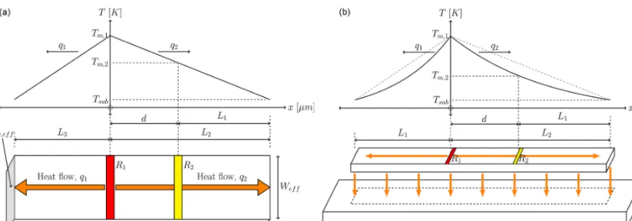
First, consider a microbeam with two resistive components as illustrated in Fig. 2a.R1 is heated to a specific tempera-tureTm,1that results in two heat flow vectors. One of these,
q2, flows throughR2that experiences an increase in tempera-ture in response. We know that under vacuum conditions the simplest form of a second-order linear homogeneous differ-ential equation describes heat diffusion, given by ∂2T
∂x2 =0. The differential equation is solved by double integration and a particular solution is found from the general solution. The former is given by
T(x)=Tm,1− T
m,1−Tsub L2
x. (8)
We define a new parameter, the thermal coupling coeffi-cientβ2,1, as a ratio of temperature differences. Substitution of the parameters in Fig. 2a into Eq. (8) yields
β2,1= 1T2 1T1
=Tm,2−Tsub
Tm,1−Tsub
= L1
d+L1
. (9)
The problem is more complex when the device operates at atmospheric pressure since an additional gaseous thermal conduction component exists. This is illustrated in Fig. 2b. The best approach to derive a solution is to model the prob-lem as a distributed thermal resistance network withrs and
gairthe unit components for the solid thermal resistance and the gaseous thermal conduction respectively. The tempera-ture distribution is found by solving the standard form of a second-order linear homogeneous differential equation if the system is in steady state. This is given by
d2T(x)
dx2 −K·T(x)=0, (10) withK=rsgair. The roots of the quadratic equation may be solved and, after defining boundary conditions, the particular solution can be shown to be given by
T(x)= Tm,1−Tsub
e−
√
K·x. (11)
It is insightful to consider the parameterLch, the charac-teristic thermal length governing the exponential decay ob-served for the temperature over distance, given by
Lch= 1 √
K
=√ 1
rsgair = s dλ kair X i
kb,idth,i (12)
for a multilayered device structure and approximately 10 µm for our devices. The thermal coupling coefficient fol-lows from the definition earlier in Eq. (9) and is given by
β2,1= T(L1) T(L2)
=e−
√
Figure 2.A microbeam with two resistive strips and the relevant dimensions, along with the expected temperature profiles over the length of the bar.(a)The temperature profile through a microbeam when heat flow occurs only through the microbeam is typical under vacuum conditions.(b)The temperature profile through a microbeam when heat flow occurs through both the solid components of the microbeam, as well as the medium (either a gas or a fluid) between the microbeam and a heat sink.
It should be clear that the coupling coefficient depends on the ratio of the separation distance between the resistive el-ements and the characteristic length of the microbeam in an exponential manner. The thermal coupling can be maximised by reducing the separation distance of the resistive elements in a design.
2.2.2 Transform between microbeams and suspended plate structures
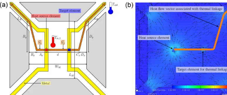
It is also desirable to calculate thermal linkage for more com-plex device geometries. This should be possible if the more complex geometry can be transformed into a simpler mi-crobeam and the thermal coupling coefficients of the previ-ous section is applied. In general, transformations between device geometries are not new and examples include multi-dimensional structure transformation into cylindrical coordi-nates (Khan and Falconi, 2013; Sberveglieri and Hellmich, 1997; Simon et al., 2001). Our approach is quite different and is based on an equivalent heat flow vector analysis.
We propose that the equivalent heat flow of interest from a specific heat source point through a specific target element will occur only along a single vector as illustrated in Fig. 3b. This should be intuitive, but can also be observed from the supporting FEM simulation result of Fig. 3b. The simulation result also shows an infinite amount of additional heat flow vectors, but recall that the desired solution is the single vector flowing through the target element. Therefore, we only need to consider the vectorV2.
Closer inspection reveals that V2 extends from the heat source towards the closest point on the second resistive el-ement where thermal linkage occurs, after which the vector extends by some fraction Cmpast R2. It changes direction towards the connection between the support beam and the
membrane and finally extends along the support beam to-wards the substrate.V2is stated mathematically as
V2=d+C+D+LB (14)
and the distance between the heat source point and the sub-strate is calculated by
kV2k =d+
Cx, Cy+
Dx, Dy +
LB,x, LB,y =d+Cm
W M
2 −
d
2
+
s
(1−Cm)
W M 2 −
d
2 2
+ L
M 2
2 +LB
=L2, (15)
whereCmis a proportionality constant (a typical value is 0.5)
that describes the depth of penetration ofCin thexdirection beforeV2changes direction,WMis the width of the mem-brane,LB is the length of the support beam, and d is the separation distance between the source and target points. It should become immediately clear after inspection of Eq. (15) that this vector is in the formL2=d+L1. This can be used to relate a suspended plate structure, like a microbolometer, to the microbeam of the previous section and allows for the calculation ofL1, a microbeam parameter, as a function of the plate dimensions.
Figure 3.A graphical illustration of the heat flow vector of interest that results in thermal linkage for a dual-element suspended plate with four support beams. A simulation model with a simplified elemental heat source supports the proposal. (a)A structural overview of the device with the relevant dimensions indicated. The proposed vectors are indicated by the orange arrows, while a single heat source element is indicated as a red square and the target element on the opposing resistor is indicated by a blue square.(b)A simulation result showing the heat flow vectors from a single source element as well as the proposed heat flow vector (indicated by the orange arrow) resulting in the thermal linkage between the heat source and target.
is the same as that of the equivalent microbeam. This occurs if the microbeam has an effective width given by
Weff=
WM(1x1+1x2) 1x1+1x2
WM
WB
, (16)
where1x1=LM2−d+d=LM2+d and1x2=LB.
2.2.3 Determine an average coupling coefficient over the entire resistor length
The model components developed thus far for thermal link-age between two single points are not very useful until the concepts are extended to apply to heaters and detectors with more practical lengths. As such, we introduce the notion of dividing the heater and detector elements into unique regions and applying an averaging mechanism. To classify a region as unique, we identify the parts of the heater that have a con-stant separation distance to the detector. Every such length with a unique separation distance would make up a unique region. A number of ksuch regions can exist for a device, but the thermal linkage is optimised by reducing the number of regions, withk=1 being optimal. We illustrate the con-cept of regions in Fig. 4 and show examples in Sect. 2.3. We can use the entire length of a region as part of the weighting coefficient,lreg,i/LR1.
Furthermore, a length of the heater element might be as-sociated with more than one region. This increases compu-tational complexity, but when considering Eqs. (9) and (13) we realise that the increase in separation distance dramati-cally reduces the thermal linkage. We can simplify the prob-lem and find an approximate solution by only considering the
region with the smallest separation distance for any length of the heater. Therefore, a region only needs to be coupled to its closest neighbouring region on the alternate resistor, with the remaining regions considered insignificant. These considera-tions result in an averaging algorithm given by
β2,1≈
k
X
i=1 lreg,i
LR1
β2,1 di,jn
, (17)
withjnbeing the single nearest neighbour only of the par-ticularith region. This results in a computational reduction, often to the extent that the thermal coupling can be computed quickly by hand without the need for simulation. An example is provided at the end of the next section.
2.3 Device designs
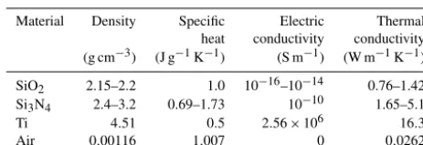
The material properties of the materials used to construct the suspended devices play a significant role in the device per-formance parameters. Notably, the thermal conductivity,ki,
of the materials used to construct the support beams plays a role in the thermal conductance,Gleg, especially that of sil-icon nitride in typical suspended plate designs. The various material densities,ρi, and specific heat,ci, play a major role
in the thermal time response,τ, and the thermal capacity,H, of the devices. The relevant properties are summarised in Ta-ble 1.
sions.
Device WB LB Ni WM LM WR LR (µm) (µm) (µm) (µm) (µm) (µm) (µm) Ti1 15 75 2 63 50 3 490 Ti2 8.5 4 4 50 53 3 210
and (iii) the length of the coupling region between the resis-tive elements,di,j. The length and the width of the second
Ti thin-film resistor are not indicated, but they are defined in the same way as for the first resistor. A summary of the device designs and their dimensions and surface characteris-tics are provided in Table 2, while the linkage parameters are compared in Table 3.
A device (Ti1) optimised for a very high thermal coupling coefficient is illustrated in Fig. 4a. The device features two Ti thin-film resistors with a separation distance dA=3 µm over the entire length of the resistorsLR,1=LA=460 µm. A second device, Ti2, offers a high thermal coupling co-efficient and is illustrated in Fig. 4b with the device di-mensions specified in Table 2. The device has a resistance length LR,1=210 µm and is divided into three unique re-gions (A, B, and C) with region lengthsLA=155,LB=38, andLC=8.5 µm and separation distancesdA=3, dB=9, anddC=15 µm.
3 Methodology
3.1 Approach followed in the simulation study
Multiphysics simulation platforms are highly effective in simulating 3-D device structures. We opted to use Coven-torware, an industry leading multiphysics MEMS simulator, for the study. The standard material properties database of the simulation software is used and the values correspond closely to those in Table 1. A thermomechanical solver is se-lected to simulate thermoelectric physics in the steady state by applying an electrical potential to the gold contacts of the device as a boundary condition and then to investigate the re-sulting thermal effects. The substrate is considered a thermal heat sink with constant temperature, which can be applied as a fixed boundary condition where the substrate temperature is selected as 300 K. During the steady-state analysis, the
in-1T1=β1,2Tm,2
Tm,1=0⇒β1,2= 1T1 Tm,2 ,
1T2=β2,1Tm,1 T
m,2=0
⇒β2,1=1T2
Tm,1
. (18)
Secondly, onceβis known, the effective thermal conduc-tance is solved from Eq. (7) when rewritten as
Geff,1 Geff,2
=
β1,1 β1,2 β2,1 β2,2
·
P1 P2
·
1T1 1T2
−1
, (19)
whereGeff=Geff,1=Geff,2for symmetric device designs.
3.2 Approach followed for the experimental method The experimental method requires three parts to solve the parameters of the heat balance equation of Eq. (6). First, we use a popular purely electrical method that is widely used in industry for microbolometers to solve the temperature co-efficient of resistance (TCR),α, in a controlled oven with variable temperature (Shie et al., 1996). Second, the device voltage is measured when sweeping the input current using a parameter analyser. The device resistance can then be cal-culated from the measured results. In turn,Geff may be ex-tracted by finding the slope of the inverse resistance as a function of the square of the biasing current that is given by
1
RBi
= 1
RBi,0 − α0
Geff
IB2 (20)
as a linear equation withi=1,2 the different ports of the device.
The third and final step is to notice from Eq. (7) that the average temperature increase of one element can be solved by applying a controlled power stimulus to the alternate re-sistive element while ensuring that no power is applied to the element under investigation, from which the set of equations reduces to provide the thermal coupling coefficients as
1T1=1/Geff β1,2P2P 1=0
⇒β1,2=1T1Geff/P2, 1T2=1/Geff β2,1P1
P
Figure 4.SEM micrographs of the various manufactured test structures with the relevant thermal linkage parameters indicated. Regions are identified and defined as parts of the design that have a constant separation distancediover the entire resistance length of that region.(a)A
suspended plate structure (Ti1) with optimal thermal linkage.(b)A suspended plate structure (Ti2) with high thermal linkage.
Table 3.A summary of the device parameters required by the proposed analytic model to determine the thermal linkage.
Device L1 LR di,jn Li Lch β2,1(li,j) β2,1(li,j) β2,1 β2,1
(µm) (µm) (µm) (µm) (µm) vacuum gas vacuum gas
Ti1 119.2 490 3 460 9.2 0.98 0.72 0.92 0.68
Ti2 44.7 210 3 155 9.2 0.94 0.72 0.90 0.62
9 38 9.2 0.83 0.38
15 17 9.2 0.75 0.20
which is equivalent to
β1,2=1RB1Geff
RB1,0αP2 ,
β2,1=1RB2Geff
RB2,0αP1
. (22)
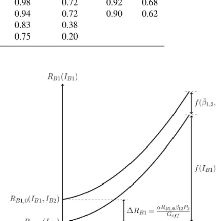
This implies that the resistance of the first element can be increased by a value equivalent to αRB1,0β12P2/Geff com-pared to the reference resistance. The modulation of the re-sistanceRB1is controlled byP2and the effect is illustrated in Fig. 5. The figure also serves to further clarify the differ-ences in the contributions ofTm,1(orP1) andTm,2(orP2). Although not indicated in the figure, the same modulation concept will hold true for the resistance of the second el-ement, RB2(1T2), by applying a control signal to the first element.
4 Results and discussion
The analytically predicted results of the devices are provided in Table 3. However, to verify the validity of the theoreti-cal model and reach a meaningful conclusion, those results need to be compared to results of simulation and experimen-tal methods that extract the coupling coefficients. As such, the simulation and experimental results obtained for the two
Figure 5.Effect on the resistance in terms of the current stimuli. The bottom graph represents the reference curve when biasing the first resistive element alone, while the top graph shows the addi-tional increased resistance when the second resistor is also biased.
thermally coupled MEMS devices are presented next for both vacuum and atmospheric pressure conditions.
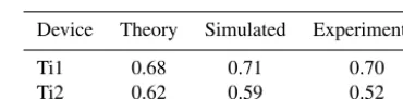
Device Theorya Theoryb Simulated Experimental (µW K−1) (µW K−1) (µW K−1) (µW K−1) Ti1 41.90 58.89 54.33 24.65 Ti2 51.48 41.62 29.55 20.81 aCalculated using the standard approach with Eq. (2) and Eq. (4).bCalculation includes the effect of Eq. (3).
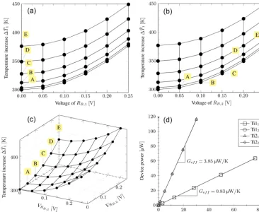
0 to 0.25 V, whileRB2remains unbiased. This offers a bench-mark result similar to what is measured for conventional mi-crobolometers. Once the benchmark curve is obtained, the potential applied across RB2 is increased in 0.05 V incre-ments up to 0.25 V. These increincre-ments are indicated with la-bels A through E in Fig. 6. At each increment, the original potential sweep applied toRB1is repeated. The average tem-peratures of the thin-film Ti resistors are extracted at each point of the multivariable sweep, with the results for the first element plotted in Fig. 6c. These results are also used to ex-tract the electrical power dissipated by the device. These are combined as theP–T curve illustrated in Fig. 6d that serves to extract the beam thermal conductances from the slopes. Note that these are intermediate results. Therefore, only the results of Ti1 under vacuum conditions are presented for brevity. The same method is followed for atmospheric pres-sure conditions and repeated for device Ti2 under both con-ditions.
4.2 Measurement results of the thin-film metal devices The V–I curves are useful to calculate the power dissipa-tion of the devices, sinceGeffis extracted from this. TheR– I curves also provide additional graphical insight into the resistive modulation effect. The next results show the ex-perimental measurements of both devices in Fig. 7a. The sensed element voltage is measured when applying an in-put current sweep under vacuum conditions with the Hewlett Packard 4155B parameter analyser. The input current IB1 is swept up to 500 µA for the devices within the evacuated dewar as long as a maximum power consumption limit of 100 µW is met. The lower curves serve as the reference since
IB2,0=0 µA. Once the reference curves have been obtained, the experiment is repeated at increments of approximately
IB2,i=50 µA and IB2,i=62.5 µA respectively for devices
Ti1 0.68 0.71 0.70
Ti2 0.62 0.59 0.52
Ti1 and Ti2. A very high thermal increase is possible even at moderate power consumption levels for Ti1 because of the low beam thermal conductance. This explains the need to limit the power consumption of the experiment. The slope of the curves suggests a positive TCR as expected for metal devices. The 1/R–I2 curves are also indicated and used to extract the effective thermal conductance using Eq. (20). The results are plotted in Fig. 7b.
4.3 Comparison and discussion of the results
A comparison of the effective thermal conductances for the devices is provided in Table 4. The theoretically derived val-ues using both Eqs. (2) and (3) are compared to the sim-ulation results extracted from Fig. 6d and the experimen-tal results extracted from Fig. 7b. The results compare very well overall, but the experimentally obtained value for Ti2 is slightly smaller than anticipated. This is due to mask align-ment difficulties encountered during manufacturing, as seen in the SEM micrograph in Fig. 4b. This led to the left support beams playing a smaller role in the thermal isolation of the membrane than expected. We do notice a large discrepancy between the analytic and simulated results for device Ti2 at atmospheric pressure conditions. This warranted a deeper in-vestigation into the particular design. It revealed that the en-tire plate of the simulated device does not reach the average temperature of the heater, which meansAeffis much smaller than the value used in the prediction. This leads to a smaller simulated thermal conductance. This is similar to an effect we first observed in conventional microbolometer designs (Schoeman and du Plessis, 2016). Also notice that the ex-perimental values are smaller than those simulated. The sim-ulation is set up withdλ=2 µm. However, microscopic
in-spection revealed that the devices are bending upwards. This was confirmed by a profilometric analysis, and it was found that Ti1 is bending upwards withdλ in excess of 3 µm and
Ti2, with its shorter supports, measuringdλ=2.8 µm. This
Figure 6.Simulation results of the thermoelectric interaction that exists for the Ti devices under vacuum conditions.(a)XZ projection of the thermal profile of RB1for Ti1.(b)YZ projection of the thermal profile ofRB1 for Ti1.(c)3-D thermal profile ofRB1for Ti1. (d)Temperature curves at different power levels to extract the beam thermal conductance.
Figure 7.Experimental results of a parametric current sweep un-der vacuum conditions for the Ti thin-film devices indicating the resulting resistance of the first resistive element,RB1, whileRB2is
biased at different values as indicated in the legend entries. These results are also used to extract the beam thermal conductance. Note that the legends of(b)also apply to(a)but that Ti1 is presented at the top of(a)and at the bottom of(b), as expected when comparing Rto 1/R.(a)ExperimentalR–Icurves.(b)Experimental 1/R–I2 curves.
We use the methods of Sect. 3.1 and Sect. 3.2 to determine the thermal linkage between the resistive elements. Three biasing points, [0, 20, 100] % of the maximumIB1, are se-lected on each of theIB2,2–4curves plotted in Fig. 7a. This results in nine data points for each device. We can use each result to extract a thermal coupling coefficient with Eq. (22) at that biasing point. The nine results are then averaged. The analytic, simulation, and experimental results obtained un-der vacuum conditions are presented in Table 6, while the same results at atmospheric pressure are presented in Table 7. As can be seen from the tabulated average thermal coupling coefficients, the predicted results of the Ti thin-film devices compare very well with the simulation and experimental re-sults. The largest observed errors relative to the developed model are 7.6 % and 16.1 % respectively for the simulation and experimental results.
5 Conclusions
fect. The main reason for the success of the model lies in the definition of Eq. (17). The best results are achieved and per-formance is optimised for coupling over very long lengths of resistors while maintaining a very small separation dis-tance between them. This is typically achieved with long and narrow resistors, or LRWR, and hence, thin-film
resis-tive materials are very suitable. Ti-based devices, for exam-ple, are ideal and outperform alternative material choices like VOx from our experience. We conclude that the developed
model offers a reasonable output that will prove very useful in future MEMS designs of applications making use of ther-mal coupling. Other than the applications mentioned in the introduction, this effect holds potential in the low-frequency domain for solutions of MEMS-based on-chip electrothermal isolators and even signal processing. Designers using alterna-tive design simulation methods, for example at a circuit level using SPICE to simulate ETC, also stand to benefit from the proposed analytic model, since it allows for a simple method to calculate the thermal linkage between elements without the need to use expensive device-level FEM software. This will be the focus of future work. Even our best thermal link-age results of approximately 90 % and 70 %, depending on the pressure conditions, are far from 100 %. As such, design-ers should be cautious to assume ideal thermal linkage, which is often assumed in previous work, and consider incorporat-ing thermal couplincorporat-ing coefficients into their ETC designs.
Data availability. The underlying simulation and measurement data are not publicly available and can be requested from the au-thors if required.
Author contributions. MdP initiated the work by acquiring fund-ing that facilitated the necessary resources and software for design, simulation, and prototyping, offered invaluable insight during dis-cussions, and supervised the work. JS developed the theoretical models, implemented the simulation models, developed and con-ducted the experimental work, carried out data processing and anal-ysis, and drafted the manuscript.
Competing interests. The authors declare that they have no con-flict of interest.
References
Akula, A., Ghosh, R., Sardana, H., Predeep, P., Thakur, M., and Varma, M. R.: Thermal Imaging And Its Application In Defence Systems, in: AIP Conference Proceedings-American Institute of Physics, 1391, p. 333, 2011.
Arndt, M.: Micromachined thermal conductivity hydrogen detector for automotive applications, in: Proceedings of IEEE Sensors, 2, 1571–1575, https://doi.org/10.1109/ICSENS.2002.1037357, 2002.
Baltes, H., Paul, O., and Brand, O.: Micromachined ther-mally based CMOS microsensors, P. IEEE, 86, 1660–1678, https://doi.org/10.1109/5.704271, 1998.
Barritault, P., Brun, M., Lartigue, O., Willemin, J., Ouvrier-Buffet, J.-L., Pocas, S., and Nicoletti, S.: Low power CO2 NDIR sensing using a micro-bolometer detector and a micro-hotplate IR-source, Sensor. Actuat. B, 182, 565–570, https://doi.org/10.1016/j.snb.2013.03.048, 2013.
Castaldo, R., Franck, C. C., and Smith, A. B.: Evaluation of FLIR/IR camera technology for airport surface surveil-lance, in: Enhanced and Synthetic Vision, 2736, 64–74, https://doi.org/10.1117/12.241047, 1996.
Chow, J. and Lai, Y.: Displacement sensing of a
micro-electro-thermal actuator using a monolithically
inte-grated thermal sensor, Sensor. Actuat. A, 150, 137–143, https://doi.org/10.1016/j.sna.2008.11.014, 2009.
Corsi, C., Dundee, A., Laurenzi, P., Liberatore, N., Luciani, D., Mengali, S., Mercuri, A., Pifferi, A., Simeoni, Mirko Tosone, G., Viola, R., and Zintu, D.: Chemical Warfare Agents Ana-lyzer Based on Low Cost, Room Temperature, and Infrared Mi-crobolometer Smart Sensors, Advances in Optical Technologies, 808541, https://doi.org/10.1155/2012/808541, 2012.
Dulski, R., Bareła, J., Trzaskawka, P., and Pia¸tkowski, T.: Applica-tion of infrared uncooled cameras in surveillance systems, in: Electro-Optical and Infrared Systems: Technology and Appli-cations X, 8896, 315–322, https://doi.org/10.1117/12.2028507, 2013.
Elmi, I., Zampolli, S., Cozzani, E., Mancarella, F., and Car-dinali, G.: Development of ultra-low-power consumption {MOX} sensors with ppb-level VOC detection capabilities for emerging applications, Sensor. Actuat. B, 135, 342–351, https://doi.org/10.1016/j.snb.2008.09.002, 2008.
Galeazzi, M. and McCammon, D.: Microcalorimeter and bolometer model, J. of Appl. Phys., 93, 4856–4869, 2003.
Gray, P. R. and Hamilton, D. J.: Analysis of Electrother-mal Integrated Circuits, IEEE J.Solid-St. Circ., 6, 8–14, https://doi.org/10.1109/JSSC.1971.1050152, 1971.
Huang, Q.-A. and Lee, N. K. S.: Analysis and design of polysili-con thermal flexure actuator, J. Micromech. Microeng., 9, 64–70, https://doi.org/10.1088/0960-1317/9/1/308, 1999.
Johnson, R. and Higashi, R.: A highly sensitive silicon chip micro-transducer for air flow and differential pressure sensing applica-tions, Sensor. Actuat., 11, 63–72, https://doi.org/10.1016/0250-6874(87)85005-9, 1987.
Khan, U. and Falconi, C.: Temperature distribution in membrane-type micro-hot-plates with circular geometry, Sensor. Actuat. B, 177, 535–542, 2013.
Kim, G. and Ko, H.: Behavioral modeling and experimental vali-dation of uncooled microbolometer, in: 2015 IEEE SENSORS, 1–3, https://doi.org/10.1109/ICSENS.2015.7370392, 2015. Kiran, S. and Karunasiri, G.: Electro-thermal modelling of infrared
microemitters using PSPICE, Sensor. Actuat. A, 72, 110–114, https://doi.org/10.1016/S0924-4247(98)00215-5, 1999. Klaassen, E. H., Reay, R. J., and Kovacs, G. T. A.:
Diode-based Thermal RMS Converter With On-chip Circuitry Fab-ricated Using Standard CMOS Technology, in: Solid-State Sensors and Actuators, 1995 and Eurosensors IX. Transduc-ers ’95. The 8th International Conference on, 1, 154–157, https://doi.org/10.1109/SENSOR.1995.717119, 1995.
Kokkas, A. G.: Thermal analysis of multiple-layer structures, IEEE T. Electron Dev., 21, 674–681, https://doi.org/10.1109/T-ED.1974.17993, 1974.
Liddiard, K. C.: Application of mosaic pixel microbolome-ter technology to very high-performance, low-cost
ther-mography and pedestrian detection, in: Infrared
Tech-nology and Applications XXXIX, 8704, 8704, 980–988, https://doi.org/10.1117/12.2018593, 2013.
Louw, W. J., Hamilton, D. J., and Kerwin, W. J.:
Inductor-less, capacitor-less state-variable
electrother-mal filters, IEEE J. Solid-St. Circ., 12, 416–424,
https://doi.org/10.1109/JSSC.1977.1050923, 1977.
Mankame, N. D. and Ananthasuresh, G. K.: Comprehensive thermal modelling and characterization of an electro-thermal-compliant microactuator, J. Micromech. Microeng., 11, 452– 462, https://doi.org/10.1088/0960-1317/11/5/303, 2001. Matzen, W. T., Meadows, R. A., Merryman, J. D., and
Emmons, S. P.: Thermal techniques as applied to
functional electronic blocks, P. IEEE, 52, 1496–1501,
https://doi.org/10.1109/PROC.1964.3438, 1964.
Nazdrowicz, J., Szermer, M., Maj, C., Zabierowski, W., and Napieralski, A.: A study on microbolometer electro-thermal cir-cuit modelling, in: 2015 22nd International Conference Mixed Design of Integrated Circuits Systems (MIXDES), 458–463, https://doi.org/10.1109/MIXDES.2015.7208563, 2015. Niklaus, F., Jansson, C., Decharat, A., Källhammer, J.-E.,
Petters-son, H., and Stemme, G.: Uncooled infrared bolometer arrays operating in a low to medium vacuum atmosphere: performance model and tradeoffs, in: Defense and Security Symposium, In-ternational Society for Optics and Photonics, 65421M–65421M, 2007.
Sberveglieri, G., Hellmich, W., and Müller, G.: Silicon hotplates for metal oxide gas sensor elements, Microsyst. Technol., 3, 183– 190, https://doi.org/10.1007/s005420050078, 1997.
Schoeman, J. and du Plessis, M.: Characterisation of the Electri-cal Response of a Novel Dual Element Thermistor for Low Fre-quency Applications, SAIEE Africa Research Journal, 103, 9– 13, https://doi.org/10.23919/SAIEE.2012.8531972, 2012. Schoeman, J. and du Plessis, M.: An analytic model employing an
elliptical surface area to determine the gaseous thermal conduc-tance of uncooled VOx microbolometers, Sensor. Actuat. A, 250, 229–236, https://doi.org/10.1016/j.sna.2016.09.033, 2016. Senesac, L. R., Yi, D., Greve, A., Hales, J. H., Davis, Z. J.,
Nichol-son, D. M., Boisen, A., and Thundat, T.: Micro-differential thermal analysis detection of adsorbed explosive molecules us-ing microfabricated bridges, Rev. Sci. Instrum., 80, 035102, https://doi.org/10.1063/1.3090881, 2009.
Shie, J.-S., Chen, Y.-M., Ou-Yang, M., and Chou, B. C. S.: Charac-terization and Modeling of Metal-Film Microbolometer, Journal of Mircoelectromechanical Systems, 5, 298–306, 1996. Simon, I., Bârsan, N., Bauer, M., and Weimar, U.:
Micro-machined metal oxide gas sensors: opportunities to im-prove sensor performance, Sensor. Actuat. B, 73, 1–26, https://doi.org/10.1016/S0925-4005(00)00639-0, 2001. Sisto, M. M., Garcia-Blanco, S., Le Noc, L., Tremblay, B.,
Desroches, Y., Caron, J.-S., Provencal, F., and Picard, F.: Pres-sure sensing in vacuum hermetic micropackaging for MOEMS-MEMS, J. Micro-Nanolith., MEM., 9, 041109–041109, 2010. Topaloglu, N., Nieva, P., Yavuz, M., and Huissoon, J.: A Novel
Method for Estimating the Thermal Conductance of Un-cooled Microbolometer Pixels, in: IEEE International Sym-posium on Industrial Electronics, ISIE 2007, 1554–1558, https://doi.org/10.1109/ISIE.2007.4374834, 2007.
Topaloglu, N., Nieva, P. M., Yavuz, M., and Huissoon, J. P.: Modeling of thermal conductance in an uncooled microbolometer pixel, Sensor. Actuat. A, 157, 235–245, https://doi.org/10.1016/j.sna.2009.11.018, 2010.
von Arx, M., Paul, O., and Baltes, H.: Process-dependent thin-film thermal conductivities for thermal CMOS MEMS, J. Micro-electromech. S., 9, 136–145, https://doi.org/10.1109/84.825788, 2000.
Yan, D., Khajepour, A., and Mansour, R.: Design and model-ing of a MEMS bidirectional vertical thermal actuator, J. Mi-cromech. Microeng., 14, 841–850, https://doi.org/10.1088/0960-1317/14/7/002, 2004.
Yoon, E. and Wise, K. D.: A wideband monolithic RMS-DC con-verter using micromachined diaphragm structures, IEEE T. Elec-tron Dev., 41, 1666–1668, https://doi.org/10.1109/16.310122, 1994.