Soft–Switched Interleaved Boost Converter with
Quadratic Voltage Gain for Renewable Energy
Applications
João Dallamuta, Marcelo Fiori, Mikael Oliveira, Aziz Demian and Lúcio R. Barbosa
Universidade Estadual de Londrina, Londrina – Paraná, Brazil e-mail: lbarbosa@uel.br
Abstract– An efficient soft switching interleaved boost converter with quadratic voltage gain is presented. Two boost-quadratic-topology switching cells are interleaved to minimize EMI while operating at lower switching frequency and soft switching to minimize losses. The result is a system with high conversion efficiency, able to operate in a pulse-width-modulation (PWM) way. Seven transition states of the soft switching converter in one switching period are described. In order to illustrate the operational principle key implementation details, including simulations, are described. The validity of this converter is guaranteed by the obtained results.
Index Term
–
Interleaved, Quadratic, Soft-Switched,.I. INTRODUCTION
The demand of efficient step-up dc-dc converters has been rising due to the increase of battery powered applications and low voltage storage elements. Typical applications are embedded systems, renewable energy systems, fuel cells, mobility applications and uninterrupted power supply (UPS) [1], [2] and [3]. These applications demand high step-up static gain, high efficiency and reduced weight, volume and cost.
Buck, boost, buck-boost, cuk, sepic and zeta are the basic single-switch topologies that can be used in non-isolated, high frequency, switch-mode power converters. They are used mainly in dc-dc converters [4], but sometimes in ac-dc converters, and are effective in converting the supplied input voltage to the required output voltage. There are, however, applications where none of the basic converter topologies are suitable and alternative topologies need to be considered.
Topologies with different values of voltage gain ((G) can be produced if basic converters are cascaded with each other. It is an attractive solution for extreme voltage gain applications [5], [6]. Nevertheless, it is complex and the cost is high because two sets of power devices, magnetic cores and control circuits are required. The system stability with cascade structure is a big issue and the control circuit should be designed carefully [7], [8]. The rectifier reverse-recovery problem is serious in the high voltage side because a high voltage level should be sustained for the rectifier used in the high voltage side [9]. Therefore, the efficiency is not high and the electromagnetic interference (EMI) noise problem is serious.
It was shown in [10] that such cascaded converters can be implemented with only a single switch and thus single switch converters with non-standard conversion ratios can be synthesized. These converters are frequently referred to as quadratic converters as G(D) is related to the square of D (duty cycle).
How to avoid the extreme duty cycle and how to minimize the current ripple are the major considerations in these applications. In order to minimize the current ripple, reduce the passive component size; improve the transient response and increase the power level, the interleaved structure is applied in many large current and high power density applications.
The concept of interleaving several switching cells is not new, and was originally used as a method for overcoming the limitations of ordinary power conversion techniques and device technologies [11]. Recognition of the general merits of interleaved conversion has prompted a diverse variety of subsequent investigations, as reflected in the literature.
A number of quadratic converters have been proposed in the power electronics literature [12-15]. In order to maintain high switching frequency operation while maximizing the converter efficiency, soft switching cells are introduced to the converters.
Most recent development in high frequency converter configuration is a hybrid of resonant soft switching and pulse-width-modulation (PWM) control. This group of converters is called soft switching PWM converters, an example of these converters are presented in [16]. In the soft switching PWM converters, the switches operate in resonant mode only during switching transitions and then, return to PWM operation for the rest of a switching period.
A comparison of soft switching methods for PWM converters had shown that passive method has better efficiency in the high power operation region, while active method outperforms the passive method in the low power regions [17]. However, this small improvement in efficiency is partially countered by higher gate drive losses, higher control complexity, and lower reliability compared to the passive method.
quadratic boost converter[18] shown in Fig. 1, combined with the soft switching technique to lower the switching losses in the approach proposed in [19-21], can reduce the net ripple amplitude and raises the effective ripple frequency of the overall converter without increasing switching losses.
Fig. 1. Quadratic Boost Topology.
The main goal of this system can therefore realize a savings in filtration and energy storage requirements, resulting in greatly improved power conversion densities without sacrificing efficiency.
The features of the proposed converter are discussed in this paper and the principle of operation, simulation and experimental results are presented to validate the proposed solution.
II. PROPOSED STRUCTURE
A. Circuit Description
A configuration of the proposed structure is shown in Fig. 2. This quadratic converter is based on the interleaved Boost converter, integrated with the proposed soft switching auxiliary circuit. The quadratic boost converter with a single
active switch is shown in Fig. 1 where Vi is the input voltage,
Vo the output voltage and D the nominal duty ratio. This
converter contains two LC filters, one active switch and three passive switches. This converter uses only one control circuit instead of two control circuits required when two basic boost converters are connected in cascade. In this converter, the DC voltage gain is a quadratic function of the nominal duty ratio
D, i.e., Vo/Vi = 1/(1-D)2.
As the proposed structure is derived from the quadratic boost converter, there are two filter inductors for each stage connected in parallel. The input current ripple is reduced by the parallel stages operating with different phases. The diodes
DA1 and DA2 are the output diodes and operate like the output
diodes of the interleaved boost converter. The output filter and
load are represented by Co and Ro.
The steady-state operating conditions in continuous conduction mode can be derived from the ON and OFF operating conditions of the active switch and diodes. Continuous conduction mode assumes that the peak inductor current ripple is smaller than the DC component of the inductor current; therefore, the total current is always positive. When all losses are neglected, the steady-state operating conditions [19] are given by:
)] 1 ( / [
1 V D
VC i (1)
] ) 1 ( /
[V D 2
Vo i (2)
D
RV ILB1 i 4
1
(3)
D
RV
I i
LB2 3
1
(4)
Fig. 2. Proposed Interleaved Boost Converter.
However, the above equations change when interleaving technique is applied as:
D
RV I
I i
LB LB
2
1 4
3 1
(5)
D
RV I
I i
LB LB
2
1 3
4 2
(6)
The benefits of interleaving can be understood intuitively using a simple graphical analysis to show how the output power is shared between two boost switching cells connected in parallel.
For simultaneous synchronous operation (wherein the commutation instances of the two controlled switches are identical), the circuit performance is equivalent to a single boost converter with equal total energy storage and equal total semiconductor die area. The inductor and diode ripple current waveforms that result are shown in Fig. 3 as solid ones.
If these same converter cells are interleaved, such that the commutation instances of the second switch are delayed relative to those of the first switch by half a switching period,
the resultant ripple waveforms are those shown asdashed lines
in Fig. 3. Compared to the non-interleaved case with equal
energy storage, the interleaved ripple waveforms have smaller amplitudes and increased frequencies, reducing the filtration requirements, as in [19].
In order to simplify the description and the explanation of
the proposed converter, filter inductance’s LB1, LB2, LB3 and
sources. The voltage across Co present no ripple, all
components are treated as being ideal, and the input current
flows through freewheeling diodes DA1 and DA2 until switch
S1 or S2 are turned on at time to. According to its working
cycle, operations modes are described as follows.
Fig. 3. Dual boost converter ripple waveforms.
B. Topological States and Mathematical Analysis
The operation of the circuit will be described considering
the branch 1(S1), since the branch 2 (S2) operates in the same
way. Based on these assumptions, circuit operations in one switching cycle can be divided into ten stages. The ten dynamic equivalent circuits of the new converter during one
switching period is shown in Fig. 4 where the main switch S1
Fig. 4. Topology modes.
In this section, the analytical expressions describing the operation of the proposed converter are presented. The following definitions are assumed
R R o 1/ L C
(7) R R o LB C L V I 2 1 (8) R R C LB C L V I 1 1 2 (9) 1 1 Vo/VC
G (10)
i
C V
V
G2 1/ (11)
i
o V
V
G / (12)
The resonant components are assumed to be with the same
values: LR1=LR2=LR3=LR and CR1=CR2=CR.
1) First Mode – [t0, t1], Fig. 4(a): Before t=t0, the main
switch S1 maintains turn-off state, the current ILB1 flows
through DB1 and ILB2 through DA1. This stage begins when S1
turns on with ZCS at t=t0. The resonant inductor LR1
discharges linearly due to output voltage Vo from ILB2 + ILB4 to
ILB4. The stage ends when diode DA1 turns off at t=t1. The
resonant iLR1(t), iLR2(t) and vCR1(t) can be respectively
described as: t L V I I t
iLR1() LB2 LB4( o/ R) (13)
o
CR t V
v 1() (14)
0 ) (
2 t
iLR (15)
o
t11/
(16)
2) Second Mode – [t1, t2], Fig. 4(b): In this stage, the
resonance begins when DR1 turns on at t=t1’. The resonant
route proceeds by way of LR1, CR1, S1 and DR1. The resonant
current iLR1(t) decreases and the resonant voltage vCR1(t) also
decreases via the resonance of LR1 and CR1. The resonant
inductor LR2 charges linearly from zero to ILB1. This state ends
when the voltage vCR1(t) reaches capacitor C1 voltage VC1 at
t=t2. The resonant iLR1(t) and vCR1(t) can be respectively
described as:
t L V t
iLR2()( C1/ R) (17)
o
t
t´2()2/
(18) t L C V I t i o R R o LB
LR1() 4 sin( ) (19)
) cos( )
(
1 t V t
vCR o o (20)
o o C V V t
cos 1( 1/ ) 2
(21)
At the end of this stage iLr1is equal to:
2 1 1 2 4 2 1 1 1 ) ( G I I t i LB LB
LR (22)
3) Third Mode – [t2, t3], Fig. 4(c): In this mode iLR1(t)
becomes ILB4 due to capacitor voltage VC1. The expression for
iLR1(t) and vCR1(t) are:
2 1 1 2 4 1 1 1 1 ) ( G I I t L V t i LB LB R C
LR (23)
1
1() C
CR t V
v (24)
o o C V V t
cos 1( 1/ ) 3
(25)
4) Fourth Mode – [t3, t4], Fig. 4(d): The main switch is
conducting and the currents ILB1 and ILB2 flow through the
power switch. All branch 1 diodes are blocked and the
inductors LB1 and LB2 store energy. The equations that
describe this mode are:
4
1() LB
LR t I
i (26)
1
1() C
CR t V
v (27)
4 5
4 t t
t
(28)
5) Fifth Mode – [t4, t5], Fig. 4(e): At the instant t4, switch
S1 is turned-off in a ZVS way and the energy stored in the
CR1 through the diode DR2. In this time interval, CR1 linearly
charges to zero voltage. The resonant iLR1(t), iLr2(t) and vCR1(t)
can be respectively described as:
4
1() LB
LR t I
i (29)
1
2() LB
LR t I
i (30)
t C I I V t
vCR1() C1[( LB1 LB2)/ R] (31)
) /(
1 2 1 1
5 G
t oo
(32)
6) Sixth Mode – [t5, t6], Fig. 4(f): In this stage, the
resonance begins when DB1 turns on at t=t5. The resonant
route proceeds by way of LR2, CR1, DR1, DB2 and DB1. The
resonant current iLR2(t) decreases and the resonant voltage
vCR1(t) increases. This state ends when the current iLR2(t)
reaches zero at t=t6. The resonant iLR2(t) and vCR1(t) can be
respectively described as:
) cos( )
( 1
2 t I t
iLR LB o (33)
t C L I t v o R R LB
CR1() 1 sin( ) (34)
) 2 /(
6 o
t
(35)
7) Seventh Mode – [t6, t7], Fig. 4(g): At the instant t7,
switch DB2 is turned-off and the energy stored in the inductor
LB2 is transferred to the resonant capacitor CR1 through the
diode DR2. In this time interval, CR1 linearly discharges to Vo
-VC1. The resonant capacitor voltage vCR1(t) can be described
as:
0 ) (
2 t
iLR (36)
t C I V t
vCR1()2 C1( LB2/ R) (37)
) /(
) 1
( 1 2 1 1
7 G G
t o
(38)
8) Eighth Mode – [t7, t8], Fig. 4(h): In this stage, the
resonance begins when DA1 turns on at t=t7. The resonant
route proceeds by way of LR1, C1, DR2, CR1, DA1 and Co. The
resonant current iLR1(t) increases and the resonant voltage
vCR1(t) also increases via the resonance of LR1 and CR1. This
state ends when the voltage vCR1(t) reaches output voltage Vo
at t=t8. The resonant iLR1(t) and vCR1(t) can be respectively
described as: )) cos( 1 ( )
( 4 2
1 t I I t
iLR LB LB o (39)
) sin( )
( 1 2
1 t C L I V V t v o R R LB C o
CR (40)
1 1 1 8 1 sin 1 G t o (41)
At the end of this stage, iLR1is equal to:
1 1 2 4 8 1 1 1 1 ) ( G I I t
iLR LB LLB
(42)
9) Ninth Mode – [t8, t9], Fig. 4(i): When capacitor CR1
voltage becomes Vo diode DR1 is turned on and LR1 current
increases linearly. This stage finishes when the LR1 current
becomes equal to ILB2 +ILB4.
t L V t i t i R C LR LR 1 8 1
1() ( ) (43)
1 ) ( 1 2 1 1
9
t G
o
(44)
10) Tenth Mode – [t9, t0], Fig. 4(j): During this stage
transference of energy from source to load occurs through
diode DA1, starting another switching cycle.
4 2
1( ) LB LB
LR t I I
i (45)
o
CR t V
v 1() (46)
0 ) (
2 t
iLR (47)
B. Main Waveforms and Static Gain
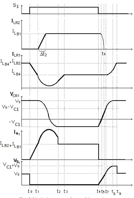
Fig. 5. Ideal relevant waveforms of the topology.
The static gain, which represents the ratio between the output and the input voltages as function of the duty cycle, can be obtained by analyzing the voltage waveforms of the
inductor LB1 and/or LB2 observing the time intervals.
After the mathematical analyses, the expression of the static gain can be obtained:
) 1 ( 2 1 1 1 / 1 1 2 2 1 2 G T D V V G o s i C (48) ) 1 ( 2 1 1 1 / 1 1 2 2 1 2 G T D V V G o s i C (49) 2 1
/V GG
V
G o i (50)
where:
S - the switching period.
The expression of the static gain is illustrated in Fig. 6. According to the expressions, it appears clearly that total static
gain G (Fig. 8, when α1=α2=α) is always higher compared to
the conventional boost converter. Thus, it seems more appropriate to develop the new quadratic converter, which has high conversion ratio in a large range of duty cycle.
Fig. 6. Static gain curves.
III. DESIGN PROCEDURE
Design of conventional quadratic and interleaved PWM converters have been well presented in literatures. Thus, it is more significant to focus on design procedures of the auxiliary circuit [20]. The resonant inductors and resonant capacitor are the most important components when designing the auxiliary circuit. The proposed auxiliary resonant circuit provides soft-switching conditions for the main switch. The following design procedure is developed considering procedures such as those presented previously in [12-16].
Snubber inductor LR1 is selected to allow its current
decreases from the maximum current (ILB2+ILB4) to ILB4 within
tr time periods, during the turn-on of the main switch. In this
case, from (13), it can be written:
r LB o
R V I t
L1( / 2max) (51)
Snubber inductor LR2 is selected to permit its current to rise
up to at most the maximum input current within tr time
periods, during the turn-on of the main switch. In this case, from (17), it can be written:
r LB C
R V I t
L2 ( 1/ 1max) (52)
where:
tr - the switching period.
Theses equations provide ZCS turn-on for the transistor.
Snubber capacitor Cr is selected to be discharged from VC1
to zero with the maximum LB1 and LB2 currents over at least
the time period tf during the turn-off of the transistor. For this
state, according to (25) it is obttained
r C LB
LB
R I I V t
C [( 1max 2max)/ 1] (53)
where:
tf - the fall time of the transistor.
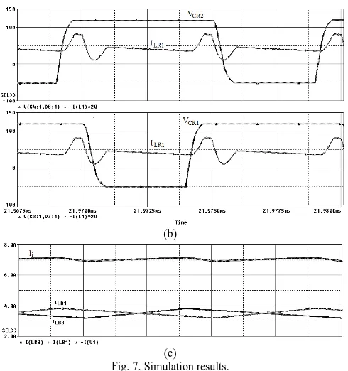
IV. SIMULATION AND EXPERIMENTAL RESULTS The converter was simulated using simulation software
ORCAD®. Figure 7 (a-d) shows the simulation results of the
experimental waveforms obtained in laboratory are shown
from Fig. 8 (a-d) and were acquired using a THS720
Tektronix® oscilloscope and a Tm 502A Tektronix® current
gauge The newly proposed converter operates with an input
voltage Vi=50V, output voltage Vo=150V, output power of
400W and a switching frequency of 100KHz. The major parameters and components are given in Table I.
TABLE I
Components Used in the Proposed Converter
Parameters
Component Simulation Experimental
Main switches (S1 and S2) Ideal SK 60 GAL 125
Diodes Ideal APT 30D100B
Resonant inductor (LR1) 15 µH 15 µH Resonant inductors (LR2 and LR3) 3.5 µH 3.5 µH Resonant capacitors (CR1 and CR2) 20.4 nF 20.4 nF Filter inductors (LB1 and LB3) 450 µH 450 µH Filter inductors (LB2 and LB4) 545 µH 545 µH Filter capacitor C1and C2 330 µF 330 µF Output capacitor Co 330 µF 330 µF
It is noted from Figures 7(a) and 8(a) that the main switches are turned on under ZCS. The main switches take the load current and the charging current of the resonant capacitor. The resonant capacitor starts to transfer its stored energy to
resonant inductor LR1 during the turn-on period of main
switch. The converter has not exceeded the voltage limits; however, the current stress is slightly higher for a very short period. The main switches also turn off under ZVS. The current and voltage wave shapes are similar to theoretical waveforms.
(a)
(b)
(c)
Fig. 7. Simulation results.
It can be seen in Figures 7(b) and 8(b) that after switches
are turned off under ZVS; capacitors CR1 and CR2 are charged.
As soon resonant capacitors reach (Vo-Vc1), the resonance
starts between resonant capacitors and LR1. Figures 7(c) and
8(c) shows the currents in the two input inductors, LB1 and
LB3. In this figure can be verified the delay of half operation
period among the command of these devices. This delay is responsible by minimization of the input current ripple.
(b)
(c)
Fig. 8. Experimental results.
Fig. 9 shows the current in filter inductor LB1 and input
current Ii. The small oscillation is due to the inductance value.
Fig. 9. Current in filter inductor ILB1 and input current Ii.
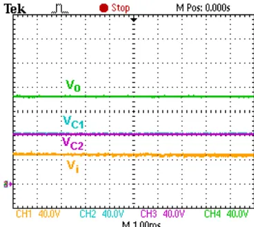
Fig. 10 shows the voltage step up obtained with the proposed circuit. As expected, one can see that input voltage increases in the converter.
The efficiency of the power circuit reached at nominal load is equal to 88%, as shown in Fig. 11. These values were
obtained using a Yokogawa® WT230 Digital Power Meter. To
provide a comparative analysis about the efficiency levels achieved with the laboratory prototype, a converter without the proposed soft-commutation cell was also built in the laboratory using the same layout and the same components. Thus, in this situation, one can conclude that significant efficiency improvements can be achieved with the application of the proposed soft commutation cell.
Fig. 10. Output voltage (Vo) and capacitors voltage (VC1 and VC2).
Fig. 11. Curve of efficiency versus output power.
IV. CONCLUSIONS
The use of interleaving permits the reduction of conduction losses in the switches, maintaining a good quality of the input current, resulting in higher conversion efficiency compared to non-interleaved quadratic converters. A method for combining interleaved and quadratic converters to predict ripple amplitudes has been demonstrated and applied as a design tool; the use of the auxiliary commutation circuit providing soft switching of the main switches enable optimization of the conversion efficiency.
ACKNOWLEDGMENT
This Project was financed by the CNPq (150627/2010-6 process).
REFERENCES
[1] Q. Zhao and F. Lee, “High-efficiency, high step-up dc-dc converters,”, IEEE Trans. on Power Electron.., vol. 18, nº 1, pp. 65-73, Jan. 2003. [2] R. Wai and R. Duan, “High step-up converter with coupled-inductor”
IEEE Trans. on Power Electron., vol. 20, nº. 5, pp. 1025-1035, Sep. 2005.
[3] R. Wai and R. Duan, “High-efficiency power conversion for low power fuel cell generation system.” IEEE Trans. on Power Electron., vol. 20, pp. 847-856, Jul. 2005.
[4] D. Maksimovic and S. Cuk, “General properties and synthesis of PWM dc-dc converters,” in IEEE Power Electronics Specialists Conference, pp. 515-525, 1989.
[5] L. Huber and M. Jovanovic, “A design approach for server power supplies for networking,” in Proc. IEEE APEC´00, 2000, pp. 1163-1169.
[6] Y. Ren, M. Xu, K. Yao, Y. Meng, and F. Lee, “Two-stage approach for 12-V VR,” IEEE Trans. Power Electron, vol. 19, no 6, pp. 1498-1506, Nov, 2001.
[7] X. Feng, J. Liu, and F. Lee, “Impedance specifications for stable dc distributed power systems,” IEEE Trans. Power Electron., vol.17, no 2, pp. 157-162, Mar. 2002.
[8] C. Wildrick, F. Lee, B. Cho, and B. Choi, “A method of defining the load impedance specification for a stable distributed power system”
IEEE Trans. Power Electron., vol. 10, no 3, pp. 280-285, May 1995.
[9] W. Li and X. He, “A family of interleaved dc-dc converters deduced from a basic cell with winding-cross-coupled inductors (WCCIs) for High step-up or step-down conversions” IEEE Trans. Power Electron.,
vol. 23, no 4, July 2008.
[10] D. Maksimovic and S. Cuk, “Switching converters with wide DC conversion range”, IEEE Transactions on Power Electronics, vol. 6, no. 1, pp. 151-157, Jan. 1991.
[11] D. Garth, W. Muldoon, G. Benson, and E. Costague, “Multi-phase, 2 Kilowatt, High Voltage, Regulated Power Supply”, IEEE Power
Conditioning Specialists Conference Record, pp. 110-116, 1971.
[12] L. Barreto, E. Coelho, V. Farias, L. Freitas, and J. B. Vieira, “A quasi-resonant quadratic boost converter using a single quasi-resonant network,” in
IEEE 2003 Power Electronics Specialists Conference, pp. 595-599,
2003.
[13] L. Barbosa, J. Vieira, L. Freitas, M. Vilela, and V. Farias, “A buck quadratic PWM sof-switching converter using a single active switch,”
IEEE Transactions on Power Electronics, vol. 14, pp. 445-453, May
1999.
[14] V. Pacheco, A. Nascimento, V. Farias, J. Vieira, and L. Freitas, “A quadratic buck converter with lossless commutation,” IEEE
Transactions on Industrial Electronics, vol. 47, pp. 264-272, April 2000.
[15] A. Pereira, L. Barbosa, J. Rossi, and M. Almeida, “A stressless buck quadratic PWM soft-switched converter,” in IEEE International
Telecommunications Energy Conference, pp. 150-155, 2002.
[16] J. Lambert, L. Barbosa, E. Coelho, L. Freitas, J. Vieira, and V. Farias, “A Boost PWM Soft-single-switched converter with low voltage and current stresses,” IEEE Transactions on Power Electronics, vol. 13, no. 1, pp. 16-35, Jan. 1998.
[17] I. Matsuura, K. Smith, and K. Smedley, “A comparison of active and passive soft switching methods for PWM converters,” in IEEE 1998
Power Electronics Specialists Conference, pp. 94-100, 1998.
[18] L. Barbosa, E. Coelho, L. Freitas, J. Vieira, and V. Farias. Analysis of a soft-switched quadratic boost converter. Brazilian Journal of Power Electronics, Campo Grande, v. 18, n.3, p.1047-1054, jun./aug. 2013. [19] L. Barbosa, E. Coelho, L. Freitas, J. Vieira, and V. Farias, “PWM
Soft-Switched Converters with a Single Active Switch” Trans. of IEEJ, Inc.
(Industry Applications society)”, vol. 117-D, no11, pp. 1305-1310,
November 1997.
[20] L. Barbosa, “A zero-voltage-transition interleaved boost converter and its application to pfc” Advances in Power Electronics, vol. 2011, pp. 1-10.