ISSN: 2319-6505
SECURE TAP CONTROLLER IP CORE
Shelja A S
1, Nandakumar R
2and Muruganantham C
31Department of Electronics and Communication Engineering, NCERC 2Engineer, N.I.E.L.I.T, Calicut
3Department of Electronics and Communication Engineering, NCERC
A R T I C L E I N F O A B S T R A C T
The objective of the work is to design and implement a reusable tap IP core in HDL. The standard IEEE 1149.1 popularly known as JTAG is an established technology and industry standard for on-chip boundary scan testing of SoCs. JTAG TAP controllers used as delivery and control mechanism for Design For Test also poses a security threat. The attackers may try to extract details or modify or controls the signals of internal logic using JTAG port as it does not preclude any protection measures. The objective of this work is to design and implement a TAP controller IP core compatible with IEEE 1149.1-2013 revision of the standard. The paper also suggests the use of lightweight cryptographic ciphers to ensure the authenticity of devices in JTAG chain to defend against JTAG attacks. Also it may be used to ensure the communication secrecy between JTAG master and associated devices.
INTRODUCTION
A TAPC is probably the most common part used in support of on-chip testing. With the emergence of IJTAG many SOC design will be using multiple TAPC for accessing internal logic during test. TAPC is a part of the IEEE 1149.1 standard. IEEE 1149.1, the standard for test access port and boundary scan architecture is a common platform for device, board and system level testing. The standard, popularly known as JTAG was originally introduced in the year 1990 and it is now a well established technology in the industry. A TAPC is probably the most common part used in support of on-chip testing. The original motivation for JTAG was boundary scan testing. Boundary scan is a method for gaining direct control of IO pins of a circuit at boundary of chip during test. This enables efficient testing on interconnection between devices that are mounted on a circuit board. The JTAG control is not limited at just the boundary of device it can also be used to gain access to internal structures during the test of device itself. It provides low cost technique for functional, and in- circuit testing that does not requires the test system to have direct access to each node.
The architecture of IEEE 1149.1 boundary scan includes a Test Access Port (TAP) interface, TAP controller (TAPC) logic, Boundary Scan Registers (BSR), Instruction Register (IR) and Test Data Registers (TDR). The IR and TDR form separate scan paths arranged between the Test Data Input (TDI) pin and Test Data Output (TDO) pin. This architecture allows the TAP to select and shift data through one of the path without accessing the other. When the test logic is active only one register is connected between the TDI and TDO interface
depending on the value at Test Mode Select (TMS) signal. TCK is the test clock and is not synchronized with the system clock. A significant advantage of JTAG is that it requires only a minimum set of test access pins as it uses a serial interface. It facilitates design reuse and provides a standard protocol on-chip testing.
But when this standard is used for boundary-Scan chained device is put into test mode where their I/Os are completely under control of the Boundary register content. But when the chained TAPs pass through the TLR state; these instructions are replaced with not test mode instructions. The I/O pins then revert to being connected to the internal device logic which will be in an unknown state. The results of this reconnection are unpredictable [3].
The 2013 revision of the standard consider this issue and suggest an optional controller for avoiding disruptions caused to the device. An attempt is made to study the effect of the new controller to the test logic of the standard.
TAPCONTROLLER
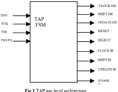
TAP controller is a synchronous machine which provides access to the device under test and controls the behaviour of test logic using its 4-wired interface. It is a 16 state FSM which generates clocks and control signals to the associated test logic. Figure 1 shows the top level architecture of TAPC. Test clock TCK and mode select signal TMS controls the operation of TAPC. An optional TRSTN pin may be used to asynchronously reset the test logic if required and it is active low. A reset of the test logic can also be achieved within five TCKs or less by setting the TMS input high
of Current Advanced
Research
Article History:
Received 18th August, 2016
Received in revised form 2nd
September, 2016 Accepted 27th October, 2016
Published online 28th November, 2016
© Copy Right, Research Alert, 2016, Academic Journals. All rights reserved.
RESEARCH ARTICLE
ISSN: 2319 - 6475
Key words:
IP core; IEEE 1149.1, TAP; JTAG; boundary scan; DFT
International Journal of Current Advanced Research Vol 5, Issue 11, pp 1437-1443, November 2016
The TAPC will be initialized to test logic reset state at the power up. State transitions occur on the rising edge of TCK based on the value of TMS. The FSM has two scan paths for data transmission: one for instruction scan and other for data scan. The state diagram includes six steady states: Test-Logic-Reset, Run-Test/Idle, Shift-DR, Pause-DR, Shift-IR, and Pause-IR. To load and execute a new instruction FSM control is moved to the Select IR-Scan state, from where, it moves through the various states, Capture-IR, Shift-IR, and Update-IR, as required. The last operation is the Update-IR operation and the instruction loaded into the shift section of the Instruction register is latched to the Instruction register to become the new current instruction. This causes the Instruction register to be deselected as the register connected between TDI and TDO and the Data register identified by the new current instruction to be selected as the Data register between TDI and TDO. From now, one can manipulate the data register with the generic signals; Capture-DR, Shift-DR, and Update-DR control signals. TCK can be stopped in either a high or low state without loss of data.
The functional table for the implemented example is given in table 1 with the encoding. The encoding used here is just an example. Different encoding schemes may be used.
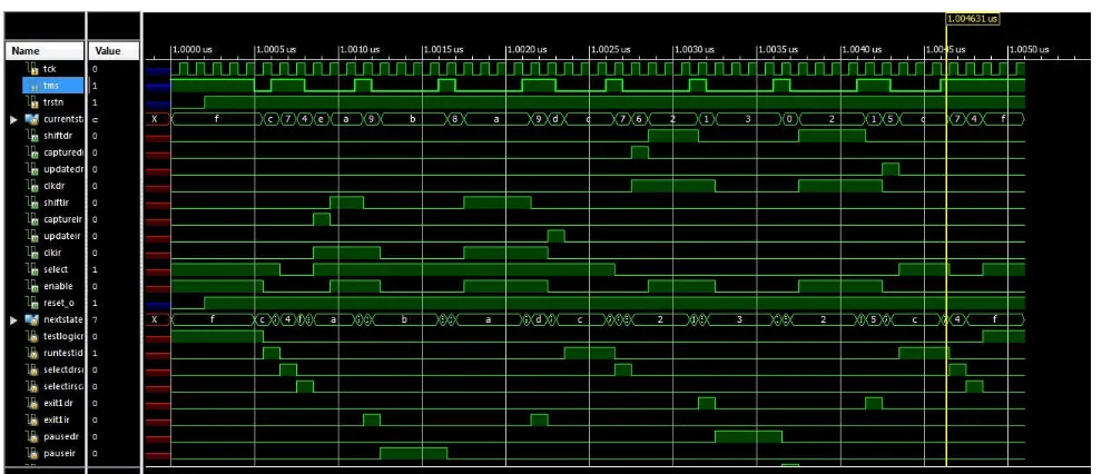
Simulation Results
The design is simulated using Modelsim simulator and the waveform obtained is shown in figure 2. The state transition and output signals of TAPC can be verified by applying the following exhaustive test pattern to the TMS input:
1011000100010000110001000010001000110011
IEEE1149.1-2013REVISION
Since the last revision of the standard in 2001, the industry witnessed a drastic change in the IC technology. Many of these changes have been driven by design complexity and there are many devices available with programmable features including programmable IO behaviour [4]. Boundary scan testing put the device IOs in to test mode were their IOs are controlled by boundary register contents. The standard uses instructions like EXTEST and CLAMP for this. When the non-test instructions like BYPASS or IDCODE is encountered between the test mode instruction the TAP pass through TLR state and IO pins are revert back to functional mode [4]. These switching events are completely unsynchronised with current activities in the board, so that the internal logic of each IC may see completely illogical states [3].
The concept of “ready_to_test” was introduced in [3]. The IEEE 1149.1-2013 revision introduces such a concept to the standard where the device under test is place and hold in test mode till the testing process is over. And the optional initialisation instruction added keeps the device in safe mode when the test is over. The standard also includes other recommendations, most of them being optional and is summarized below.
Test-Mode Persistence (TMP) Controller (optional): New, optional, synchronous finite state machine which assert test mode regardless of active instruction
Electronic Chip Identification (ECIDCODE) (optional): The ECIDCODE instruction and associated ECID register instruction permits tracking the history of the component through its lifetime.
Initialization (optional): The problem of initializing a device for test has been addressed by providing a new, optional INIT_SETUP, INIT_SETUP_CLAMP, and INIT_RUN instructions paired with their associated initialization data and initialization status test data registers.
IC Reset (optional): Provide test control of system reset and related inputs through TAP. Power domain control (optional): to support multiple power domains in a system having a single TDR, an optional standard TAP to TDR interface is recommended that allows for segmentation of test data registers. The concept of register segments allows for segments that may be excluded or include.
Fig 1 TAP top level architecture
Table 1 Functional table of TAP
STATE OF TAP
STATE ENCOD ING PRESE NT STATE
NET STATE OUTPUT
X=0 X=1 CLK
DR
SHIFT
DR
UPDAT
E DR
CLK
IR
SHIF
T IR
UPDAT
E IR
RESE T SELE CT ENA BLE
TEST LOGIC RESET F 1111 1100 1111 0 1 0
RUN TEST IDLE C 1100 1100 0111 1 1 0
SELECT DR SCAN 7 0111 0110 0100 1 0 0
CAPTURE DR 6 0110 0010 0001 1 1 0 0
SHIFT DR 2 0010 0010 0001 1 1 1 0 1
EXIT1DR 1 0001 0011 0101 1 0 0
PAUSE DR 3 0011 0011 0000 1 0 0
EXIT2DR 0 0000 0010 0110 1 0 0
UPDATE DR 5 0101 1100 0111 1 1 0 0
SELECT IR SCAN 4 0100 1110 1111 1 0 0
CAPTURE IR E 1110 1010 1001 1 1 1 0
SHIFT IR A 1010 1010 1001 1 1 1 1 1
EXIT1IR 9 1001 1011 1110 1 1 0
PAUSE IR B 1011 1011 1000 1 1 0
EXIT2IR 8 1000 1010 1101 1 1 0
Procedural Description Language (PDL) (optional): a new executable description language to document test procedures unique to a component.
IP CORE ARCHITECTURE
The demand for more powerful products and the increasing capacity of today's silicon technology have moved the design methodology to the system abstraction level.
]
The integration technology supports the integration of a complete system in silicon (System-on-chip) and design methodologies are more and more based on pre-defined and pre-designed Intellectual Property blocks (IP-core). The reusing of IP-cores has been an alternative to reduce the increasing gap between design productivity and chip complexity of emerging SoC designs [7]. [7] suggests a structured method for IP core design. Figure 3 shows the revised test logic architecture. It includes the optional TMP controller (TMPC) and the associated TMP status register as per the specification in IEEE 1149.1-2013 revision.
The IR used here is a four bit shift register. Only bypass register and TMP status register is the implemented data registers. Boundary scan registers and other optional registers are not implemented in this architecture.
An assumption is made that the signals applied to TMS and TDI change state on the rising edge of TCK. The time at which these signals change state is not defined by this standard. It is further assumed that the design does not include the optional device identification register. Therefore, the figures show the BYPASS instruction being set onto the output of the instruction register in the Test-Logic-Reset controller state. When TRSTN is asserted FSM is at TLR
state(current state),encoded as F in table 1 and at each rising edge of TCK signal travel through subsequent states as per the IEEE specification with its corresponding outputs (shift IR through reset_o) asserted
Fig 2 Simulation waveform of tap controller
Fig .3 Conceptual schematic of the IP core architecture
Table 2 TMP controller signals
Pin name Type Signal origin Function
Clamp hold decode In From IR To set TMP controller to persistence on mode
Clamp release decode In From IR To set TMP controller to persistence off mode
Bypass decode In From IR Sets the bypass escape bit to 1 together with the update signal
Update IR In From TAP State of TAP which sets the bypass escape bit
Reset* In From TAP Reset signal from TAP. Generate chreset
Bypass_escape In From TMP status register Allows a component to escape test mode
TAP_por* In Input pin Asynchronous on-chip reset at Power up
Tck In Input pin Clock
Chreset* Out To boundary register Reset signal to boundary registers
TMP_status Out To boundary register Indicates State of TMP controller
International Journal of Current Advanced Research Vol 5, Issue 11, pp 1437-1443, November 2016
TMP Controller
TMPC is a synchronous state machine which keeps a device in test mode persistently Irrespective of the state of the remaining test logic. During board or system test TMP controller provides control over which components are in test mode and which are not, independent of the active instruction [1]
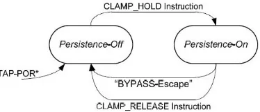
The TMP controller is an FSM, as shown in figure 5, with two states: persistence on and persistence off. State of the controller is determined by decode signals from instruction register and TAP controller output signals. Asynchronous reset options, either TRSTN or POR*, must be provided to reset the controller.
A possible implementation of TMPC is shown in figure 6. TMPC generates reset signals to control the boundary registers and other design specific registers. The TMPC together with the initialisation instruction allows safe switching between mission mode and test mode of system being tested.
TAP Instruction Scan
Instructions maybe loaded in to TAP controller's IR by traversing the TAP state machine down to Update-IR state. At this state, the current contents of the register are shifted out (by TDO) as new value is shifted in. However, the value shifted out will always be fixed with 01 as last to bits, as mandated by the IEEE 1149.1standard for use in testing the functionality of the JTAG interface. The procedure for shifting a bit in and out of either shift register (IR or DR) is identical; the TAP state machine must be in the Shift-IR or Shift-DR state, respectively. The input bit (at TDI) is sampled by the TAP controller on the rising edge of each TCK cycle, while the output bit is driven out on the falling edge of the TCK cycle.
For each bit in the transfer, except the final bit, TMS must remain low. This is important so that, as each bit is shifted in and shifted out, the state machine remains in the Shift-IR
TAP Data Scan
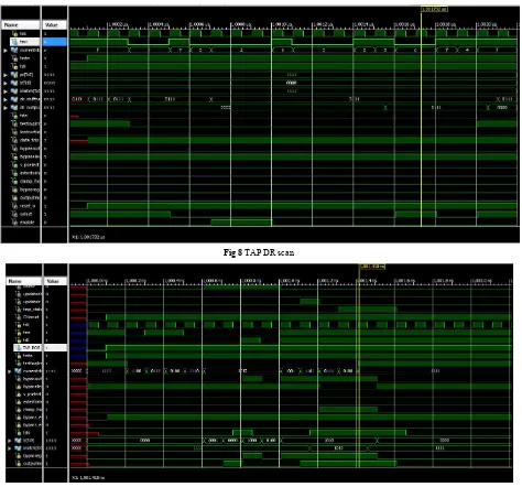
Shifting values into and out of the DR of the TAP controller is performed in a similar manner to that of the IR. The simulation result of data scan is given in figure 8.
Simulation Results of Test Logic
The test logic is simulated using Xilinx ISE design suite and the result is shown in figure 9.
IMPLEMENTATION RESULTS
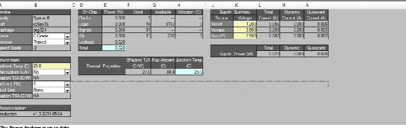
Design is implemented in Xilinx XC6LX16-CS324 evaluation board and results are analyzed. The Xilinx nexys evaluation board is used here for physical design automation (floor planning, placement and rooting). The RTL design is also analyzed using Cadence Encounter™ RTL Compiler. Cadence RTL Compiler is a powerful tool for logic synthesis and analysis for digital designs. The FPGA utilization of TAPC is shown in table 3.
Fig 5 TMP controller state diagram
Fig 6 TMP controller example implementation
Instruction shift operation at IR shift register (ir [3:0]) currentstate [3:0] is at shift_ir state (b)
The area in terms of the cells used is shown in figure 10. -
Alternatively the area may also be represented using number of gate equivalent (GE). The GE is an estimation of hardware design complexity independent from circuit realisation and fabrication technology. One approach to calculate the GE is by dividing design area over area of one GE. Using the values from fig.5 the approximate GE of TAPC is obtained to be 66
Power usage of TAPC in terms of leakage and dynamic power dissipation is shown in figure 12. The leakage power gives the static power dissipation during quiescent condition and dynamic power is the power usage during its normal operation.
Fig 8 TAP DR scan
Fig 9 Test logic simulation waveform
Table 3 Resource utilization of TAP controller
Logic Utilization Used available utilization
Number of slice flip flops 4 1536 1%
Number of 4 input LUTs 13 11536 1%
Number of occupied slices 7 768 1%
Number of bonded IOBs 18 63 28%
IOB latches 7
Number of BUFGMUXs 1 8 12%
Average fan-out of Non-clock nets
7.00
Table 4 Resource utilization of IP core
Logic Utilization Used available utilization
Number of slice flip flops 17 8224 1%
Number of 4 input LUTs 19 9112 1%
Number of occupied slices 10 2278 1%
Number of bonded IOBs 13 232 5%
Number of BUFGMUXs 1 16 6%
International Journal of Current Advanced Research Vol 5, Issue 11, pp 1437-1443, November 2016
Power usage of IP core using XPower analysis tool in terms of leakage and dynamic power dissipation is shown in figure 13. The leakage power gives the static power dissipation during quiescent condition and dynamic power is the power usage during its normal operation.
Tap Controller and Security Issues
Initially JTAG was designed as attest interface without a security concern. Though this scan-chain test approach provides the best controllability to the test engineer, scan chains can be used by an attacker to read chip internal data, stored secret information and determining the position of all the scan elements in a chain. The increased attacks to hardware through jtag port have raised concern over the vulnerability of a device having TAP port. Many defensive techniques have been proposed by both academicians and industrialists for a secure TAP implementation.
Attackers must be denied the use of JTAG port features by applying security mechanisms to prohibit device hacking. It is important, however, that the security mechanism do not interfere with the functionality used by normal users. Security features for JTAG must be cautiously designed and implemented without affecting either security or usability.
[8] present a detailed survey on the state-of-the-art in scan-based side-channel attacks on symmetric and public-key cryptographic hardware implementations. Then the existing scan attack countermeasures are also evaluated for determining their security against known scan attacks and analysed in terms of area, timing and security.
The major issue concerning the security enhancements is the area overhead and operational constraints. Many of security mechanisms using conventional cryptographic algorithms given in [8] will lead to considerable area, power and speed overhead. A series of lightweight block ciphers have been proposed recently which are designed and targeted specifically for extremely constrained environments. LBlock lightweight block cipher, being one among them, can achieve enough security margin against known attacks, such as differential cryptanalysis, linear cryptanalysis, impossible differential cryptanalysis and related-key attacks etc. LBlock can be implemented efficiently not only in hardware environments but also in software platforms such as 8-bit microcontroller. Feistel-type structure suitable for lightweight environment and choice of the rotation constant is made based on the considerations about security and efficient implementation.
LBlock lightweight block cipher algorithm
Lightweight block ciphers are lightweight cryptographic primitives. The main differences between the conventional block ciphers and the lightweight block ciphers are centered on: the block size which is in general 32, 48 or 64 bits for a lightweight block cipher and equal to 64 or 128 bits for a
Fig 11 Gate count of TAP
Fig 12 Power usage of TAPC
conventional block cipher; the same remark also holds for the different possible key sizes (smaller for lightweight block ciphers); Lightweight block ciphers also rely more on elementary operations (such as binary XOR, binary AND, etc.) leading in an increase of required number of rounds. Lightweight block ciphers generally extremely simplify the key schedule due to memory requirements.
LBlock is a light weight block cipher in both hardware and 8-bit platforms and is area efficient. It ciphers blocks of size 64 bits under keys of size 80 bits using 32 rounds of a modified Feistel network. The round function is composed of a subkey addition, 8 S boxes applied in parallel followed by a 4 bits permutation. The LBlock cipher consists of ten s-boxes in parallel. The round function uses eight 4 X 4 S-boxes from s0, s1, S2, s3, s4, s5, s6, s7. The other two s-boxes s8, s9 are used for key scheduling. In the encryption algorithm of LBlock block cipher, the 64 bit plaintext, M is processed by first dividing it into two separate sequences. The encryption procedure involves round function, shifting and xor-ing operations. The components used in each round are: Round function-F which is constructed from two other functions, Confusion function S and Diffusion function P.
The inputs to the LBlock are 64-bit plaintext and 80-bit key. The given plaintext is divided into two equal halves as it uses fiestel structure. One part of the plaintext is directly fed to the round function and the other after performing shifting for xor-ing. The first 32 bits of the 80-bit masterkey is used as the subkey for round-1. This subkey along with one half of plaintext is the input to the round function. The round function-F obtained by doing other two functions called confusion and diffusion. The confusion is created by substitution and diffusion by permutation. The output obtained from the round function and the shifted plaintext are xor-ed to obtain the first intermediate sub ciphertext.
Proposed Security Measures To the Ip Core
The proposed secure test architecture is based on a challenge - response based test protocol using the LBlock [9] light-weight block-cipher. It is a family of flexible hardware-oriented block ciphers, suitable for constrained environments, as in cryptographic applications such as smart cards or RFID chips. To provide unrestricted functions to authentic users while only blocking misuse by attackers, user authentication or test data encryption can be used.
In an unauthenticated state, only user authentication, bypass and device ID (if provided) instructions can be executed while other test instructions are bypassed for security, becoming executable only after a valid authentication. This requires that the authentication logic control the instruction decoder and test registers. The main benefits of the proposed Secure TAP controller are that it uses standard communication and is applicable to standard JTAG environments, and that it does not interfere with normal functions of other TAP connections which do not need security or in an environment where multiple JTAG connections exist in a single device. This is because in the unauthenticated state, Secure JTAG just bypasses all data, allowing the normal data flow. The provision to add user defined instructions in the standard allows to define new instructions for locking and unlocking the device.
Communication of with the IP core is exactly same as defined in the IEEE 1149.1 except for the addition of an authentication operation. The steps involved are:
1. A tester randomly extracts a CRP 2. A challenge is send to the chip.
3. Chip applies the challenge to the LBlock module and sends the result back.
4. User compares the chips response with CRP.
5. If a match is found the regular TAP operation is allowed
This involves use of an additional register to hold the cipher text and a comparator in the authentication module of IP core. The LBlock circuitry may be kept as a separate entity. The hardware implementation of LBlock requires about 1320 GE on 0.18 µm technology with a throughput of 200 Kbps at 100 KHz. In an area-optimized implementation, LBlock requires only 866.3 GE with additional RAM which far less compared to the other conventional ciphers used for TAP defence [8].
CONCLUSIONS
The paper proposes design and implementation of the IEEE 1149.1-2013 TAP controller IP core. The design is synthesised using Xilinx® ISE and implemented in Xilinx nexys 3 evaluation board. The proposed work is fully compatible with the standard and provides a reusable module with a robust and easily testable design. This work is expected to serve as a ready to use module that can be directly inserted in to a new digital IC designs with little modifications. The paper also suggests a security enhancement mechanism for the IP core.
References
1. IEEE Standard 1149.1-2013, ``Standard Test Access Port and Boundary-Scan Architecture''
2. IEEE Standard 1149.1-2001, ``Standard Test Access Port and Boundary-Scan Architecture''.
3. Kenneth P. Parker, “Surviving State Disruptions Caused by Test: the “Lobotomy Problem”,” IEEE International Test Conference 2010.
4. Kenneth P. Parker, David Dubberke, Shuichi Kameyama, “Surviving State Disruptions Caused by Test: A Case Study,” Keysight Technologies, August, 2014.
5. David B. Lavo, “A Good Excuse for Reuse: “Open” TAP Controller Design,” ITC International Test Conference, 2000, p. 1090-1099.
6. Dave Stang, and R. Dandapani, “An implementation of IEEE 1149.1-To avoid violation and other practical In Compliance”, IEEE-2002.
7. Lima, M., F. Santos, J. Bione, T. Lins, and E. Barros, “ ip PROCESS: A Development Process for Soft IP-core with Prototyping in FPGA “, Forum on Design Languages (FDL 2005), Swiss, Sept. 2005.
8. Jean da Rolt et al, “Test Versus Security: Past And Present”, IEEE transactions on emerging topics in computing, vol 2, mqrch 2014
9. Wenling Wu, Lei Zhang “LBlock: A Lightweight Block Cipher” Springer, 2011.