e-ISSN: 2278-067X, p-ISSN: 2278-800X, www.ijerd.com
Volume 9, Issue 3 (December 2013), PP. 34-41
Lossy and Lossless Current-mode Integrators using
CMOS Current Mirrors
Amendra Bhandari
1, Agha A. Husain
2, Manveen S. Chadha
3, Ashish Gupta
41,2 ,3 ,4 Department of Electronics and Communication Engineering I.T.S Engineering College,
Plot No. 46, KP-III, Greater Noida-201306(U.P.)-INDIA.
Abstract:- Analogue design has been historically viewed both in voltage-mode and current-mode dominated
form of signal processing. In literature wide variety of techniques and circuits are available for the design of different current-mode signal processing circuits suitable for VLSI implementation. In this paper we present the major current-mode building blocks using complementary CMOS current-mirror pairs such as current adders and current integrators (lossy and lossless). These building blocks form the basic constitutional blocks for the implementation of second-order continuous-time current-mode active filters. All the proposed circuits presented in this paper were tested in SPICE using 0.5µm CMOS process parameters provided by MOSIS (Agilent) and the results thus obtained were in accordance with the theoretical values.
Keywords:- Complementary CMOS current-mirrors, current-adders, current-mode integrators, active filters,
analog circuit design.
I.
INTRODUCTION
State-of-the-art of analogue integrated circuits design is receiving tremendous boost from the development and application of current-mode processing, which is rapidly dominating traditional voltage-mode designs. Current-mode technique to signal processing has been recently receiving considerable attention, due to the fact that this technique offers one or more of the following advantages: (i) Higher slew rates (ii) Lower power consumption (iii) Higher frequency range of operation (iv) Better accuracy and (v) Improved linearity, over voltage-mode techniques. [1], [2], [8], [11] and [16]. Also, current-mode signal processing is a very attractive approach due to the simplicity in implementing operations such as addition/subtraction, multiplication by a constant, and the potential to operate at higher signal bandwidths than their voltage-mode analogues. Some of the approaches widely investigated so far are current-mode building blocks based current-mode circuits; Gm-C based current-mode circuits, switched capacitor and switched current circuits, Gm-Current-mode translinear and Log-domain circuits. All of them can be employed to devise fully integrable implementation in BiPOLAR, CMOS, and BiCMOS technology.
Although BJTs and FETs are both current output devices often the transistors are assembled into voltage oriented circuits and systems. A key performance feature of current-mode processing is inherent wide bandwidth capability, and in a current amplifier the transistor is useful almost up to its unity-gain bandwidth (fT). Recent advances in IC technologies have meant that state-of-the-art analogue IC design is now able to exploit the potential of current-mode analogue signal processing, providing attractive and elegant solutions for many circuits and system problems.
Interest in current-mode (CM) filters has been growing due to the fact that current-mode devices have wider dynamic range, improved linearity, and extended bandwidth compared with voltage-mode devices [11]. The commonly used circuit techniques for designing current-mode filters are mainly classified into two categories.
(i) One technique is based on the transformation of the voltage-mode circuits to current-mode ones, such
as the adjoint network [12], the RC: CR dual transformation [15] and the inverse-complementary network [19] etc.
(ii) The other technique uses the direct current-mode integrators as the basic cell of the design biquad [2], [6], [9] and higher-order filters [20].
II.
PROPOSED CIRCUITS
mismatch between nMOS and pMOS transistors.
1) Current Adder using Current Mirrors: Figure 1 shows a multi-output current adder based on an nMOS
current mirror where ik (k = 1, 2, …, n) is the input signal current and IB isthe bias current.
I2
0 0
M1
0 +VDD
I2
IB
0
M0
I1
M2
In
Mn
I1
In
Fig. 1: Multi-Output Current Adder
Assuming, that all transistors have an equal aspect ratios (W/L), we have the output current Ik as
B i
k
I
i
I
where,i
i=i
1
i
2
...
i
n.2) Current Integrators using Current Mirrors
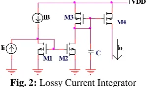
(i) Lossy Current Integrator (Non-Ideal Current Integrator): Figure 2 shows a lossy current integrator which consists of an nMOS and a pMOS current mirror.
+VDD
M3
Ii
M2 M1
M4
C Io IB
Fig. 2: Lossy Current Integrator
The given circuit can easily be extended to a multi-input and multi-output structure by adding input
current sources parallel to ii and output transistors parallel to M4. The output current is given by
I
O
I
B
i
i
where ii is the input signal current and it is assumed that (W/L) ratios are equal. Figure 3 shows the small-signal equivalent circuit of the lossy current integrator shown in Figure 2 where R1 and R3 are the small-signal equivalent resistances of M1 and M3 respectively. From Figure 3, we can obtain the current transfer function TI
(s) as:
3 3 1 4 2
1
sCR
R
R
g
g
i
i
s
T
m mi o I
where, gm2 and gm4 are respectively the transconductance of transistors M2and M4. R1 and R3 are respectively the input resistances of transistors M1 and M3. Thus, we can realize a lossy current integrator which can be also be used as a first-order filter section.
Fig. 3: AC Equivalent Circuit (Lossy Current Integrator)
Io M2
Ii M1
C +VDD
IB
Fig. 4: Simplified Lossy Current Integrator
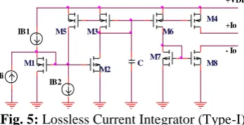
(ii) Lossless Current Integrator (Ideal Current Integrator): Figure 5 shows a lossless current integrator (Type-I). The transistor M5 which provides a positive feedback is added to the lossy current integrator of Figure 2 to cancel the loss of the integrator. IB2 is the DC bias current source of M5, M6, M7, and M8 are also added to obtain an inverted output.
M5
IB1
Ii M2
M7 M1
IB2
M8 M4
- Io
M6
+VDD
M3 +Io
C
Fig. 5: Lossless Current Integrator (Type-I)
Figure 6 shows another lossless integrator structure (Type-II) in which positive feedback is provided through M4 and M5 to cancel the loss of the integrator. This circuit contains fewer transistors than Figure 5. Since lossless integrators have infinite gain at DC, they become unstable when they are used alone due to possible DC offset. Therefore in most applications of the integrators, such as active filters, they are generally used with negative feedback loops. The lossless integrators shown in Figures 5 and 6 contains two DC current sources IB1 and IB2, however IB1 may be provided from the output DC current of a previous stage and IB2 can be canceled by the DC current of a negative feedback loop, thereby simplifying the structure of the circuit.
+VDD
IB2
M6 M4
C
M3 - Io M2
Ii M1
IB1 M5 Io
Fig. 6: Lossless Current Integrator (Type-II)
III.
SIMULATION RESULTS
The workability of the proposed circuits were tested and verified in SPICE using 0.5µm CMOS process parameters provided by MOSIS (AGILENT) as listed in Table-1.
TABLE-1: CMOS PROCESS PARAMETERS
TRANSISTOR PROCESS PARAMETERS
nMOS
LEVEL=3 UO=460.5 TOX=1.0E-8 TPG=1 VTO=0.62 JS=1.08E-6 XJ=0.15U RS=417 RSH=2.73 LD=0.04U VMAX=130E3 NSUB=1.17E17 PB=0.761 ETA=0.00 THETA=0.129 PHI=0.905 GAMMA=0.69 KAPPA=0.10 CJ=76.4E-5 MJ=0.3CJ=76.4E-57 CJSW=CJ=76.4E-5.68E-10 MJSW=0.302 CGSO=1.38E-10 CGDO=1.38E-10 CGBO=3.45E-CGDO=1.38E-10
KF=3.07E-28 AF=1 WD=0.11U DELTA=0.42 NFS=1.2E11
pMOS
LEVEL=3 UO=100 TOX=1.0E-8 TPG=1 VTO=0.58 JS=0.38E-6 XJ=0.10U RS=886 RSH=1.81 LD=0.03U VMAX=113E3 NSUB=2.08E17 PB=0.911 ETA=0.00 THETA=0.120 PHI=0.905 GAMMA=0.76 KAPPA=2 CJ=85E-5 MJ=0.429
value of dc bias current IB = 15µA, C = 1pF, (W/L) ratio = 1µm/1µm and supply voltage VDD = 2.5V. The value of cut-off frequency was found to be fO = 3.5364MHz which was very well in agreement with the calculated theoretical value of fO = 3.5MHz. SPICE simulation results are shown in Figure-7. Figure-8 shows the change in the value of cut-off frequency with change in the value of capacitor. Figure-9 shows the change in the value of gain with change in the value of bias current.
100 102 104 106 108 1010 1012
0 0.1 0.2 0.3 0.4 0.5 0.6 0.7 0.8 0.9 1
Frequency (Hz)
G
ai
n
C=1pF
Fig. 7: First order Low Pass Response of Lossy Current Integrator
100 102 104 106 108 1010 1012
0 0.1 0.2 0.3 0.4 0.5 0.6 0.7 0.8 0.9 1
Frequency (Hz)
G
ai
n
C1=1pF C2=2pF C3=5pF C4=10pF C5=20pF
Fig. 8: Variation in cut-off frequency of Lossy Current Integrator with capacitor
100
102
104
106
108
1010
1012
0 0.1 0.2 0.3 0.4 0.5 0.6 0.7 0.8 0.9 1
Frequeny (Hz)
G
ai
n
IB = 1uA IB=5uA IB=10uA IB=15uA
Fig. 9: Variation in gain of Lossy Current Integrator with bias current
100
101
102
103
104
105
106
107
108
109
1010
0 0.1 0.2 0.3 0.4 0.5 0.6 0.7 0.8 0.9 1
Frequency (Hz)
G
a
in
Fig. 10: First order Low Pass Response of Simplified Lossy Current Integrator
0 0.5 1 1.5 2 2.5 3 3.5 4 4.5 5
x 10-5 -5
-4 -3 -2 -1 0 1x 10
-5
Time (sec)
C
u
rr
e
n
t
(A
) InputOutput
Fig. 11 Response of Simplified Lossy Current Integrator for Square input
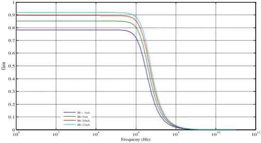
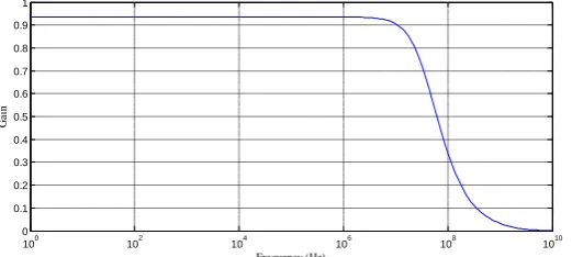
[3] Lossless Current Integrator Type-I (Ideal Current Integrator): For the circuit shown in Figure 5 the ac analysis were carried out with the value of dc bias current IB = 1µA, C = 1pF, (W/L) ratio of pMOS transistor
= 1µm/1µm, (W/L) ratio of nMOS transistor = 1.5µm/10µm and supply voltage VDD = 2.5V. The value of
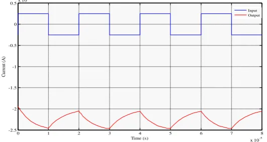
cut-off frequency was found to be fO = 1.9083MHz which was very well in agreement with the calculated theoretical value of fO = 2.0MHz. SPICE simulation results are shown in Figure-12. Figure-13 shows the change in the value of cut-off frequency with change in the value of capacitor. Figure-14 shows the change in the value of gain with change in the value of bias current while Figure 15 shows the integrator response for a square input of amplitude 2.5µA peak value and period of 20µs.
100 102 104 106 108 1010
0 0.1 0.2 0.3 0.4 0.5 0.6 0.7 0.8 0.9 1
Frequency (Hz)
G
a
in
100 102 104 106 108 1010 0
0.1 0.2 0.3 0.4 0.5 0.6 0.7 0.8 0.9
Frequency (Hz)
G
a
in
Fig. 13: First Order Low Pass Response of Lossless Current Integrator (Type-I) for different value of capacitors
100 101 102 103 104 105 106 107 108 109
0 0.1 0.2 0.3 0.4 0.5 0.6 0.7 0.8 0.9 1
Frequency (Hz)
G
a
in
Fig. 14: First Order Low Pass Response of Lossless Current Integrator (Type-I) for various input bias currents
0 1 2 3 4 5 6 7 8
x 10-5 -2.5
-2 -1.5 -1 -0.5 0
0.5x 10
-5
Time (s)
C
ur
re
nt
(
A
)
Input Output
Fig. 15: Response of Lossless Current Integrator (Type-I) for Square input
0 0.5 1 1.5 2 2.5 3 3.5 4 4.5 5
x 10-4 -14
-12 -10 -8 -6 -4 -2 0 2x 10
-6
Time (s)
C
u
r
r
e
n
t
(
A
) InputOutput
Fig. 16: Response of Lossless Current Integrator (Type-II) for Sinusoidal input
0 0.1 0.2 0.3 0.4 0.5 0.6 0.7 0.8 0.9 1
x 10-4 -20
-15 -10 -5 0 5x 10
-6
Time (s)
C
u
rr
e
n
t
(A
)
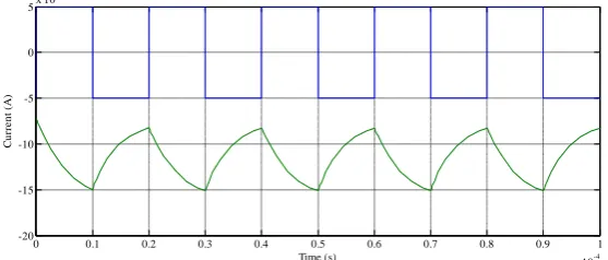
Fig. 17: Response of Lossless Current Integrator (Type-II) for Square input
IV.
CONCLUSIONS
In the given paper current-mode building blocks such as current adders and current integrators (lossy and lossless) have been presented which can be used to form active filters. These active filters are quite suitable for the realization in high frequencies of more than 10MHz. and these filters can operate at a voltage as low as 1.5V or less. The frequency of these filters can be easily and widely controlled by a single DC bias current and this provides good tunability. All the circuits were tested using SPICE and the verified results confirms the theoretical values.
REFERENCES
[1]. J. C. Ahn, and N. Fujii, “Current-mode continuous-time filters using complementary current mirror pairs”, IEICE Trans Fundamentals, vol. E79-A, no.2, pp.168-175, 1996.
[2]. R. Angulo, M. Robinson, and E. S. Sinencio, “Current-mode continuous-time filters: two design approaches”, IEEE Tran. On Circuits and Systems, vol. 39, no. 5, pp. 337-341, 1992.
[3]. R. W. J. Barker, “Accuracy of current mirrors”, IEE Colloquium on Current-mode Analogue Circuits,
London, vol.25, paper 2, 1989.
[4]. B. Gilbert “Wideband negative-current mirror”, Electron Lett., vol.11, pp. 126-127, 1975.
[5]. J. B. Hughes, N. C. Bird, and I. C. Macbeth, “Switched-current: a new technique for analogue
sampled-data signal processing”, IEEE Proc. ISCAS’89, pp. 1584-1587, 1989.
[6]. J. B. Hughes, I. C. Macbeth, and D. M. Pattullo, “Second generation switched-current signal processing”, IEEE Intl. Symposium on Circuits and Systems, 1990.
[7]. D. G. Haig, and J. T. Taylor, “Continuous-time and switched capacitor monolithic filters based on current and charge simulation”, IEEE International Symposium on Circuits and Systems, Portland, USA, vol.3, pp. 1580-1583, 1989.
[8]. S. S. Lee, R. H. Zele, D. J. Allstot, and G. Liang, “A continuous-time current-mode integrator”, IEEE Trans. On Circuits and Systems, vol.39, pp. 1236-1238, 1991.
[9]. S. S. Lee, R. H. Zele, D. J. Allstot, and G. Liang, “CMOS continuous-time current-mode filters for
high frequency applications”, IEEE J. Solid State Circuits, vol.28, no.3, pp. 323-329, 1993.
Peter Peregrinus Ltd., 1990.
[12]. Y. P. Tsividis, “Integrated continuous-time filter design-an overview”, IEEE Journal of Solid-State Circuits, vol.29, issue 3, pp. 166-176, 1994.
[13]. T. Voo, and C. Toumazou, “High-speed current mirror resistive compensation technique”, Electronic Letters, vol.31, no.4, pp. 248-249, 1995.
[14]. T. Voo, and C. Toumazou, C. (1996) “Efficient tunable continuous-time integrated current-mode filter
designs”, IEEE International Symposium on Circuits and Systems, ISCAS '96., Vol. 1, pp. 93 – 96, 1996.
[15]. Z. Wang, and W. Guggenbuhl, “Adjustable bidirectional MOS current mirror/amplifier”, Electron Lett., vol.25, pp. 673-675, 1989.
[16]. B. Wilson, “Current mirrors, amplifiers and dumpers”, Wireless world, vol.87, pp. 47-50, 1981. [17]. B. Wilson, “Design current-output amplifiers using current-mirror circuits”, Electron. Des. News,
vol.27, pp. 121-124, 1982.
[18]. A. M. Ismail, and A. M. Soliman, “Novel CMOS Current Feedback Op-Amp Realization Suitable for
High Frequency Applications”, IEEE Transactions on Circuits and Systems-I: Fundamental Theory and applications,vol. 47, No. 6, pp. 918-921, 2000.
[19]. M. Desai, P. Aronhime, and K. Zurada, “Current-mode network transformation”, IEEE Proc.
ISCAS’94, pp. 599-602, 1994.