Input, Simultaneous Sampling ADC
Data Sheet
AD7606
/
AD7606-6
/
AD7606-4
FEATURES
8/6/4 simultaneously sampled inputs True bipolar analog input ranges: ±10 V, ±5 V Single 5 V analog supply and 2.3 V to 5 V VDRIVE
Fully integrated data acquisition solution Analog input clamp protection
Input buffer with 1 MΩ analog input impedance Second-order antialiasing analog filter
On-chip accurate reference and reference buffer 16-bit ADC with 200 kSPS on all channels Oversampling capability with digital filter Flexible parallel/serial interface
SPI/QSPI™/MICROWIRE™/DSP compatible Performance
7 kV ESD rating on analog input channels 95.5 dB SNR, −107 dB THD ±0.5 LSB INL, ±0.5 LSB DNL Low power: 100 mW Standby mode: 25 mW 64-lead LQFP package
APPLICATIONS
Power-line monitoring and protection systems Multiphase motor control
Instrumentation and control systems Multiaxis positioning systems Data acquisition systems (DAS)
Table 1. High Resolution, Bipolar Input, Simultaneous Sampling DAS Solutions
Resolution Single-Ended Inputs True Differential Inputs Number of Simultaneous Sampling Channels
18 Bits AD7608 AD7609 8
16 Bits AD7606 8
AD7606-6 6
AD7606-4 4
14 Bits AD7607 8
FUNCTIONAL BLOCK DIAGRAM
V1 V1GND RFB 1MΩ 1MΩ RFB CLAMPCLAMP ORDER LPF
SECOND-T/H V2 V2GND RFB 1MΩ 1MΩ RFB CLAMP
CLAMP ORDER LPF
SECOND-T/H V3 V3GND RFB 1MΩ 1MΩ RFB CLAMP
CLAMP ORDER LPF
SECOND-T/H V4 V4GND RFB 1MΩ 1MΩ RFB CLAMP
CLAMP ORDER LPF
SECOND-T/H V5 V5GND RFB 1MΩ 1MΩ RFB CLAMP
CLAMP ORDER LPF
SECOND-T/H V6 V6GND RFB 1MΩ 1MΩ RFB CLAMP
CLAMP ORDER LPF
SECOND-T/H V7 V7GND RFB 1MΩ 1MΩ RFB CLAMP
CLAMP ORDER LPF
SECOND-T/H V8 V8GND RFB 1MΩ 1MΩ RFB CLAMP
CLAMP ORDER LPF
SECOND-T/H 8:1 MUX AGND BUSY FRSTDATA
CONVST A CONVST B RESET RANGE CONTROL INPUTS CLK OSC REFIN/REFOUT REF SELECT AGND OS 2 OS 1 OS 0 DOUTA DOUTB RD/SCLK CS PAR/SER/BYTE SEL VDRIVE 16-BIT SAR DIGITAL FILTER PARALLEL/ SERIAL INTERFACE 2.5V REF REFCAPB REFCAPA SERIAL PARALLEL REGCAP 2.5V LDO REGCAP 2.5V LDO AVCC AVCC DB[15:0] AD7606 08479-001 Figure 1.
TABLE OF CONTENTS
Features ... 1
Applications ... 1
Functional Block Diagram ... 1
Revision History ... 2
General Description ... 3
Specifications ... 4
Timing Specifications ... 7
Absolute Maximum Ratings ... 11
Thermal Resistance ... 11
ESD Caution ... 11
Pin Configurations and Function Descriptions ... 12
Typical Performance Characteristics ... 17
Terminology ... 21
Theory of Operation ... 22
Converter Details... 22
Analog Input ... 22
ADC Transfer Function ... 23
Internal/External Reference ... 24
Typical Connection Diagram ... 25
Power-Down Modes ... 25
Conversion Control ... 26
Digital Interface ... 27
Parallel Interface (PAR/SER/BYTE SEL = 0) ... 27
Parallel Byte (PAR/SER/BYTE SEL = 1, DB15 = 1) ... 27
Serial Interface (PAR/SER/BYTE SEL = 1) ... 27
Reading During Conversion ... 28
Digital Filter ... 29 Layout Guidelines... 32 Outline Dimensions ... 34 Ordering Guide ... 34
REVISION HISTORY
1/12—Rev. B to Rev. C Changes to Analog Input Ranges Section ... 2210/11—Rev. A to Rev. B Changes to Input High Voltage (VINH) and Input Low Voltage (VINL) Parameters and Endnote 6, Table 2 ... 4
Changes to Table 3 ... 7
Changes to Table 4 ... 11
Changes to Pin 32 Description, Table 6 ... 13
Changes to Analog Input Clamp Protection Section ... 22
Changes to Typical Connection Diagram Section ... 25
8/10—Rev. 0 to Rev. A Changes to Note 1, Table 2 ... 6
GENERAL DESCRIPTION
The AD76061/AD7606-6/AD7606-4 are 16-bit, simultaneous
sampling, analog-to-digital data acquisition systems (DAS) with eight, six, and four channels, respectively. Each part contains analog input clamp protection, a second-order antialiasing filter, a track-and-hold amplifier, a 16-bit charge redistribution successive approximation analog-to-digital converter (ADC), a flexible digital filter, a 2.5 V reference and reference buffer, and high speed serial and parallel interfaces.
The AD7606/AD7606-6/AD7606-4 operate from a single 5 V supply and can accommodate ±10 V and ±5 V true bipolar input signals while sampling at throughput rates up to 200 kSPS for all channels. The input clamp protection circuitry can tolerate voltages up to ±16.5 V. The AD7606 has 1 MΩ analog input impedance regardless of sampling frequency. The single supply operation, on-chip filtering, and high input impedance eliminate the need for driver op amps and external bipolar supplies. The AD7606/AD7606-6/AD7606-4 antialiasing filter has a 3 dB cutoff frequency of 22 kHz and provides 40 dB antialias rejection when sampling at 200 kSPS. The flexible digital filter is pin driven, yields improvements in SNR, and reduces the 3 dB bandwidth.
SPECIFICATIONS
VREF = 2.5 V external/internal, AVCC = 4.75 V to 5.25 V, VDRIVE = 2.3 V to 5.25 V, fSAMPLE = 200 kSPS, TA = TMIN to TMAX, unless otherwise noted.1
Table 2.
Parameter Test Conditions/Comments Min Typ Max Unit
DYNAMIC PERFORMANCE fIN = 1 kHz sine wave unless otherwise noted
Signal-to-Noise Ratio (SNR)2, 3 Oversampling by 16; ±10 V range; fIN = 130 Hz 94 95.5 dB
Oversampling by 16; ±5 V range; fIN = 130 Hz 93 94.5 dB
No oversampling; ±10 V Range 88.5 90 dB
No oversampling; ±5 V range 87.5 89 dB
Signal-to-(Noise + Distortion) (SINAD)2 No oversampling; ±10 V range 88 90 dB
No oversampling; ±5 V range 87 89 dB
Dynamic Range No oversampling; ±10 V range 90.5 dB
No oversampling; ±5 V range 90 dB
Total Harmonic Distortion (THD)2 −107 −95 dB
Peak Harmonic or Spurious Noise (SFDR)2 −108 dB
Intermodulation Distortion (IMD)2 fa = 1 kHz, fb = 1.1 kHz
Second-Order Terms −110 dB
Third-Order Terms −106 dB
Channel-to-Channel Isolation2 fIN on unselected channels up to 160 kHz −95 dB
ANALOG INPUT FILTER
Full Power Bandwidth −3 dB, ±10 V range 23 kHz
−3 dB, ±5 V range 15 kHz
−0.1 dB, ±10 V range 10 kHz
−0.1 dB, ±5 V range 5 kHz
tGROUP DELAY ±10 V Range 11 µs
±5 V Range 15 µs
DC ACCURACY
Resolution No missing codes 16 Bits
Differential Nonlinearity2 ±0.5 ±0.99 LSB4
Integral Nonlinearity2 ±0.5 ±2 LSB
Total Unadjusted Error (TUE) ±10 V range ±6 LSB
±5 V range ±12 LSB
Positive Full-Scale Error2, 5 External reference ±8 ±32 LSB
Internal reference ±8 LSB
Positive Full-Scale Error Drift External reference ±2 ppm/°C
Internal reference ±7 ppm/°C
Positive Full-Scale Error Matching2 ±10 V range 5 32 LSB
±5 V range 16 40 LSB
Bipolar Zero Code Error2,6 ±10 V range ±1 ±6 LSB
± 5 V range ±3 ±12 LSB
Bipolar Zero Code Error Drift ±10 V range 10 µV/°C
± 5 V range 5 µV/°C
Bipolar Zero Code Error Matching2 ±10 V range 1 8 LSB
±5 V range 6 22 LSB
Negative Full-Scale Error2, 5 External reference ±8 ±32 LSB
Internal reference ±8 LSB
Negative Full-Scale Error Drift External reference ±4 ppm/°C
Internal reference ±8 ppm/°C
Negative Full-Scale Error Matching2 ±10 V range 5 32 LSB
Parameter Test Conditions/Comments Min Typ Max Unit ANALOG INPUT
Input Voltage Ranges RANGE = 1 ±10 V
RANGE = 0 ±5 V
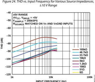
Analog Input Current 10 V; see Figure 31 5.4 µA
5 V; see Figure 31 2.5 µA
Input Capacitance7 5 pF
Input Impedance See the Analog Input section 1 MΩ
REFERENCE INPUT/OUTPUT
Reference Input Voltage Range See the ADC Transfer Function section 2.475 2.5 2.525 V
DC Leakage Current ±1 µA
Input Capacitance7 REF SELECT = 1 7.5 pF
Reference Output Voltage REFIN/REFOUT 2.49/
2.505
V
Reference Temperature Coefficient ±10 ppm/°C
LOGIC INPUTS
Input High Voltage (VINH) 0.7 × VDRIVE V
Input Low Voltage (VINL) 0.3 × VDRIVE V
Input Current (IIN) ±2 µA
Input Capacitance (CIN)7 5 pF
LOGIC OUTPUTS
Output High Voltage (VOH) ISOURCE = 100 µA VDRIVE − 0.2 V
Output Low Voltage (VOL) ISINK = 100 µA 0.2 V
Floating-State Leakage Current ±1 ±20 µA
Floating-State Output Capacitance7 5 pF
Output Coding Twos complement
CONVERSION RATE
Conversion Time All eight channels included; see Table 3 4 µs
Track-and-Hold Acquisition Time 1 µs
Throughput Rate Per channel, all eight channels included 200 kSPS
POWER REQUIREMENTS
AVCC 4.75 5.25 V
VDRIVE 2.3 5.25 V
ITOTAL Digital inputs = 0 V or VDRIVE
Normal Mode (Static) AD7606 16 22 mA
AD7606-6 14 20 mA
AD7606-4 12 17 mA
Normal Mode (Operational)8 f
SAMPLE = 200 kSPS
AD7606 20 27 mA
AD7606-6 18 24 mA
AD7606-4 15 21 mA
Standby Mode 5 8 mA
Parameter Test Conditions/Comments Min Typ Max Unit Power Dissipation
Normal Mode (Static) AD7606 80 115.5 mW
Normal Mode (Operational)8 f
SAMPLE = 200 kSPS AD7606 100 142 mW AD7606-6 90 126 mW AD7606-4 75 111 mW Standby Mode 25 42 mW Shutdown Mode 10 31.5 µW
1 Temperature range for the B version is −40°C to +85°C. The AD7606 is operational up to 125°C with throughput rates ≤ 160 kSPS, and the SNR typically reduces by
0.7 dB at 125°C.
2 See the Terminology section.
3 This specification applies when reading during a conversion or after a conversion. If reading during a conversion in parallel mode with V
DRIVE = 5 V, SNR typically reduces by 1.5 dB
and THD by 3 dB.
4 LSB means least significant bit. With ±5 V input range, 1 LSB = 152.58 µV. With ±10 V input range, 1 LSB = 305.175 µV.
5 These specifications include the full temperature range variation and contribution from the internal reference buffer but do not include the error contribution from
the external reference.
6 Bipolar zero code error is calculated with respect to the analog input voltage. See the Analog Input Clamp Protection section. 7 Sample tested during initial release to ensure compliance.
TIMING SPECIFICATIONS
AVCC = 4.75 V to 5.25 V, VDRIVE = 2.3 V to 5.25 V, VREF = 2.5 V external reference/internal reference, TA = TMIN to TMAX, unless otherwise noted.1
Table 3.
Limit at TMIN, TMAX
(0.1 × VDRIVE and
0.9 × VDRIVE
Logic Input Levels)
Limit at TMIN, TMAX
(0.3 × VDRIVE and
0.7 × VDRIVE
Logic Input Levels)
Parameter Min Typ Max Min Typ Max Unit Description PARALLEL/SERIAL/BYTE MODE
tCYCLE 1/throughput rate
5 5 µs Parallel mode, reading during or after conversion; or serial mode: VDRIVE = 3.3 V to 5.25 V, reading during a
conversion using DOUTA and DOUTB lines
9.4 µs Serial mode reading after a conversion; VDRIVE = 2.7 V
9.7 10.7 µs Serial mode reading after a conversion; VDRIVE = 2.3 V,
DOUTA and DOUTB lines
tCONV2 Conversion time
3.45 4 4.15 3.45 4 4.15 µs Oversampling off; AD7606
3 3 µs Oversampling off; AD7606-6
2 2 µs Oversampling off; AD7606-4
7.87 9.1 7.87 9.1 µs Oversampling by 2; AD7606 16.05 18.8 16.05 18.8 µs Oversampling by 4; AD7606 33 39 33 39 µs Oversampling by 8; AD7606 66 78 66 78 µs Oversampling by 16; AD7606 133 158 133 158 µs Oversampling by 32; AD7606 257 315 257 315 µs Oversampling by 64; AD7606
tWAKE-UP STANDBY 100 100 µs STBY rising edge to CONVST x rising edge; power-up
time from standby mode tWAKE-UP SHUTDOWN
Internal Reference 30 30 ms STBY rising edge to CONVST x rising edge; power-up
time from shutdown mode
External Reference 13 13 ms STBY rising edge to CONVST x rising edge; power-up
time from shutdown mode tRESET 50 50 ns RESET high pulse width
tOS_SETUP 20 20 ns BUSY to OS x pin setup time
tOS_HOLD 20 20 ns BUSY to OS x pin hold time
t1 40 45 ns CONVST x high to BUSY high
t2 25 25 ns Minimum CONVST x low pulse
t3 25 25 ns Minimum CONVST x high pulse
t4 0 0 ns BUSY falling edge to CS falling edge setup time
t53 0.5 0.5 ms Maximum delay allowed between CONVST A, CONVST
B rising edges
t6 25 25 ns Maximum time between last CS rising edge and BUSY
falling edge
t7 25 25 ns Minimum delay between RESET low to CONVST x high
PARALLEL/BYTE READ OPERATION
t8 0 0 ns CS to RD setup time
t9 0 0 ns CS to RD hold time
t10 RD low pulse width
16 19 ns VDRIVE above 4.75 V
21 24 ns VDRIVE above 3.3 V
25 30 ns VDRIVE above 2.7 V
Limit at TMIN, TMAX
(0.1 × VDRIVE and
0.9 × VDRIVE
Logic Input Levels)
Limit at TMIN, TMAX
(0.3 × VDRIVE and
0.7 × VDRIVE
Logic Input Levels)
Parameter Min Typ Max Min Typ Max Unit Description
t13 Delay from CS until DB[15:0] three-state disabled
16 19 ns VDRIVE above 4.75 V
20 24 ns VDRIVE above 3.3 V
25 30 ns VDRIVE above 2.7 V
30 37 ns VDRIVE above 2.3 V
t144 Data access time after RD falling edge
16 19 ns VDRIVE above 4.75 V
21 24 ns VDRIVE above 3.3 V
25 30 ns VDRIVE above 2.7 V
32 37 ns VDRIVE above 2.3 V
t15 6 6 ns Data hold time after RD falling edge
t16 6 6 ns CS to DB[15:0] hold time
t17 22 22 ns Delay from CS rising edge to DB[15:0] three-state
enabled SERIAL READ OPERATION
fSCLK Frequency of serial read clock
23.5 20 MHz VDRIVE above 4.75 V
17 15 MHz VDRIVE above 3.3 V
14.5 12.5 MHz VDRIVE above 2.7 V
11.5 10 MHz VDRIVE above 2.3 V
t18 Delay from CS until DOUTA/DOUTB three-state
disabled/delay from CS until MSB valid 15 18 ns VDRIVE above 4.75 V
20 23 ns VDRIVE above 3.3 V
30 35 ns VDRIVE = 2.3 V to 2.7 V
t194 Data access time after SCLK rising edge
17 20 ns VDRIVE above 4.75 V
23 26 ns VDRIVE above 3.3 V
27 32 ns VDRIVE above 2.7 V
34 39 ns VDRIVE above 2.3 V
t20 0.4 tSCLK 0.4 tSCLK ns SCLK low pulse width
t21 0.4 tSCLK 0.4 tSCLK ns SCLK high pulse width
t22 7 7 SCLK rising edge to DOUTA/DOUTB valid hold time
t23 22 22 ns CS rising edge to DOUTA/DOUTB three-state enabled
FRSTDATA OPERATION
t24 Delay from CS falling edge until FRSTDATA
three-state disabled 15 18 ns VDRIVE above 4.75 V
20 23 ns VDRIVE above 3.3 V
25 30 ns VDRIVE above 2.7 V
30 35 ns VDRIVE above 2.3 V
t25 ns Delay from CS falling edge until FRSTDATA high,
serial mode 15 18 ns VDRIVE above 4.75 V
20 23 ns VDRIVE above 3.3 V
25 30 ns VDRIVE above 2.7 V
30 35 ns VDRIVE above 2.3 V
t26 Delay from RD falling edge to FRSTDATA high
16 19 ns VDRIVE above 4.75 V
20 23 ns VDRIVE above 3.3 V
Limit at TMIN, TMAX
(0.1 × VDRIVE and
0.9 × VDRIVE
Logic Input Levels)
Limit at TMIN, TMAX
(0.3 × VDRIVE and
0.7 × VDRIVE
Logic Input Levels)
Parameter Min Typ Max Min Typ Max Unit Description
t27 Delay from RD falling edge to FRSTDATA low
19 22 ns VDRIVE = 3.3 V to 5.25V
24 29 ns VDRIVE = 2.3 V to 2.7V
t28 Delay from 16th SCLK falling edge to FRSTDATA low
17 20 ns VDRIVE = 3.3 V to 5.25V
22 27 ns VDRIVE = 2.3 V to 2.7V
t29 24 29 ns Delay from CS rising edge until FRSTDATA
three-state enabled
1 Sample tested during initial release to ensure compliance. All input signals are specified with tR = tF = 5 ns (10% to 90% of VDRIVE) and timed from a voltage level of 1.6 V. 2 In oversampling mode, typical t
CONV for the AD7606-6 and AD7606-4 can be calculated using ((N × tCONV) + ((N − 1) × 1 µs)). N is the oversampling ratio. For the AD7606-6,
tCONV = 3 µs; and for the AD7606-4, tCONV = 2 µs.
3 The delay between the CONVST x signals was measured as the maximum time allowed while ensuring a <10 LSB performance matching between channel sets. 4 A buffer is used on the data output pins for these measurements, which is equivalent to a load of 20 pF on the output pins.
Timing Diagrams tCYCLE t3 t5 t2 t4 t1 t7 tRESET tCONV CONVST A, CONVST B CONVST A, CONVST B BUSY CS RESET 08479-002
Figure 2. CONVST Timing—Reading After a Conversion
tCYCLE t3 t5 t6 t2 t1 tCONV CONVST A, CONVST B CONVST A, CONVST B BUSY CS t7 tRESET RESET 08479-003
DATA: DB[15:0] FRSTDATA CS RD INVALID V1 V2 V3 V4 V7 V8 t10 t8 t13 t24 t26 t27 t14 t11 t15 t9 t16 t17 t29 08 47 9-00 4
Figure 4. Parallel Mode, Separate CS and RD Pulses
DATA: DB[15:0] FRSTDATA CS AND RD V1 V2 V3 V4 V5 V6 V7 V8 t12 t13 t16 t 17 0 84 79 -00 5
Figure 5. CS and RD, Linked Parallel Mode
SCLK DOUTA, DOUTB FRSTDATA CS DB15 DB14 DB13 DB1 DB0 t18 t19 t21 t20 t22 t23 t29 t28 t25 084 79 -00 6
Figure 6. Serial Read Operation (Channel 1)
DATA: DB[7:0]
FRSTDATA CS
RD
INVALID BYTE V1HIGH BYTE V1LOW BYTE V8HIGH BYTE V8LOW
t8 t13 t14 t24 t26 t27 t11 t17 t29 t16 t9 t15 t10 08 47 9-00 7
ABSOLUTE MAXIMUM RATINGS
TA = 25°C, unless otherwise noted.Table 4.
Parameter Rating
AVCC to AGND −0.3 V to +7 V
VDRIVE to AGND −0.3 V to AVCC + 0.3 V
Analog Input Voltage to AGND1 ±16.5 V
Digital Input Voltage to AGND −0.3 V to VDRIVE + 0.3 V Digital Output Voltage to AGND −0.3 V to VDRIVE + 0.3 V
REFIN to AGND −0.3 V to AVCC + 0.3 V
Input Current to Any Pin Except Supplies1 ±10 mA Operating Temperature Range
B Version −40°C to +85°C
Storage Temperature Range −65°C to +150°C
Junction Temperature 150°C
Pb/SN Temperature, Soldering
Reflow (10 sec to 30 sec) 240 (+0)°C
Pb-Free Temperature, Soldering Reflow 260 (+0)°C ESD (All Pins Except Analog Inputs) 2 kV
ESD (Analog Input Pins Only) 7 kV
1 Transient currents of up to 100 mA do not cause SCR latch-up.
Stresses above those listed under Absolute Maximum Ratings may cause permanent damage to the device. This is a stress rating only; functional operation of the device at these or any other conditions above those indicated in the operational section of this specification is not implied. Exposure to absolute maximum rating conditions for extended periods may affect device reliability.
THERMAL RESISTANCE
θJA is specified for the worst-case conditions, that is, a device soldered in a circuit board for surface-mount packages. These specifications apply to a 4-layer board.
Table 5. Thermal Resistance
Package Type θJA θJC Unit
64-Lead LQFP 45 11 °C/W
PIN CONFIGURATIONS AND FUNCTION DESCRIPTIONS
AD7606 TOP VIEW (Not to Scale) 64 63 62 61 60 59 58 57 V 1G ND 56 55 54 53 52 51 50 49 V5 V4 V6 V3 V2 V1 PIN 1 V7 V8 V2G ND V 3G ND V 4G ND V 5G ND V 6G ND V 7G ND V 8G ND DB13 DB12 DB11 DB14/ HBE N VDRI V E DB1 17 18 19 20 21 22 23 24 25 AG ND 26 27 28 29 30 31 32 DB2 DB3 DB4 DB5 DB6 DB7/ DO UT A DB9 DB10 DB8/ DO UT B AGND AVCC 1 3 4 FRSTDATA 7 6 5 OS 2 2 8 9 10 12 13 14 15 16 11 DB0 BUSY CONVST B CONVST A RANGE RESET RD/SCLK CS PAR/SER/BYTE SEL OS 1 OS 0 STBYDECOUPLING CAP PIN
DATA OUTPUT POWER SUPPLY ANALOG INPUT GROUND PIN DIGITAL OUTPUT DIGITAL INPUT REFERENCE INPUT/OUTPUT DB15/BYTE SEL REFIN/REFOUT 48 46 45 42 43 44 47 41 40 39 37 36 35 34 33 38 AGND AVCC REFGND REFCAPA AGND AGND AGND REFCAPB REFGND REGCAP REGCAP AVCC AVCC REF SELECT 08479-008
Figure 8. AD7606 Pin Configuration
AD7606-6 TOP VIEW (Not to Scale) 64 63 62 61 60 59 58 57 V 1G ND 56 55 54 53 52 51 50 49 V4 AG ND V5 V3 V2 V1 PIN 1 V6 AG ND V 2G ND V 3G ND AG ND V 4G ND V 5G ND V 6G ND AG ND DB13 DB12 DB11 DB14/ HBE N VDRI V E DB1 17 18 19 20 21 22 23 24 25 AG ND 26 27 28 29 30 31 32 DB2 DB3 DB4 DB5 DB6 DB7/ DO UT A DB9 DB10 DB8/ DO UT B AGND AVCC 1 3 4 FRSTDATA 7 6 5 OS 2 2 8 9 10 12 13 14 15 16 11 DB0 BUSY CONVST B CONVST A RANGE RESET RD/SCLK CS PAR/SER/BYTE SEL OS 1 OS 0 STBY
DECOUPLING CAP PIN
DATA OUTPUT POWER SUPPLY ANALOG INPUT GROUND PIN DIGITAL OUTPUT DIGITAL INPUT REFERENCE INPUT/OUTPUT DB15/BYTE SEL REFIN/REFOUT 48 46 45 42 43 44 47 41 40 39 37 36 35 34 33 38 AGND AVCC REFGND REFCAPA AGND AGND AGND REFCAPB REFGND REGCAP REGCAP AVCC AVCC REF SELECT 08479-009
AD7606-4 TOP VIEW (Not to Scale) 64 63 62 61 60 59 58 57 V 1G ND 56 55 54 53 52 51 50 49 V3 AG ND V4 AG ND V2 V1 PIN 1 AG ND AG ND V 2G ND AG ND AG ND V 3G ND V 4G ND AG ND AG ND DB13 DB12 DB11 DB14/ HBE N VDRI V E DB1 17 18 19 20 21 22 23 24 25 AG ND 26 27 28 29 30 31 32 DB2 DB3 DB4 DB5 DB6 DB7/ DO UT A DB9 DB10 DB8/ DO UT B AGND AVCC 1 3 4 FRSTDATA 7 6 5 OS 2 2 8 9 10 12 13 14 15 16 11 DB0 BUSY CONVST B CONVST A RANGE RESET RD/SCLK CS PAR/SER/BYTE SEL OS 1 OS 0 STBY
DECOUPLING CAP PIN
DATA OUTPUT POWER SUPPLY ANALOG INPUT GROUND PIN DIGITAL OUTPUT DIGITAL INPUT REFERENCE INPUT/OUTPUT DB15/BYTE SEL REFIN/REFOUT 48 46 45 42 43 44 47 41 40 39 37 36 35 34 33 38 AGND AVCC REFGND REFCAPA AGND AGND AGND REFCAPB REFGND REGCAP REGCAP AVCC AVCC REF SELECT 08479-010
Figure 10. AD7606-4 Pin Configuration
Table 6. Pin Function Descriptions
Pin No. Type1
Mnemonic
Description
AD7606 AD7606-6 AD7606-4
1, 37, 38,
48 P AV
CC AVCC AVCC Analog Supply Voltage, 4.75 V to 5.25 V. This supply voltage is applied to the internal front-end amplifiers and to the ADC core. These supply pins should be decoupled to AGND.
2, 26, 35, 40, 41, 47
P AGND AGND AGND Analog Ground. These pins are the ground reference points for all analog
circuitry on the AD7606. All analog input signals and external reference signals should be referred to these pins. All six of these AGND pins should connect to the AGND plane of a system.
5, 4, 3 DI OS [2:0] OS [2:0] OS [2:0] Oversampling Mode Pins. Logic inputs. These inputs are used to select the oversampling ratio. OS 2 is the MSB control bit, and OS 0 is the LSB control bit. See the Digital Filter section for more details about the oversampling mode of operation and Table 9 for oversampling bit decoding.
6 DI PAR/SER/ BYTE SEL PAR/SER/ BYTE SEL PAR/SER/ BYTE SEL
Parallel/Serial/Byte Interface Selection Input. Logic input. If this pin is tied to a logic low, the parallel interface is selected. If this pin is tied to a logic high, the serial interface is selected. Parallel byte interface mode is selected when this pin is logic high and DB15/BYTE SEL is logic high (see Table 8). In serial mode, the RD/SCLK pin functions as the serial clock input. The DB7/DOUTA pin and the DB8/DOUTB pin function as serial data outputs. When the serial interface is selected, the DB[15:9] and DB[6:0] pins should be tied to ground.
In byte mode, DB15, in conjunction with PAR/SER/BYTE SEL, is used to select the parallel byte mode of operation (see Table 8). DB14 is used as the HBEN pin. DB[7:0] transfer the 16-bit conversion results in two RD operations, with DB0 as the LSB of the data transfers.
7 DI STBY STBY STBY Standby Mode Input. This pin is used to place the AD7606/AD7606-6/
AD7606-4 into one of two power-down modes: standby mode or shutdown mode. The power-down mode entered depends on the state of the RANGE pin, as shown in Table 7. When in standby mode, all circuitry, except the on-chip reference, regulators, and regulator buffers, is powered down. When in shutdown mode, all circuitry is powered down.
Pin No. Type1
Mnemonic
Description
AD7606 AD7606-6 AD7606-4
8 DI RANGE RANGE RANGE Analog Input Range Selection. Logic input. The polarity on this pin
deter-mines the input range of the analog input channels. If this pin is tied to a logic high, the analog input range is ±10 V for all channels. If this pin is tied to a logic low, the analog input range is ±5 V for all channels. A logic change on this pin has an immediate effect on the analog input range. Changing this pin during a conversion is not recommended for fast throughput rate applications. See the Analog Input section for more information.
9, 10 DI CONVST A,
CONVST B CONVST A, CONVST B CONVST A, CONVST B Conversion Start Input A, Conversion Start Input B. Logic inputs. These logic inputs are used to initiate conversions on the analog input channels. For simultaneous sampling of all input channels, CONVST A and CONVST B can be shorted together, and a single convert start signal can be applied. Alternatively, CONVST A can be used to initiate simultaneous sampling: V1, V2, V3, and V4 for the AD7606; V1, V2, and V3 for the AD7606-6; and V1 and V2 for the AD7606-4. CONVST B can be used to initiate simultaneous sampling on the other analog inputs: V5, V6, V7, and V8 for the AD7606; V4, V5, and V6 for the AD7606-6; and V3 and V4 for the AD7606-4. This is possible only when oversampling is not switched on. When the CONVST A or CONVST B pin transitions from low to high, the front-end track-and-hold circuitry for the respective analog inputs is set to hold.
11 DI RESET RESET RESET Reset Input. When set to logic high, the rising edge of RESET resets the
AD7606/AD7606-6/AD7606-4. The part should receive a RESET pulse after power-up. The RESET high pulse should typically be 50 ns wide. If a RESET pulse is applied during a conversion, the conversion is aborted. If a RESET pulse is applied during a read, the contents of the output registers reset to all zeros.
12 DI RD/SCLK RD/SCLK RD/SCLK Parallel Data Read Control Input When the Parallel Interface Is Selected (RD)/ Serial Clock Input When the Serial Interface Is Selected (SCLK). When both CS and RD are logic low in parallel mode, the output bus is enabled. In serial mode, this pin acts as the serial clock input for data transfers. The CS falling edge takes the DOUTA and DOUTB data output lines out of three-state and clocks out the MSB of the conversion result. The rising edge of SCLK clocks all subsequent data bits onto the DOUTA and DOUTB serial data outputs. For more information, see the Conversion Control section.
13 DI CS CS CS Chip Select. This active low logic input frames the data transfer. When
both CS and RD are logic low in parallel mode, the DB[15:0] output bus is enabled and the conversion result is output on the parallel data bus lines. In serial mode, CS is used to frame the serial read transfer and clock out the MSB of the serial output data.
14 DO BUSY BUSY BUSY Busy Output. This pin transitions to a logic high after both CONVST A and
CONVST B rising edges and indicates that the conversion process has started. The BUSY output remains high until the conversion process for all channels is complete. The falling edge of BUSY signals that the conversion data is being latched into the output data registers and is available to read after a Time t4. Any data read while BUSY is high must be completed before the falling edge of BUSY occurs. Rising edges on CONVST A or CONVST B have no effect while the BUSY signal is high.
15 DO FRSTDATA FRSTDATA FRSTDATA Digital Output. The FRSTDATA output signal indicates when the first channel, V1, is being read back on the parallel, byte, or serial interface. When the CS input is high, the FRSTDATA output pin is in three-state. The falling edge of CS takes FRSTDATA out of three-state. In parallel mode, the falling edge of RD corresponding to the result of V1 then sets the FRSTDATA pin high, indicating that the result from V1 is available on the output data bus. The FRSTDATA output returns to a logic low following the next falling edge of RD. In serial mode, FRSTDATA goes high on the falling edge of CS because this clocks out the MSB of V1 on DOUTA. It returns low on the 16th SCLK falling edge after the CS falling edge. See the Conversion Control section for more details.
Pin No. Type1
Mnemonic
Description
AD7606 AD7606-6 AD7606-4
22 to 16 DO DB[6:0] DB[6:0] DB[6:0] Parallel Output Data Bits, DB6 to DB0. When PAR/SER/BYTE SEL = 0, these pins act as three-state parallel digital input/output pins. When CS and RD are low, these pins are used to output DB6 to DB0 of the conversion result. When PAR/SER/BYTE SEL = 1, these pins should be tied to AGND. When operating in parallel byte interface mode, DB[7:0] outputs the 16-bit con-version result in two RD operations. DB7 (Pin 24) is the MSB; DB0 is the LSB. 23 P VDRIVE VDRIVE VDRIVE Logic Power Supply Input. The voltage (2.3 V to 5.25 V) supplied at this pin
determines the operating voltage of the interface. This pin is nominally at the same supply as the supply of the host interface (that is, DSP and FPGA). 24 DO DB7/DOUTA DB7/DOUTA DB7/DOUTA Parallel Output Data Bit 7 (DB7)/Serial Interface Data Output Pin (DOUTA).
When PAR/SER/BYTE SEL = 0, this pins acts as a three-state parallel digital input/output pin. When CS and RD are low, this pin is used to output DB7 of the conversion result. When PAR/SER/BYTE SEL = 1, this pin functions as DOUTA and outputs serial conversion data (see the Conversion Control section for more details). When operating in parallel byte mode, DB7 is the MSB of the byte.
25 DO DB8/DOUTB DB8/DOUTB DB8/DOUTB Parallel Output Data Bit 8 (DB8)/Serial Interface Data Output Pin (DOUTB). When PAR/SER/BYTE SEL = 0, this pin acts as a three-state parallel digital input/output pin. When CS and RD are low, this pin is used to output DB8 of the conversion result. When PAR/SER/BYTE SEL = 1, this pin functions as DOUTB and outputs serial conversion data (see the Conversion Control section for more details).
31 to 27 DO DB[13:9] DB[13:9] DB[13:9] Parallel Output Data Bits, DB13 to DB9. When PAR/SER/BYTE SEL = 0, these pins act as three-state parallel digital input/output pins. When CS and RD are low, these pins are used to output DB13 to DB9 of the conversion result. When PAR/SER/BYTE SEL = 1, these pins should be tied to AGND.
32 DO/DI DB14/
HBEN DB14/ HBEN DB14/ HBEN Parallel Output Data Bit 14 (DB14)/High Byte Enable (HBEN). When PAR/ SER/BYTE SEL = 0, this pin acts as a three-state parallel digital output pin. When CS and RD are low, this pin is used to output DB14 of the conversion result. When PAR/SER/BYTE SEL = 1 and DB15/BYTE SEL = 1, the AD7606/ AD7606-6/AD7606-4 operate in parallel byte interface mode. In parallel byte mode, the HBEN pin is used to select whether the most significant byte (MSB) or the least significant byte (LSB) of the conversion result is output first. When HBEN = 1, the MSB is output first, followed by the LSB.
When HBEN = 0, the LSB is output first, followed by the MSB. In serial mode, this pin should be tied to GND.
33 DO/DI DB15/ BYTE SEL DB15/ BYTE SEL DB15/ BYTE SEL
Parallel Output Data Bit 15 (DB15)/Parallel Byte Mode Select (BYTE SEL). When PAR/SER/BYTE SEL = 0, this pin acts as a three-state parallel digital output pin. When CS and RD are low, this pin is used to output DB15 of the conversion result. When PAR/SER/BYTE SEL = 1, the BYTE SEL pin is used to select between serial interface mode and parallel byte interface mode (see Table 8). When PAR/SER/BYTE SEL = 1 and DB15/BYTE SEL = 0, the AD7606 operates in serial interface mode. When PAR/SER/BYTE SEL = 1 and DB15/BYTE SEL = 1, the AD7606 operates in parallel byte interface mode. 34 DI REF SELECT REF SELECT REF SELECT Internal/External Reference Selection Input. Logic input. If this pin is set to logic high, the internal reference is selected and enabled. If this pin is set to logic low, the internal reference is disabled and an external reference voltage must be applied to the REFIN/REFOUT pin.
36, 39 P REGCAP REGCAP REGCAP Decoupling Capacitor Pin for Voltage Output from Internal Regulator.
These output pins should be decoupled separately to AGND using a 1 μF capacitor. The voltage on these pins is in the range of 2.5 V to 2.7 V.
Pin No. Type1
Mnemonic
Description
AD7606 AD7606-6 AD7606-4
42 REF REFIN/
REFOUT REFIN/ REFOUT REFIN/ REFOUT Reference Input (REFIN)/Reference Output (REFOUT). The on-chip reference of 2.5 V is available on this pin for external use if the REF SELECT pin is set to logic high. Alternatively, the internal reference can be disabled by setting the REF SELECT pin to logic low, and an external reference of 2.5 V can be applied to this input (see the Internal/External Reference section). Decoupling is required on this pin for both the internal and external reference options. A 10 μF capacitor should be applied from this pin to ground close to the REFGND pins.
43, 46 REF REFGND REFGND REFGND Reference Ground Pins. These pins should be connected to AGND.
44, 45 REF REFCAPA,
REFCAPB REFCAPA, REFCAPB REFCAPA, REFCAPB Reference Buffer Output Force/Sense Pins. These pins must be connected together and decoupled to AGND using a low ESR, 10 μF ceramic capacitor. The voltage on these pins is typically 4.5 V.
49 AI V1 V1 V1 Analog Input. This pin is a single-ended analog input. The analog input
range of this channel is determined by the RANGE pin.
50, 52 AI GND V1GND,
V2GND V1GND, V2GND V1GND, V2GND Analog Input Ground Pins. These pins correspond to Analog Input Pin V1 and Analog Input Pin V2. All analog input AGND pins should connect to the AGND plane of a system.
51 AI V2 V2 V2 Analog Input. This pin is a single-ended analog input. The analog input
range of this channel is determined by the RANGE pin.
53 AI/GND V3 V3 AGND Analog Input 3. For the AD7606-4, this is an AGND pin.
54 AI GND/
GND
V3GND V3GND AGND Analog Input Ground Pin. For the AD7606-4, this is an AGND pin.
55 AI/GND V4 AGND AGND Analog Input 4. For the AD7606-6 and the AD7606-4, this is an AGND pin.
56 AI GND/
GND
V4GND AGND AGND Analog Input Ground Pin. For the AD7606-6 and AD7606-4, this is an AGND pin.
57 AI V5 V4 V3 Analog Inputs. These pins are single-ended analog inputs. The analog
input range of these channels is determined by the RANGE pin.
58 AI GND V5GND V4GND V3GND Analog Input Ground Pins. All analog input AGND pins should connect to
the AGND plane of a system.
59 AI V6 V5 V4 Analog Inputs. These pins are single-ended analog inputs.
60 AI GND V6GND V5GND V4GND Analog Input Ground Pins. All analog input AGND pins should connect to
the AGND plane of a system.
61 AI/GND V7 V6 AGND Analog Input Pins. For the AD7606-4, this is an AGND pin.
62 AI GND/
GND V7GND V6GND AGND Analog Input Ground Pins. For the AD7606-4, this is an AGND pin.
63 AI/GND V8 AGND AGND Analog Input Pin. For the AD7606-4 and AD7606-6, this is an AGND pin.
64 AI GND/
GND V8GND AGND AGND Analog Input Ground Pin. For the AD7606-4 and AD7606-6, this is an AGND pin.
TYPICAL PERFORMANCE CHARACTERISTICS
0 0 10k 20k 30k 40k 50k 60k 70k 80k 90k 100k –180 –160 –140 –120 –100 –80 –60 –40 –20 AM P L IT UD E ( d B ) INPUT FREQUENCY (Hz) AVCC, VDRIVE = 5V INTERNAL REFERENCE ±10V RANGE FSAMPLE = 200kSPS FIN = 1kHz 16,384 POINT FFT SNR = 90.17dB THD = –106.25dB 08 47 9-0 11Figure 11. AD7606 FFT, ±10 V Range
0 0 10k 20k 30k 40k 50k 60k 70k 80k 90k 100k –180 –160 –140 –120 –100 –80 –60 –40 –20 AM P L IT UD E ( d B ) INPUT FREQUENCY (Hz) AVCC, VDRIVE = 5V INTERNAL REFERENCE ±5V RANGE FSAMPLE = 200kSPS FIN = 1kHz 16,384 POINT FFT SNR = 89.48dB THD = –108.65dB 08 47 9-0 12
Figure 12. AD7606 FFT Plot, ±5 V Range
–180 0 –10 –20 –30 –40 –50 –60 –70 –80 –90 –100 –110 –120 –130 –140 –150 –160 –170 0 0.5 1.0 1.5 2.0 2.5 3.0 3.5 4.0 4.5 5.0 5.5 AM P L IT UD E ( d B ) FREQUENCY (kHz) 0847 9-0 31 AVCC, VDRIVE = 5V INTERNAL REFERENCE ±10V RANGE FSAMPLE = 11.5kSPS TA = 25°C FIN = 133Hz 8192 POINT FFT OS BY 16 SNR = 96.01dB THD = –108.05dB
Figure 13. FFT Plot Oversampling By 16, ±10 V Range
2.0 0 10k 20k 30k 40k 50k 60k –2.0 –1.5 –1.0 –0.5 0 0.5 1.0 1.5 IN L ( L S B ) CODE AVCC, VDRIVE = 5V FSAMPLE = 200kSPS TA = 25°C INTERNAL REFERENCE ±10V RANGE 08 47 9-0 13
Figure 14. AD7606 Typical INL, ±10 V Range
1.0 0 10k 20k 30k 40k 50k 60k –1.0 –0.8 –0.6 –0.4 –0.2 0 0.4 0.2 0.6 0.8 DNL ( L S B) CODE 0847 9-0 14 AVCC, VDRIVE = 5V FSAMPLE = 200kSPS TA = 25°C INTERNAL REFERENCE ±10V RANGE
Figure 15. AD7606 Typical DNL, ±10 V Range
2.0 0 8192 16,384 24,576 32,768 40,960 49,152 57,344 65,536 –2.0 –1.5 –1.0 –0.5 0 0.5 1.0 1.5 IN L ( L S B ) CODE AVCC, VDRIVE = 5V INTERNAL REFERENCE ±5V RANGE FSAMPLE = 200kSPS TA = 25°C 08 47 9-0 15
1.00 0 8192 16,384 24,576 32,768 40,960 49,152 57,344 65,536 –1.00 –0.75 –0.50 –0.25 0 0.25 0.50 0.75 DNL ( L S B) CODE AVCC, VDRIVE = 5V INTERNAL REFERENCE ±5V RANGE FSAMPLE = 200kSPS TA = 25°C 08 47 9-0 16
Figure 17. AD7606 Typical DNL, ±5 V Range
20 15 10 5 0 –5 –10 –15 –40 –25 –10 5 20 35 50 65 80 –20 N F S E RRO R ( L S B ) TEMPERATURE (°C) 0847 9-0 17 200kSPS AVCC, VDRIVE = 5V EXTERNAL REFERENCE ±5V RANGE ±10V RANGE
Figure 18. NFS Error vs. Temperature
20 15 10 5 0 –5 –10 –15 –40 –25 –10 5 20 35 50 65 80 –20 PF S ER R O R ( L S B ) TEMPERATURE (°C) 08 47 9-1 18 200kSPS AVCC, VDRIVE = 5V EXTERNAL REFERENCE ±5V RANGE ±10V RANGE
Figure 19. PFS Error vs. Temperature
10 –40 –25 –10 5 20 35 50 65 80 –10 –9 –6 –4 –2 0 2 4 6 8 NF S /P F S CHANN E L M AT CHI NG ( L S B) TEMPERATURE (°C) 0847 9-0 18 10V RANGE AVCC, VDRIVE = 5V EXTERNAL REFERENCE PFS ERROR NFS ERROR
Figure 20. NFS and PFS Error Matching
10 8 6 4 2 0 0 20k 40k 60k 80k 100k 120k –2 PF S/ N F S ER R O R ( % F S) SOURCE RESISTANCE (Ω) 0847 9-0 19 AVCC, VDRIVE = 5V FSAMPLE = 200 kSPS TA = 25°C EXTERNAL REFERENCE
SOURCE RESISTANCE IS MATCHED ON THE VxGND INPUT
±10V AND ±5V RANGE
Figure 21. PFS and NFS Error vs. Source Resistance
1.0 –40 –25 –10 5 20 35 50 65 80 –1.0 –0.8 –0.6 –0.4 –0.2 0 0.2 0.4 0.6 0.8 BI P O L AR Z E RO CO DE E RRO R ( L S B) TEMPERATURE (°C) 08 47 9-0 23 200kSPS AVCC, VDRIVE = 5V EXTERNAL REFERENCE 5V RANGE 10V RANGE
4 3 2 1 0 –1 –2 –3 –40 –25 –10 5 20 35 50 65 80 –4 BI P O L AR Z E RO CO DE E RRO R M AT CHI NG ( L S B) TEMPERATURE (°C) 08479-024 200kSPS AVCC, VDRIVE = 5V EXTERNAL REFERENCE 5V RANGE 10V RANGE
Figure 23. Bipolar Zero Code Error Matching Between Channels
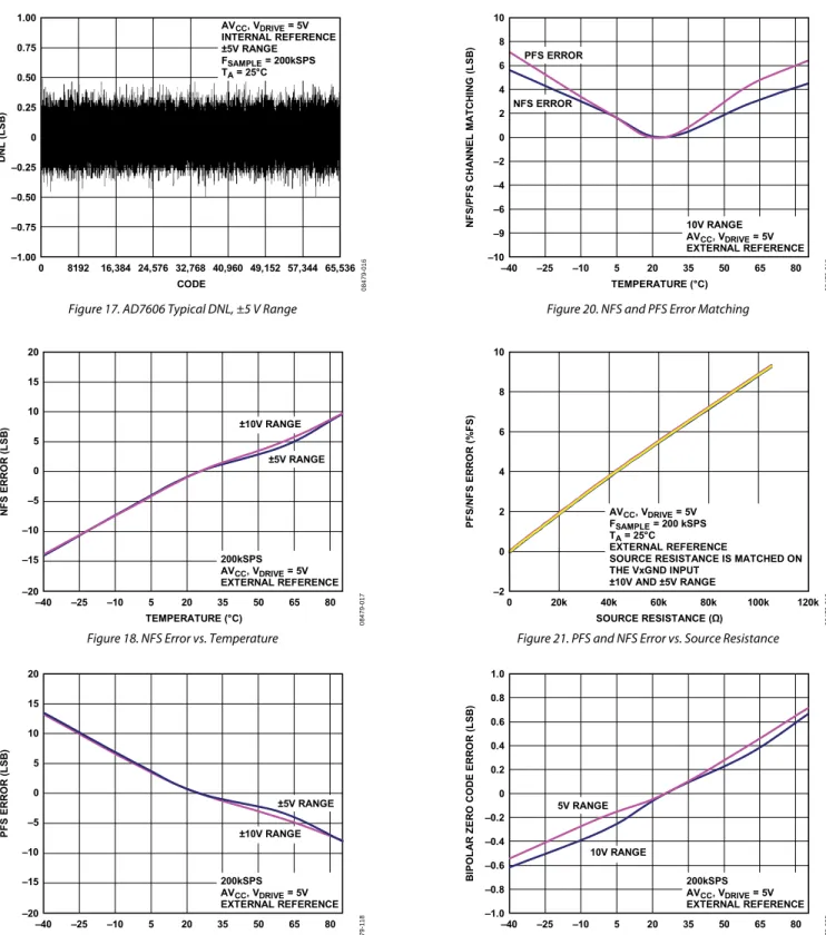
–40 –50 –60 –70 –80 –90 –100 –110 1k 10k 100k –120 T HD ( d B) INPUT FREQUENCY (Hz) 08479-021 ±10V RANGE AVCC, VDRIVE = +5V FSAMPLE = 200kSPS
RSOURCE MATCHED ON Vx AND VxGND INPUTS
105kΩ 48.7kΩ 23.7kΩ 10kΩ 5kΩ 1.2kΩ 100Ω 51Ω 0Ω
Figure 24. THD vs. Input Frequency for Various Source Impedances, ±10 V Range 1k 10k 100k T HD ( d B) INPUT FREQUENCY (Hz) 08479-122 ±5V RANGE AVCC, VDRIVE = +5V FSAMPLE = 200kSPS
RSOURCE MATCHED ON Vx AND VxGND INPUTS
105kΩ 48.7kΩ 23.7kΩ 10kΩ 5kΩ 1.2kΩ 100Ω 51Ω 0Ω –40 –50 –60 –70 –80 –90 –100 –110 –120
Figure 25. THD vs. Input Frequency for Various Source Impedances, ±5 V Range 98 96 94 92 90 88 86 84 82 10 100 1k 10k 100k 80 S NR ( d B) INPUT FREQUENCY (Hz) 08479-020 NO OS OS BY 2 OS BY 4 OS BY 8 OS BY 16 OS BY 32 OS BY 64 AVCC, VDRIVE = 5V
FSAMPLE CHANGES WITH OS RATE
TA = 25°C
INTERNAL REFERENCE ±5V RANGE
Figure 26. SNR vs. Input Frequency for Different Oversampling Rates, ±5 V Range
100 98 96 94 92 90 88 86 84 82 10 100 1k 10k 100k 80 S NR ( d B) INPUT FREQUENCY (Hz) 08479-121 NO OS OS BY 2 OS BY 4 OS BY 8 OS BY 16 OS BY 32 OS BY 64 AVCC, VDRIVE = 5V
FSAMPLE CHANGES WITH OS RATE
TA = 25°C
INTERNAL REFERENCE ±10V RANGE
Figure 27. SNR vs. Input Frequency for Different Oversampling Rates, ±10 V Range
–50 –60 –70 –80 –90 –100 –110 –120 –130 0 20 40 60 80 100 120 140 160 –140 CHANNE L -T O -CHANNE L I S O L AT IO N ( d B) NOISE FREQUENCY (kHz) 08479-025 ±10V RANGE ±5V RANGE AVCC, VDRIVE = 5V INTERNAL REFERENCE
AD7606 RECOMMENDED DECOUPLING USED FSAMPLE = 150kSPS
TA = 25°C
INTERFERER ON ALL UNSELECTED CHANNELS
100 98 96 94 92 90 88 84 86 82 80 DY NAM IC RANG E ( d B) OVERSAMPLING RATIO 08479-026 ±10V RANGE ±5V RANGE AVCC, VDRIVE = 5V TA = 25°C INTERNAL REFERENCE FSAMPLE SCALES WITH OS RATIO
OFF OS2 OS4 OS8 OS16 OS32 OS64
Figure 29. Dynamic Range vs. Oversampling Rate
2.5010 2.5005 2.5000 2.4995 2.4990 2.4985 –40 –25 –10 5 20 35 50 65 80 2.4980 R E FOU T V OLTA GE ( V ) TEMPERATURE (°C) 08479-029 AVCC = 4.75V AVCC = 5V AVCC = 5.25V
Figure 30. Reference Output Voltage vs. Temperature for Different Supply Voltages
8 –10 –8 –6 –4 –2 0 2 4 6 8 10 –10 –8 –6 –4 –2 0 2 4 6 INP UT CURRE NT ( µ A) INPUT VOLTAGE (V) 08479-028 –40°C +25°C +85°C AVCC, VDRIVE = 5V FSAMPLE = 200kSPS
Figure 31. Analog Input Current vs. Temperature for Various Supply Voltages
22 20 18 16 14 12 10 8 AV CC S UP P L Y CURRE NT ( mA) OVERSAMPLING RATIO 08479-027 AVCC, VDRIVE = 5V TA = 25°C INTERNAL REFERENCE FSAMPLE VARIES WITH OS RATE
NO OS OS2 OS4 OS8 OS16 OS32 OS64
Figure 32. Supply Current vs. Oversampling Rate
140 0 100 200 300 400 500 600 700 800 900 10001100 60 70 80 90 100 110 120 130 P O W E R S UP P L Y RE JE CT IO N RAT IO ( d B) AVCC NOISE FREQUENCY (kHz) 08479-030 AVCC, VDRIVE = 5V INTERNAL REFERENCE
AD7606 RECOMMENDED DECOUPLING USED FSAMPLE = 200kSPS
TA = 25°C
±10V RANGE
±5V RANGE
TERMINOLOGY
Integral NonlinearityThe maximum deviation from a straight line passing through the endpoints of the ADC transfer function. The endpoints of the transfer function are zero scale, at ½ LSB below the first code transition; and full scale, at ½ LSB above the last code transition.
Differential Nonlinearity
The difference between the measured and the ideal 1 LSB change between any two adjacent codes in the ADC. Bipolar Zero Code Error
The deviation of the midscale transition (all 1s to all 0s) from the ideal, which is 0 V − ½ LSB.
Bipolar Zero Code Error Match
The absolute difference in bipolar zero code error between any two input channels.
Positive Full-Scale Error
The deviation of the actual last code transition from the ideal last code transition (10 V − 1½ LSB (9.99954) and 5 V − 1½ LSB (4.99977)) after bipolar zero code error is adjusted out. The positive full-scale error includes the contribution from the internal reference buffer.
Positive Full-Scale Error Match
The absolute difference in positive full-scale error between any two input channels.
Negative Full-Scale Error
The deviation of the first code transition from the ideal first code transition (−10 V + ½ LSB (−9.99984) and −5 V + ½ LSB (−4.99992)) after the bipolar zero code error is adjusted out. The negative full-scale error includes the contribution from the internal reference buffer.
Negative Full-Scale Error Match
The absolute difference in negative full-scale error between any two input channels.
Signal-to-(Noise + Distortion) Ratio
The measured ratio of signal-to-(noise + distortion) at the output of the ADC. The signal is the rms amplitude of the fundamental. Noise is the sum of all nonfundamental signals up to half the sampling frequency (fS/2, excluding dc). The ratio depends on the number of quantization levels in the digitization process: the more levels, the smaller the quantization noise.
The theoretical signal-to-(noise + distortion) ratio for an ideal N-bit converter with a sine wave input is given by
Signal-to-(Noise + Distortion) = (6.02 N + 1.76) dB Thus, for a 16-bit converter, the signal-to-(noise + distortion) is 98 dB.
Total Harmonic Distortion (THD)
The ratio of the rms sum of the harmonics to the fundamental. For the AD7606/AD7606-6/AD7606-4, it is defined as
THD (dB) = 20log 1 6 5 4 3 2 V V V V V V V V V 2 9 2 8 2 7 2 2 2 2 2 where:
V1 is the rms amplitude of the fundamental.
V2 to V9 are the rms amplitudes of the second through ninth harmonics.
Peak Harmonic or Spurious Noise
The ratio of the rms value of the next largest component in the ADC output spectrum (up to fS/2, excluding dc) to the rms value of the fundamental. Normally, the value of this specification is determined by the largest harmonic in the spectrum, but for ADCs where the harmonics are buried in the noise floor, it is determined by a noise peak.
Intermodulation Distortion
With inputs consisting of sine waves at two frequencies, fa and fb, any active device with nonlinearities creates distortion products at sum and difference frequencies of mfa ± nfb, where m, n = 0, 1, 2, 3. Intermodulation distortion terms are those for which neither m nor n is equal to 0. For example, the second-order terms include (fa + fb) and (fa − fb), and the third-order terms include (2fa + fb), (2fa − fb), (fa + 2fb), and (fa − 2fb). The calculation of the intermodulation distortion is per the THD specification, where it is the ratio of the rms sum of the individual distortion products to the rms amplitude of the sum of the fundamentals expressed in decibels (dB).
Power Supply Rejection Ratio (PSRR)
Variations in power supply affect the full-scale transition but not the converter’s linearity. PSR is the maximum change in full-scale transition point due to a change in power supply voltage from the nominal value. The PSR ratio (PSRR) is defined as the ratio of the power in the ADC output at full-scale frequency, f, to the power of a 100 mV p-p sine wave applied to the ADC’s VDD and VSS supplies of Frequency fS.
PSRR (dB) = 10 log (Pf/PfS) where:
Pf is equal to the power at Frequency f in the ADC output.
PfS is equal to the power at FrequencyfS coupled onto the AVCC supply.
Channel-to-Channel Isolation
Channel-to-channel isolation is a measure of the level of crosstalk between all input channels. It is measured by applying a full-scale sine wave signal, up to 160 kHz, to all unselected input channels and then determining the degree to which the signal attenuates
THEORY OF OPERATION
CONVERTER DETAILS
The AD7606/AD7606-6/AD7606-4 are data acquisition systems that employ a high speed, low power, charge redistribution, successive approximation analog-to-digital converter (ADC) and allow the simultaneous sampling of eight/six/four analog input channels. The analog inputs on the AD7606/AD7606-6/AD7606-4 can accept true bipolar input signals. The RANGE pin is used to select either ±10 V or ±5 V as the input range. The AD7606/ AD7606-6/AD7606-4 operate from a single 5 V supply. The AD7606/AD7606-6/AD7606-4 contain input clamp protection, input signal scaling amplifiers, a second-order anti-aliasing filter, track-and-hold amplifiers, an on-chip reference, reference buffers, a high speed ADC, a digital filter, and high speed parallel and serial interfaces. Sampling on the AD7606/ AD7606-6/AD7606-4 is controlled using the CONVST signals.
ANALOG INPUT
Analog Input Ranges
The AD7606/AD7606-6/AD7606-4 can handle true bipolar, single-ended input voltages. The logic level on the RANGE pin determines the analog input range of all analog input channels. If this pin is tied to a logic high, the analog input range is ±10 V for all channels. If this pin is tied to a logic low, the analog input range is ±5 V for all channels. A logic change on this pin has an immediate effect on the analog input range; however, there is typically a settling time of approximately 80 µs, in addition to the normal acquisition time requirement. The recommended practice is to hardwire the RANGE pin according to the desired input range for the system signals.
During normal operation, the applied analog input voltage should remain within the analog input range selected via the RANGE pin. A RESET pulse must be applied after power up to ensure the analog input channels are configured for the range selected.
When in a power-down mode, it is recommended to tie the analog inputs to GND. Per the Analog Input Clamp Protection section, the overvoltage clamp protection is recommended for use in transient overvoltage conditions and should not remain active for extended periods. Stressing the analog inputs outside of the conditions mentioned here may degrade the bipolar zero code error and THD performance of the AD7606/AD7606-6/ AD7606-4.
Analog Input Impedance
The analog input impedance of the AD7606/AD7606-6/ AD7606-4 is 1 MΩ. This is a fixed input impedance that does not vary with the AD7606 sampling frequency. This high analog input impedance eliminates the need for a driver amplifier in front of the AD7606/AD7606-6/AD7606-4, allowing for direct connection to the source or sensor. With the need for a driver amplifier eliminated, bipolar supplies (which are often a source of noise in a system) can be removed from the signal chain.
Analog Input Clamp Protection
Figure 34 shows the analog input structure of the AD7606/ AD7606-6/AD7606-4. Each analog input of the AD7606/ AD7606-6/AD7606-4 contains clamp protection circuitry. Despite single 5 V supply operation, this analog input clamp protection allows for an input over voltage of up to ±16.5 V.
1MΩ CLAMP Vx 1MΩ CLAMP VxGND SECOND-ORDER LPF RFB RFB 08479-032
Figure 34. Analog Input Circuitry
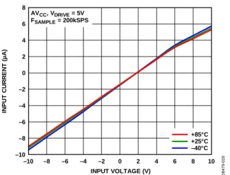
Figure 35 shows the voltage vs. current characteristic of the clamp circuit. For input voltages of up to ±16.5 V, no current flows in the clamp circuit. For input voltages that are above ±16.5 V, the AD7606/AD7606-6/AD7606-4 clamp circuitry turns on.
30 –50 –40 –30 –20 –10 0 10 20 –20 –15 –10 –5 0 5 10 15 20 INP UT CL AM P CURRE NT ( mA) SOURCE VOLTAGE (V) 08479-033 AVCC, VDRIVE = 5V TA = 25°C
Figure 35. Input Protection Clamp Profile
A series resistor should be placed on the analog input channels to limit the current to ±10 mA for input voltages above ±16.5 V. In an application where there is a series resistance on an analog input channel, Vx, a corresponding resistance is required on the analog input GND channel, VxGND (see Figure 36). If there is no corresponding resistor on the VxGND channel, an offset error occurs on that channel. It is recommended that the input overvoltage clamp protection circuitry be used to protect the AD7606/AD7606-6/AD7606-4 against transient overvoltage events. It is not recommended to leave the AD7606/AD7606-6/ AD7606-4 in a condition where the clamp protection circuitry is active in normal or power-down conditions for extended periods because this may degrade the bipolar zero code error performance of the AD7606/AD7606-6/AD7606-4.
1MΩ CLAMP Vx 1MΩ CLAMP VxGND FB RFB C R R ANALOG INPUT SIGNAL AD7606 0 847 9-0 34
Figure 36. Input Resistance Matching on the Analog Input of the AD7606/AD7606-6/AD7606-4
Analog Input Antialiasing Filter
An analog antialiasing filter (a second-order Butterworth) is also provided on the AD7606/AD7606-6/AD7606-4. Figure 37 and Figure 38 show the frequency and phase response, respectively, of the analog antialiasing filter. In the ±5 V range, the −3 dB frequency is typically 15 kHz. In the ±10 V range, the −3 dB frequency is typically 23 kHz. 5 0 –5 –10 –15 –20 –25 –30 –35 –40 100 1k 10k 100k AT T E N UAT IO N ( d B ) INPUT FREQUENCY (Hz) 0847 9-0 35 ±10V RANGE ±5V RANGE AVCC, VDRIVE = 5V FSAMPLE = 200kSPS TA = 25°C ±10V RANGE 0.1dB 3dB –40 10,303 24,365Hz +25 9619 23,389Hz +85 9326 22,607Hz ±5V RANGE 0.1dB 3dB –40 5225 16,162Hz +25 5225 15,478Hz +85 4932 14,990Hz
Figure 37. Analog Antialiasing Filter Frequency Response
18 16 14 12 10 8 6 4 2 0 –2 –4 –6 10 1k 10k 100k –8 P HAS E D E L A Y ( µ s) INPUT FREQUENCY (Hz) 0847 9-0 36 AVCC, VDRIVE = 5V FSAMPLE = 200kSPS TA = 25°C ±5V RANGE ±10V RANGE
Figure 38. Analog Antialias Filter Phase Response
Track-and-Hold Amplifiers
The track-and-hold amplifiers on the AD7606/AD7606-6/ AD7606-4 allow the ADC to accurately acquire an input sine wave of full-scale amplitude to 16-bit resolution. The track-and-hold
hold (that is, the delay time between the external CONVST x signal and the track-and-hold actually going into hold) is well matched, by design, across all eight track-and-holds on one device and from device to device. This matching allows more than one AD7606/AD7606-6/AD7606-4 device to be sampled simultaneously in a system.
The end of the conversion process across all eight channels is indicated by the falling edge of BUSY; and it is at this point that the track-and-holds return to track mode, and the acquisition time for the next set of conversions begins.
The conversion clock for the part is internally generated, and the conversion time for all channels is 4 μs on the AD7606, 3 μs on the AD7606-6, and 2 μs on the AD7606-4. On the AD7606, the BUSY signal returns low after all eight conversions to indicate the end of the conversion process. On the falling edge of BUSY, the track-and-hold amplifiers return to track mode. New data can be read from the output register via the parallel, parallel byte, or serial interface after BUSY goes low; or, alternatively, data from the previous conversion can be read while BUSY is high. Reading data from the AD7606/AD7606-6/AD7606-4 while a conversion is in progress has little effect on performance and allows a faster throughput to be achieved. In parallel mode at VDRIVE > 3.3 V, the SNR is reduced by ~1.5 dB when reading during a conversion.
ADC TRANSFER FUNCTION
The output coding of the AD7606/AD7606-6/AD7606-4 is twos complement. The designed code transitions occur midway between successive integer LSB values, that is, 1/2 LSB and 3/2 LSB. The LSB size is FSR/65,536 for the AD7606. The ideal transfer characteristic for the AD7606/AD7606-6/AD7606-4 is shown in Figure 39. 011...111 011...110 000...001 000...000 111...111 100...010 100...001 100...000 –FS + 1/2LSB 0V – 1/2LSB +FS – 3/2LSB A DC CO DE ANALOG INPUT +FS MIDSCALE –FS LSB ±10V RANGE +10V 0V –10V 305µV ±5V RANGE +5V 0V –5V 152µV +FS – (–FS) 216 LSB = VIN 5V REF 2.5V ±5V CODE = × 32,768 × VIN 10V REF 2.5V ±10V CODE = × 32,768 × 08 47 9-03 7
Figure 39. AD7606/AD7606-6/AD7606-4 Transfer Characteristics The LSB size is dependent on the analog input range selected.
INTERNAL/EXTERNAL REFERENCE
The AD7606/AD7606-6/AD7606-4 contain an on-chip 2.5 V band gap reference. The REFIN/REFOUT pin allows access to the 2.5 V reference that generates the on-chip 4.5 V reference internally, or it allows an external reference of 2.5 V to be applied to the AD7606/AD7606-6/AD7606-4. An externally applied reference of 2.5 V is also gained up to 4.5 V, using the internal buffer. This 4.5 V buffered reference is the reference used by the SAR ADC.
The REF SELECT pin is a logic input pin that allows the user to select between the internal reference and an external reference. If this pin is set to logic high, the internal reference is selected and enabled. If this pin is set to logic low, the internal reference is disabled and an external reference voltage must be applied to the REFIN/REFOUT pin. The internal reference buffer is always enabled. After a reset, the AD7606/AD7606-6/AD7606-4 operate in the reference mode selected by the REF SELECT pin. Decoupling is required on the REFIN/REFOUT pin for both the internal and external reference options. A 10 µF ceramic capacitor is required on the REFIN/REFOUT pin.
The AD7606/AD7606-6/AD7606-4 contain a reference buffer configured to gain the REF voltage up to ~4.5 V, as shown in Figure 40. The REFCAPA and REFCAPB pins must be shorted together externally, and a ceramic capacitor of 10 μF applied to REFGND, to ensure that the reference buffer is in closed-loop operation. The reference voltage available at the REFIN/REFOUT pin is 2.5 V.
When the AD7606/AD7606-6/AD7606-4 are configured in external reference mode, the REFIN/REFOUT pin is a high input impedance pin. For applications using multiple AD7606 devices, the following configurations are recommended, depending on the application requirements.
External Reference Mode
One ADR421 external reference can be used to drive the REFIN/REFOUT pins of all AD7606 devices (see Figure 41). In this configuration, each REFIN/REFOUT pin of the AD7606/AD7606-6/AD7606-4 should be decoupled with at least a 100 nF decoupling capacitor.
Internal Reference Mode
One AD7606/AD7606-6/AD7606-4 device, configured to operate in the internal reference mode, can be used to drive the remaining AD7606/AD7606-6/AD7606-4 devices, which are configured to operate in external reference mode (see Figure 42). The REFIN/ REFOUT pin of the AD7606/AD7606-6/AD7606-4, configured in internal reference mode, should be decoupled using a 10 µF ceramic decoupling capacitor. The other AD7606/AD7606-6/ AD7606-4 devices, configured in external reference mode, should use at least a 100 nF decoupling capacitor on their REFIN/REFOUT pins. BUF SAR 2.5V REF REFCAPA REFIN/REFOUT REFCAPB 10µF 08479-038
Figure 40. Reference Circuitry
AD7606 REF SELECT REFIN/REFOUT AD7606 REF SELECT REFIN/REFOUT 100nF 0.1µF 100nF AD7606 REF SELECT REFIN/REFOUT 100nF ADR421 08479-040
Figure 41. Single External Reference Driving Multiple AD7606/AD7606-6/ AD7606-4 REFIN Pins
AD7606 REF SELECT REFIN/REFOUT + 10µF AD7606 REF SELECT REFIN/REFOUT 100nF AD7606 REF SELECT REFIN/REFOUT 100nF VDRIVE 08479-039
Figure 42. Internal Reference Driving Multiple AD7606/AD7606-6/AD7606-4 REFIN Pins