R01AN2782EJ0100 Rev. 1.00 Page 1 of 41 Apr. 16, 2015
RL78/G14
Pulse Output Forced Cutoff Using the Clock Alarm Function and ELC CC-RL
Abstract
This document describes how to forcibly cut off the pulse output using a combination of the RL78/G14 real-time clock (alarm interrupt function) and the event link controller (ELC).
Products
RL78/G14
When using this application note with other Renesas MCUs, careful evaluation is recommended after making modifications to comply with the alternate MCU.
R01AN2782EJ0100 Rev. 1.00 Apr. 16, 2015
R01AN2782EJ0100 Rev. 1.00 Page 2 of 41 Apr. 16, 2015
Contents
1. Specifications ... 3
2. Operation Confirmation Conditions ... 3
3. Hardware ... 4
3.1 Hardware Configuration ... 4
3.2 Pin Used ... 4
4. Software ... 5
4.1 Operation Overview ... 5
4.2 Option Byte Settings ... 6
4.3 Functions ... 7
4.4 Function Specifications ... 7
4.5 Flowcharts ... 10
4.5.1 Overall Flowchart ... 10
4.5.2 Initialization ... 10
4.5.3 Peripheral Function Initialization ... 11
4.5.4 CPU Clock Initialization ... 12
4.5.5 RTC Initialization ... 13
4.5.6 RTC Start Setting ... 22
4.5.7 RTC Alarm Enable ... 23
4.5.8 ELC Initialization ... 26
4.5.9 Timer RD0 Initialization ... 27
4.5.10 Timer RD0 Start Setting ... 37
4.5.11 Main Processing ... 40
4.5.12 Main Initialization ... 40
5. Sample Code ... 41
R01AN2782EJ0100 Rev. 1.00 Page 3 of 41 Apr. 16, 2015
1. Specifications
In this application note, the PWM signal output from the TRDIOB0 pin is stopped using the pulse output forced cutoff function when an alarm interrupt of the real-time clock (RTC) is generated.
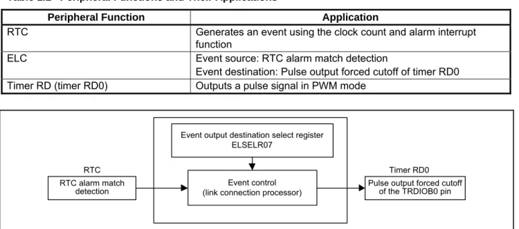
Table 1.1 lists the peripheral functions and their applications. Figure 1.1 shows the relationship among peripheral functions.
Table 1.1 Peripheral Functions and Their Applications
Peripheral Function Application
RTC Generates an event using the clock count and alarm interrupt
function
ELC Event source: RTC alarm match detection
Event destination: Pulse output forced cutoff of timer RD0 Timer RD (timer RD0) Outputs a pulse signal in PWM mode
Event output destination select register ELSELR07
Event control (link connection processor) RTC alarm match
detection Pulse output forced cutoff of the TRDIOB0 pin
RTC Timer RD0
Figure 1.1 Relationship Among Peripheral Functions
2. Operation
Confirmation
Conditions
The sample code accompanying this application note has been run and confirmed under the conditions below.
Table 2.1 Operation Confirmation Conditions
Item Contents
MCU used RL78/G14 (R5F104PJA)
Operating frequencies High-speed on-chip oscillator clock (fHOCO): 32 MHz (typ.)
CPU/peripheral hardware clock (fCLK): 32 MHz
RTC operating clock (fSUB): 32.768 kHz (typ.) Operating voltage 5.0 V (operation enabled from 2.9 to 5.5 V)
LVD operation (VLVD): 2.81 V at the rising edge or 2.75 V at the falling edge in reset mode
Integrated development environment (CS+)
Renesas Electronics Corporation CS+ V3.01.00
C compiler (CS+) Renesas Electronics Corporation CC-RL V1.01.00
Integrated development environment (e2 studio)
Renesas Electronics Corporation e2 studio V4.0.0.26
C compiler (e2 studio) Renesas Electronics Corporation
R01AN2782EJ0100 Rev. 1.00 Page 4 of 41 Apr. 16, 2015
3. Hardware
3.1 Hardware
Configuration
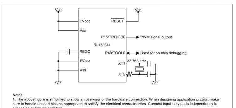
Figure 3.1 shows a connection example.
Figure 3.1 Connection Example
3.2 Pin
Used
Table 3.1 lists the pin used and its function.
Table 3.1 Pin Used and Its Function
Pin Name I/O Function
R01AN2782EJ0100 Rev. 1.00 Page 5 of 41 Apr. 16, 2015
4. Software
4.1 Operation
Overview
After the RTC is started, an alarm interrupt is generated at the time specified by the alarm function. The ELC outputs a request of the pulse output forced cutoff to timer RD0 using the alarm interrupt as an event. Then, the PWM signal output from the TRDIOB0 pin is stopped.
Settings for the peripheral functions are listed below: RTC
Select the subsystem clock (fSUB) as the RTC operating clock
For 12-/24-hour mode setting, specify 24-hour mode
Set the initial value as 0:00:00, Tuesday, January 1, 2013
Set the alarm for 2:00 a.m. every day
Enable an alarm interrupt (an alarm interrupt is used as a source to activate the ELC)
Disable the fixed-cycle interrupt
ELC
Set the alarm match detection as the event source
Set the pulse output forced cutoff of timer RD0 as the event destination
Timer RD0
Specify the PWM function as the operating mode
Select the fCLK (32 MHz) as the count source
Specify the PWM period as 100 μs
Specify the duty cycle as 50%
Use the TRDIOB0 pin, and set the initial output level as not active, and the output signal level as active high
Enable the forced cutoff by an event input signal from the ELC
R01AN2782EJ0100 Rev. 1.00 Page 6 of 41 Apr. 16, 2015
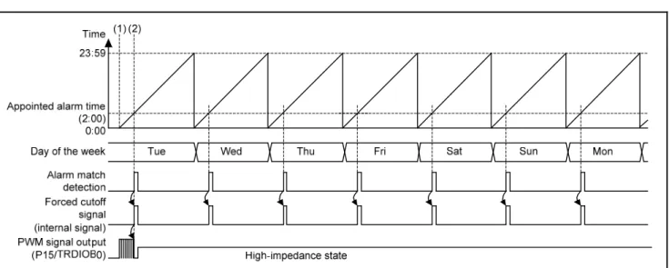
Figure 4.1 Timing Diagram
(1) RTC and timer RD0 start, alarm function enabled
Start the RTC and timer RD0, and enable the alarm function. (2) Alarm match
When the RTC time matches the appointed day of the week and time, an alarm match interrupt is generated. The ELC outputs a forced cutoff signal to timer RD0 when it detects the alarm match.
PWM signaloutput from timer RD0 is stopped by the pulse forced cutoff function.
4.2
Option Byte Settings
Table 4.1 lists the option byte settings.
Table 4.1 Option Byte Settings
Address Setting Value Contents
000C0H/010C0H 11101111B Stops the watchdog timer
(counting is stopped when a reset is canceled)
000C1H/010C1H 01111111B Sets the LVD in reset mode
Detection voltage: 2.81 V at the rising edge, 2.75 V at the falling edge
000C2H/010C2H 11101000B Sets the HOCO clock as 32 MHz in high-speed main (HS) mode
R01AN2782EJ0100 Rev. 1.00 Page 7 of 41 Apr. 16, 2015
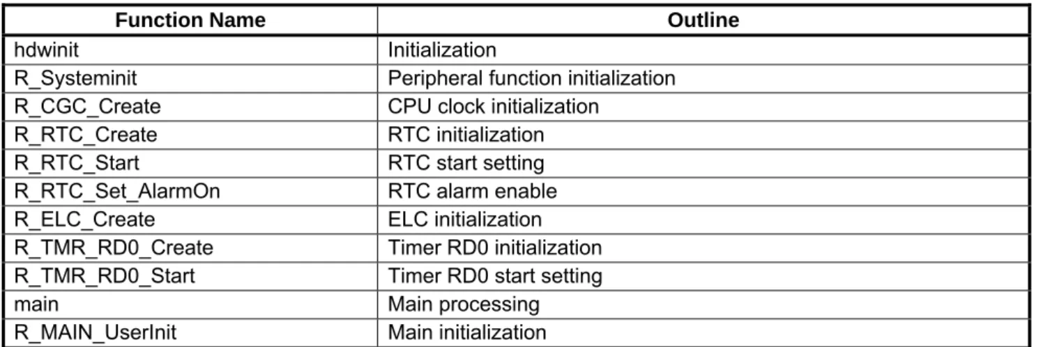
4.3 Functions
Table 4.2 lists the functions.
Table 4.2 Functions
Function Name Outline
hdwinit Initialization
R_Systeminit Peripheral function initialization
R_CGC_Create CPU clock initialization
R_RTC_Create RTC initialization
R_RTC_Start RTC start setting
R_RTC_Set_AlarmOn RTC alarm enable
R_ELC_Create ELC initialization
R_TMR_RD0_Create Timer RD0 initialization
R_TMR_RD0_Start Timer RD0 start setting
main Main processing
R_MAIN_UserInit Main initialization
4.4 Function
Specifications
The following tables list the sample code function specifications.
hdwinit
Outline Initialization
Header None
Declaration void hdwinit(void)
Description Initializes the peripheral functions.
Arguments None
Return Value None
R_Systeminit
Outline Peripheral function initialization
Header None
Declaration void R_Systeminit(void)
Description Initializes the peripheral function used in this application note.
Arguments None
R01AN2782EJ0100 Rev. 1.00 Page 8 of 41 Apr. 16, 2015
R_CGC_Create
Outline CPU clock initialization Header r_cg_cgc.h
Declaration void R_CGC_Create(void) Description Initializes the CPU clock.
Arguments None
Return Value None
R_RTC_Create
Outline RTC initialization Header r_cg_rtc.h
Declaration void R_RTC_Create(void) Description Initializes the RTC.
Arguments None
Return Value None
R_RTC_Start
Outline RTC start setting Header r_cg_rtc.h
Declaration void R_RTC_Start(void)
Description Sets the RTC to operation-enabled status.
Arguments None
Return Value None
R_RTC_Set_AlarmOn
Outline RTC alarm enable Header r_cg_rtc.h
Declaration void R_RTC_Set_AlarmOn(void)
Description Enables the alarm function in operation-enabled status.
Arguments None
Return Value None
R_RTC_Create
Outline ELC initialization Header r_cg_elc.h
Declaration void R_ELC_Create(void) Description Initializes the ELC.
Arguments None
R01AN2782EJ0100 Rev. 1.00 Page 9 of 41 Apr. 16, 2015
R_TMR_RD0_Create
Outline Timer RD0 initialization Header r_cg_timer.h
Declaration void R_TMR_RD0_Create(void)
Description Initializes timer RD0 for use in the PWM function.
Arguments None
Return Value None
R_TMR_RD0_Start
Outline Timer RD0 start setting Header r_cg_timer.h
Declaration void R_TMR_RD0_Start(void)
Description Sets timer RD0 to operation-enabled status.
Arguments None
Return Value None
main
Outline Main processing
Header None
Declaration void main(void)
Description Performs the main processing.
Arguments None
Return Value None
R_MAIN_UserInit
Outline Main initialization
Header None
Declaration void R_MAIN_UserInit(void)
Description Performs processing required to initialize the main processing.
Arguments None
R01AN2782EJ0100 Rev. 1.00 Page 10 of 41 Apr. 16, 2015
4.5 Flowcharts
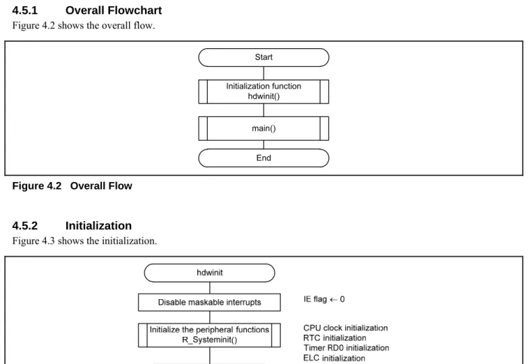
4.5.1 Overall Flowchart
Figure 4.2 shows the overall flow.
Start
End Initialization function
hdwinit()
main()
Figure 4.2 Overall Flow
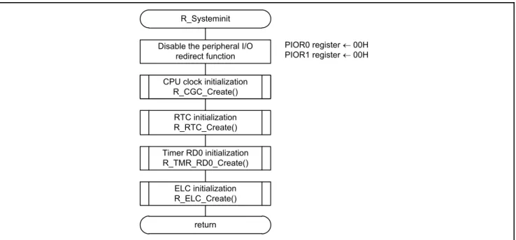
4.5.2 Initialization
Figure 4.3 shows the initialization.
R01AN2782EJ0100 Rev. 1.00 Page 11 of 41 Apr. 16, 2015
4.5.3 Peripheral Function Initialization
Figure 4.4 shows the peripheral function initialization.
R_Systeminit Disable the peripheral I/O
redirect function
PIOR0 register 00H
PIOR1 register 00H
return Initialize the CPU R_CGC_Create() CPU clock initialization
R_CGC_Create() RTC initialization R_RTC_Create() Timer RD0 initialization R_TMR_RD0_Create() ELC initialization R_ELC_Create()
R01AN2782EJ0100 Rev. 1.00 Page 12 of 41 Apr. 16, 2015
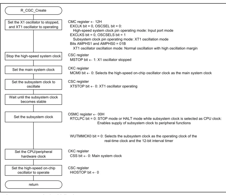
4.5.4 CPU Clock Initialization
Figure 4.5 shows the CPU clock initialization.
R_CGC_Create Set the X1 oscillator to stopped,
and XT1 oscillator to operating
return
Stop the high-speed system clock CSC register
MSTOP bit 1: X1 oscillator stopped
Set the main system clock CKC register
MCM0 bit 0: Selects the high-speed on-chip oscillator clock as the main system clock Set the subsystem clock to
oscillate
CSC register
XTSTOP bit 0: XT1 oscillator operating
CKC register
CSS bit 0: Main system clock
Set the CPU/peripheral hardware clock Set the high-speed on-chip
oscillator to operate
CSC register
HIOSTOP bit 0
Set the subsystem clock OSMC registerRTCLPC bit = 0: STOP mode or HALT mode while subsystem clock is selected as CPU clock:00H Enables supply of subsystem clock to peripheral functions
WUTMMCK0 bit = 0: Selects the subsystem clock as the operating clock of the real-time clock and the 12-bit interval timer
CMC register 12H
EXCLK bit = 0, OSCSEL bit = 0:
High-speed system clock pin operating mode: Input port mode EXCLKS bit = 0, OSCSELS bit = 1
Subsystem clock pin operating mode: XT1 oscillation mode Bits AMPHS1 and AMPHS0 = 01B
XT1 oscillator oscillation mode: Normal oscillation with high oscillation margin
Wait until the subsystem clock becomes stable
R01AN2782EJ0100 Rev. 1.00 Page 13 of 41 Apr. 16, 2015
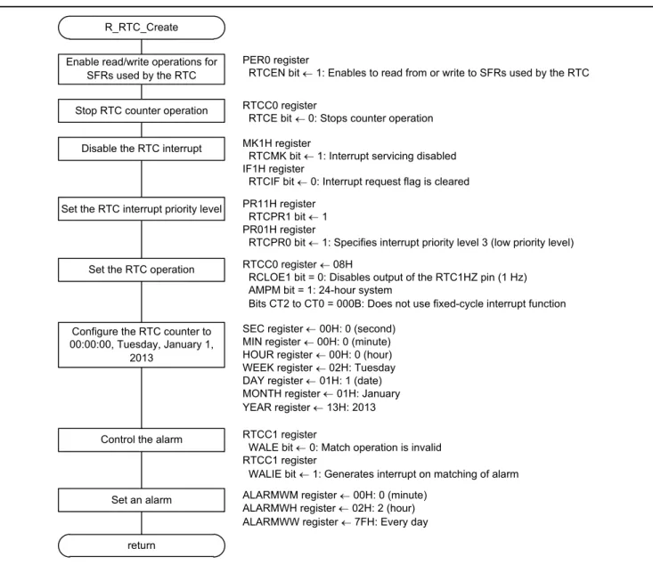
4.5.5 RTC Initialization
Figure 4.6 shows the RTC initialization.
R_RTC_Create
Stop RTC counter operation RTCC0 register
RTCE bit 0: Stops counter operation
Disable the RTC interrupt MK1H register
RTCMK bit 1: Interrupt servicing disabled IF1H register
RTCIF bit 0: Interrupt request flag is cleared
Control the alarm RTCC1 register
WALE bit 0: Match operation is invalid RTCC1 register
WALIE bit 1: Generates interrupt on matching of alarm
return
Enable read/write operations for SFRs used by the RTC
PER0 register
RTCEN bit 1: Enables to read from or write to SFRs used by the RTC
Set the RTC interrupt priority level PR11H register
RTCPR1 bit 1
PR01H register
RTCPR0 bit 1: Specifies interrupt priority level 3 (low priority level)
Set the RTC operation RTCC0 register 08H
RCLOE1 bit = 0: Disables output of the RTC1HZ pin (1 Hz) AMPM bit = 1: 24-hour system
Bits CT2 to CT0 = 000B: Does not use fixed-cycle interrupt function Configure the RTC counter to
00:00:00, Tuesday, January 1, 2013
SEC register 00H: 0 (second)
MIN register 00H: 0 (minute)
HOUR register 00H: 0 (hour)
WEEK register 02H: Tuesday
DAY register 01H: 1 (date)
MONTH register 01H: January
YEAR register 13H: 2013
Set an alarm ALARMWM register 00H: 0 (minute)
ALARMWH register 02H: 2 (hour)
ALARMWW register 7FH: Every day
R01AN2782EJ0100 Rev. 1.00 Page 14 of 41 Apr. 16, 2015
Enabling read and write operations for SFRs used by the RTC
Peripheral enable register 0 (PER0)
Symbol 7 6 5 4 3 2 1 0
PER0 RTCEN IICA1EN ADCEN IICA0EN SAU1EN SAU0EN TAU1EN TAU0EN
Value 1 × × × × × × ×
Bit 7
RTCEN
bit Control of real-time clock (RTC) and 12-bit interval timer input clock supply
0
Stops input clock supply
SFRs used by the real-time clock (RTC) and 12-bit interval timer cannot be written
1
Enables input clock supply
SFRs used by the real-time clock (RTC) and 12-bit interval timer can be read and written
Stopping RTC counter operation
Real-time clock control register 0 (RTCC0)
Symbol 7 6 5 4 3 2 1 0
RTCC0 RTCE 0 RCLOE1 0 AMPM CT2 CT1 CT0
Value 0 ‒ ‒
Bit 7
RTCE bit Real-time clock operation control
0 Stops counter operation
1 Starts counter operation
For details on register setting, refer to the RL78/G14 User’s Manual: Hardware.
Legend symbol:
R01AN2782EJ0100 Rev. 1.00 Page 15 of 41 Apr. 16, 2015
Disabling the RTC interrupt
Interrupt mask flag register (MK1H)
Symbol 7 6 5 4 3 2 1 0 MK1H TMMK10 TRJMK0 SRMK3 CSIMK31 IICMK31 STMK3 CSIMK30 IICMK30 KRMK ITMK RTCMK ADMK Value × × × × × × 1 × Bit 1 RTCMK
bit Interrupt servicing control
0 Interrupt servicing enabled
1 Interrupt servicing disabled
Interrupt request flag register (IF1H)
Symbol 7 6 5 4 3 2 1 0
IF1H TMIF10 TRJIF0 SRIF3 CSIIF31
IICIF31
STIF3 CSIIF30
IICIF30
KRIF ITIF RTCIF ADIF
Value × × × × × × 0 ×
Bit 1
RTCIF bit Interrupt request flag
0 No interrupt request signal is generated
1 Interrupt request signal is generated, interrupt request status For details on register setting, refer to the RL78/G14 User’s Manual: Hardware.
Legend symbol:
R01AN2782EJ0100 Rev. 1.00 Page 16 of 41 Apr. 16, 2015
Setting the RTC interrupt priority level
Priority specification flag registers (PR11H, PR01H)
Symbol 7 6 5 4 3 2 1 0 PR11H TMPR110 TRJPR10 SRPR13 CSIPR131 IICPR131 STPR13 CSIPR130 IICPR130 KRPR1 ITPR1 RTCPR1 ADPR1 Value × × × × × × 1 × Symbol 7 6 5 4 3 2 1 0 PR01H TMPR010 TRJPR00 SRPR03 CSIPR031 IICPR031 STPR03 CSIPR030 IICPR030 KRPR0 ITPR0 RTCPR0 ADPR0 Value × × × × × × 1 × Bit 1 RTCPR1 bit RTCPR0
bit Priority level selection
0 0 Specifies level 0 (high priority level) 0 1 Specifies level 1
1 0 Specifies level 2
1 1 Specifies level 3 (low priority level)
For details on register setting, refer to the RL78/G14 User’s Manual: Hardware.
Legend symbol:
R01AN2782EJ0100 Rev. 1.00 Page 17 of 41 Apr. 16, 2015
Setting the RTC operation
Real-time clock control register 0 (RTCC0)
Output signals from the RTC1HZ pin: Disabled
12-hour or 24-hour mode: 24-hour mode
Fixed-cycle interrupt function: Not used
Symbol 7 6 5 4 3 2 1 0
RTCC0 RTCE 0 RCLOE1 0 AMPM CT2 CT1 CT0
Value ‒ 0 ‒ 1 0 0 0
Bit 5
RCLOE1
bit RTC1HZ pin output control
0 Disables output of the RTC1HZ pin (1 Hz)
1 Enables output of the RTC1HZ pin (1 Hz) Bit 3
AMPM
bit Selection of 12-/24-hour system
0 12-hour system (a.m. and p.m. are displayed)
1 24-hour system
Bits 2 to 0
CT2 bit CT1 bit CT0 bit Fixed-cycle interrupt (INTRTC) selection 0 0 0 Does not use fixed-cycle interrupt function
0 0 1 Once every 0.5 seconds (synchronized with counting up seconds) 0 1 0 Once per second (same time as counting up seconds) 0 1 1 Once per minute (second 00 every minute)
1 0 0 Once per hour (minute 00 and second 00 every hour) 1 0 1 Once per day (hour 00, minute 00, and second 00 every day) 1 1 × Once per month (date 1, hour 00 a.m., minute 00, and second 00 every month)
For details on register setting, refer to the RL78/G14 User’s Manual: Hardware.
Legend symbol:
R01AN2782EJ0100 Rev. 1.00 Page 18 of 41 Apr. 16, 2015
Configuring the RTC counter
Second count register (SEC) Sets the second to 0.
Symbol 7 6 5 4 3 2 1 0
SEC 0 SEC40 SEC20 SEC10 SEC8 SEC4 SEC2 SEC1
Value ‒ 0 0 0 0 0 0 0
Function Bits 6 to 0 Specify a decimal value of 00 to 59 in BCD code
Minute count register (MIN) Sets the minute to 0.
Symbol 7 6 5 4 3 2 1 0
MIN 0 MIN40 MIN20 MIN10 MIN8 MIN4 MIN2 MIN1
Value ‒ 0 0 0 0 0 0 0
Function Bits 6 to 0 Specify a decimal value of 00 to 59 in BCD code
Hour count register (HOUR) Sets the hour to 0.
Symbol 7 6 5 4 3 2 1 0
HOUR 0 0 HOUR20 HOUR10 HOUR8 HOUR4 HOUR2 HOUR1
Value ‒ ‒ 0 0 0 0 0 0
Function Bits 5 to 0 Specify a decimal value of 00 to 23, or 01 to 12 or 21 to 32 in BCD code
Day count register (DAY) Sets the date to 1.
Symbol 7 6 5 4 3 2 1 0
DAY 0 0 DAY20 DAY10 DAY8 DAY4 DAY2 DAY1
Value ‒ ‒ 0 0 0 0 0 1
Function Bits 5 to 0 Specify a decimal value of 01 to 31 in BCD code
For details on register setting, refer to the RL78/G14 User’s Manual: Hardware.
Legend symbol:
R01AN2782EJ0100 Rev. 1.00 Page 19 of 41 Apr. 16, 2015
Week count register (WEEK) Sets the day of the week to Tuesday.
Symbol 7 6 5 4 3 2 1 0
WEEK 0 0 0 0 0 WEEK4 WEEK2 WEEK1
Value ‒ ‒ ‒ ‒ ‒ 0 1 0
Function Bits 2 to 0 Specify a decimal value of 00 to 06 in BCD code
Month count register (MONTH) Sets the month to January.
Symbol 7 6 5 4 3 2 1 0
MONTH 0 0 0 MONTH10 MONTH8 MONTH4 MONTH2 MONTH1
Value ‒ ‒ ‒ 0 0 0 0 1
Function Bits 4 to 0 Specify a decimal value of 01 to 12 in BCD code
Year count register (YEAR) Sets the year to 2013.
Symbol 7 6 5 4 3 2 1 0
YEAR YEAR80 YEAR40 YEAR20 YEAR10 YEAR8 YEAR4 YEAR2 YEAR1
Value 0 0 0 1 0 0 1 1
Function Bits 7 to 0 Specify a decimal value of 00 to 99 in BCD code
For details on register setting, refer to the RL78/G14 User’s Manual: Hardware.
Legend symbol:
R01AN2782EJ0100 Rev. 1.00 Page 20 of 41 Apr. 16, 2015
Controlling the alarm
Real-time clock control register 1 (RTCC1)
Alarm match operation: Invalid
An interrupt when an alarm matches: Generated
Symbol 7 6 5 4 3 2 1 0
RTCC1 WALE WALIE 0 WAFG RIFG 0 RWST RWAIT
Value 0 1 ‒ ‒
Bit 7
WALE bit Alarm operation control
0 Match operation is invalid
1 Match operation is valid Bit 6
WALIE
bit Alarm detection status flag
0 Does not generate interrupt on matching of alarm
1 Generates interrupt on matching of alarm Setting an alarm
Alarm minute register (ALARMWM) Sets the minute value to 0.
Symbol 7 6 5 4 3 2 1 0
ALARMWM 0 WM40 WM20 WM10 WM8 WM4 WM2 WM1
Value ‒ 0 0 0 0 0 0 0
Function Bits 6 to 0 Specify a decimal value of 00 to 59 in BCD code
Alarm hour register (ALARMWH) Sets the hour value to 2.
Symbol 7 6 5 4 3 2 1 0
ALARMWH 0 0 WH20 WH10 WH8 WH4 WH2 WH1
Value ‒ ‒ 0 0 0 0 1 0
Function Bits 5 to 0 Specify a decimal value of 00 to 23, or 01 to 12 or 21 to 32 in BCD code
For details on register setting, refer to the RL78/G14 User’s Manual: Hardware.
Legend symbol:
R01AN2782EJ0100 Rev. 1.00 Page 21 of 41 Apr. 16, 2015
Alarm week register (ALARMWW) Sets the day of the week value to every day.
Symbol 7 6 5 4 3 2 1 0
ALARMWW 0 WW6 WW5 WW4 WM3 WW2 WW1 WW0
Value ‒ 1 1 1 1 1 1 1
Bits 6 to 0
Day of the week
alarm sounds Function
WW6 Saturday 0 Disables an alarm
1 Enables an alarm
WW5 Friday 0 Disables an alarm
1 Enables an alarm
WW4 Thursday 0 Disables an alarm
1 Enables an alarm
WW3 Wednesday 0 Disables an alarm
1 Enables an alarm
WW2 Tuesday 0 Disables an alarm
1 Enables an alarm
WW1 Monday 0 Disables an alarm
1 Enables an alarm
WW0 Sunday 0 Disables an alarm
1 Enables an alarm
For details on register setting, refer to the RL78/G14 User’s Manual: Hardware.
Legend symbol:
R01AN2782EJ0100 Rev. 1.00 Page 22 of 41 Apr. 16, 2015
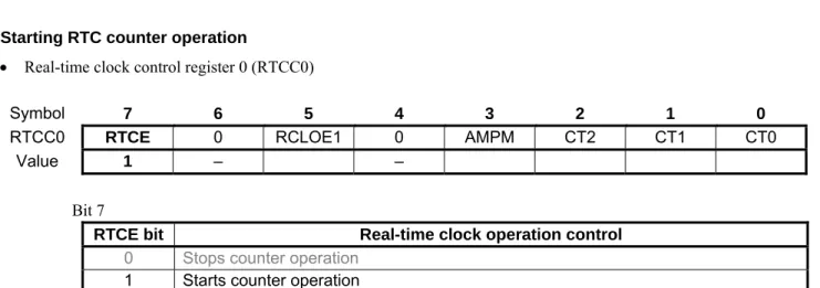
4.5.6 RTC Start Setting
Figure 4.7 shows the setting to start RTC counter operation.
Figure 4.7 RTC Start Setting
Starting RTC counter operation
Real-time clock control register 0 (RTCC0)
Symbol 7 6 5 4 3 2 1 0
RTCC0 RTCE 0 RCLOE1 0 AMPM CT2 CT1 CT0
Value 1 ‒ ‒
Bit 7
RTCE bit Real-time clock operation control
0 Stops counter operation
1 Starts counter operation
For details on register setting, refer to the RL78/G14 User’s Manual: Hardware.
Legend symbol:
R01AN2782EJ0100 Rev. 1.00 Page 23 of 41 Apr. 16, 2015
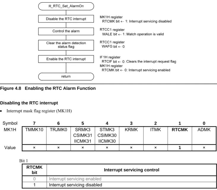
4.5.7 RTC Alarm Enable
Figure 4.8 shows the setting to enable the RTC alarm function.
Figure 4.8 Enabling the RTC Alarm Function
Disabling the RTC interrupt
Interrupt mask flag register (MK1H)
Symbol 7 6 5 4 3 2 1 0 MK1H TMMK10 TRJMK0 SRMK3 CSIMK31 IICMK31 STMK3 CSIMK30 IICMK30 KRMK ITMK RTCMK ADMK Value × × × × × × 1 × Bit 1 RTCMK
bit Interrupt servicing control
0 Interrupt servicing enabled
1 Interrupt servicing disabled
For details on register setting, refer to the RL78/G14 User’s Manual: Hardware.
Legend symbol:
R01AN2782EJ0100 Rev. 1.00 Page 24 of 41 Apr. 16, 2015
Controlling the alarm
Real-time clock control register 1 (RTCC1)
Symbol 7 6 5 4 3 2 1 0
RTCC1 WALE WALIE 0 WAFG RIFG 0 RWST RWAIT
Value 1 ‒ × ‒ × ×
Bit 7
WALE bit Alarm operation control
0 Match operation is invalid
1 Match operation is valid Clearing the alarm detection status flag
Real-time clock control register (RTCC1)
Symbol 7 6 5 4 3 2 1 0
RTCC1 WALE WALIE 0 WAFG RIFG 0 RWST RWAIT
Value ‒ 0 × ‒ × ×
Bit 4
WAFG bit Alarm detection status flag
0 Alarm mismatch
1 Detection of matching of alarm
For details on register setting, refer to the RL78/G14 User’s Manual: Hardware.
Legend symbol:
R01AN2782EJ0100 Rev. 1.00 Page 25 of 41 Apr. 16, 2015
Enabling the RTC interrupt
Interrupt request flag register (IF1H)
Symbol 7 6 5 4 3 2 1 0
IF1H TMIF10 TRJIF0 SRIF3 CSIIF31
IICIF31
STIF3 CSIIF30
IICIF30
KRIF ITIF RTCIF ADIF
Value × × × × × × 0 ×
Bit 1
RTCIF bit Interrupt request flag
0 No interrupt request signal is generated
1 Interrupt request signal is generated, interrupt request status
Interrupt mask flag register (MK1H)
Symbol 7 6 5 4 3 2 1 0 MK1H TMMK10 TRJMK0 SRMK3 CSIMK31 IICMK31 STMK3 CSIMK30 IICMK30 KRMK ITMK RTCMK ADMK Value × × × × × × 0 × Bit 1 RTCMK
bit Interrupt servicing control
0 Interrupt servicing enabled
1 Interrupt servicing disabled
For details on register setting, refer to the RL78/G14 User’s Manual: Hardware.
Legend symbol:
R01AN2782EJ0100 Rev. 1.00 Page 26 of 41 Apr. 16, 2015
4.5.8 ELC Initialization
Figure 4.9 shows the ELC initialization.
Figure 4.9 ELC Initialization
Setting the event destination
Event output destination select register 07 (ELSELR07)
Register Name Event Generator (Output Origin of Event Input 7) Event Description
ELSELR07 RTC fixed-cycle signal/alarm match detection INTRTC
Symbol 7 6 5 4 3 2 1 0
ELSELR07 0 0 0 0 ELSEL3 ELSEL2 ELSEL1 ELSEL0
Value ‒ ‒ ‒ ‒ 0 1 1 0 Bits 3 to 0 ELSEL3 bit ELSEL2 bit ELSEL1 bit ELSEL0
bit Event link selection
0 0 0 0 Event link disabled
0 0 0 1 Selects operation of peripheral function to link 0 0 1 0 Selects operation of peripheral function to link 0 0 1 1 Selects operation of peripheral function to link 0 1 0 0 Selects operation of peripheral function to link 0 1 0 1 Selects operation of peripheral function to link
0 1 1 0
Link destination peripheral function: Timer RD0 Operation when an event is acknowledged: TRDIOD0 input capture, pulse output forced cutoff
0 1 1 1 Selects operation of peripheral function to link 1 0 0 0 Selects operation of peripheral function to link 1 0 0 1 Selects operation of peripheral function to link For details on register setting, refer to the RL78/G14 User’s Manual: Hardware.
Legend symbol:
R01AN2782EJ0100 Rev. 1.00 Page 27 of 41 Apr. 16, 2015
4.5.9 Timer RD0 Initialization
Figure 4.10 and Figure 4.11 show the timer RD0 initialization.
R_TMR_RD0_Create
Specify timer RD0 count operation
TRDSTR register
CSEL0 bit 1: Continues counting after compare match
with TRDGRA0 register Enable read and write operations
for SFRs used by timer RD PER1 registerTRD0EN bit 1: Enables to read from or write to SFRs used by timer RD
Set timer RD0 to stop counting TRDSTR register
TSTART0 bit 0: Count stops
Disable the timer RD0 interrupt MK2H register
TRDMK0 bit 1: Interrupt servicing disabled IF2H register
TRDIF0 bit 0: Clears the interrupt request flag Enable ELC event input 0
for timer RD pulse output forced cutoff
TRDELC register
ELCOBE0 bit 1: Forced cutoff is enabled
Set registers TRDGRD0 and TRDGRC0 as general registers
TRDMR register
TRDBFD0 bit 0: TRDGRD0 register function: general register
TRDBFC0 bit 0: TRDGRC0 register function: general register
Specify the PWM function for timer RD
TRDPMR register
TRDPWMB0 bit 1: TRDIOB0 PWM function: PWM function
Set the pulse output forced cutoff TRDDF0 register 10H
Bits PENB1 and PENB0 = 01B: TRDIOB0 pin pulse output forced cutoff: high-impedance output
Bits DFD and DFC = 00B: TRDIOC0 pin pulse output forced cutoff: disabled Bits DFB and DFA = 00B: TRDIOD0 pin pulse output forced cutoff: disabled
Set an output from timer RD0 TRDOER1 register
ED0 bit 1: Output from the TRDIOD0 pin disabled
EC0 bit 1: Output from the TRDIOC0 pin disabled
EB0 bit 0: Output from the TRDIOB0 pin enabled
EA0 bit 1: Output from the TRDIOA0 pin disabled
Set the initial output level from the TRDIOB0 pin
TRDOCR register
TOB0 bit 0: Specifies the initial output level as not active
Control timer RD0 TRDCR0 register
Bits CCLR2 to CCLR0 001B: Clears the TRD0 counter by compare match with
TRDGRA0 register
Bits TCK2 to TCK0 000B: Specifies the count source for timer RD0 as fCLK, and fHOCO
A
R01AN2782EJ0100 Rev. 1.00 Page 28 of 41 Apr. 16, 2015
Figure 4.11 Timer RD0 Initialization (2/2)
Enabling read and write operations for SFRs used by timer RD
Peripheral enable register 1 (PER1)
Symbol 7 6 5 4 3 2 1 0
PER1 DACEN TRGEN CMPEN TRD0EN DTCEN 0 0 TRJ0EN
Value × × × 1 × ‒ ‒ ×
Bit 4
TRD0EN
bit Control of timer RD input clock supply
0
Stops input clock supply
SFR used by timer RD cannot be written.
Timer RD is in the reset status.
1 Enables input clock supply
SFR used by timer RD can be read and written.
For details on register setting, refer to the RL78/G14 User’s Manual: Hardware.
Legend symbol:
R01AN2782EJ0100 Rev. 1.00 Page 29 of 41 Apr. 16, 2015
Specifying timer RD0 count operation
Timer RD start register (TRDSTR)
Symbol 7 6 5 4 3 2 1 0
TRDSTR 0 0 0 0 CSEL1 CSEL0 TSTART1 TSTART0
Value ‒ ‒ ‒ ‒ × 1 ×
Bit 2
CSEL0
bit TRD0 count operation select
0 Count stops at a compare match with TRDGRA0 register
1 Count continues after compare match with TRDGRA0 register
Setting timer RD0 to stop counting
Timer RD start register (TRDSTR)
Symbol 7 6 5 4 3 2 1 0
TRDSTR 0 0 0 0 CSEL1 CSEL0 TSTART1 TSTART0
Value ‒ ‒ ‒ ‒ × × 0
Bit 0
TSTART0
bit TRD0 count start flag
0 Count stops
1 Count starts
For details on register setting, refer to the RL78/G14 User’s Manual: Hardware.
Legend symbol:
R01AN2782EJ0100 Rev. 1.00 Page 30 of 41 Apr. 16, 2015
Disabling the RD0 interrupt
Interrupt mask flag register (MK2H)
Symbol 7 6 5 4 3 2 1 0 MK2H FLMK IICAMK1 1 SREMK3 TMMK13H TRGMK TRDMK1 TRDMK0 PMK11 CMPMK1 Value × × ‒ × × × 1 × Bit 1 TRDMK0
bit Interrupt servicing control
0 Interrupt servicing enabled
1 Interrupt servicing disabled
Interrupt request flag register (IF2H)
Symbol 7 6 5 4 3 2 1 0
IF2H FLIF IICAIF1 0 SREIF3
TMIF13H
TRGIF TRDIF1 TRDIF0 PIF11
CMPIF1
Value × × ‒ × × × 0 ×
Bit 1
TRDIF0
bit Interrupt request flag
0 No interrupt request signal is generated
1 Interrupt request signal is generated, interrupt request status
Enabling ELC event input 0 for timer RD pulse output forced cutoff
Timer RD ELC register (TRDELC)
Symbol 7 6 5 4 3 2 1 0
TRDELC 0 0 ELCOBE1 ELCICE1 0 0 ELCOBE0 ELCICE0
Value ‒ ‒ × × ‒ ‒ 1 ×
Bit 1
ELCOBE0
bit ELC event input 0 enable for timer RD pulse output forced cutoff
0 Forced cutoff is disabled
1 Forced cutoff is enabled
For details on register setting, refer to the RL78/G14 User’s Manual: Hardware.
Legend symbol:
R01AN2782EJ0100 Rev. 1.00 Page 31 of 41 Apr. 16, 2015
Setting registers TRDGRD0 and TRDGRC0 as general registers
Timer RD mode register (TRDMR)
Symbol 7 6 5 4 3 2 1 0
TRDMR TRDBFD1 TRDBFC1 TRDBFD0 TRDBFC0 0 0 0 TRDSYNC
Value × × 0 0 ‒ ‒ ‒
Bit 5
TRDBFD0
bit TRDGRD0 register function select
0 General register
1 Buffer register for TRDGRB0 register Bit 4
TRDBFC0
bit TRDGRC0 register function select
0 General register
1 Buffer register for TRDGRA0 register
Specifying the PWM function for timer RD
Timer RD PWM function select register (TRDPMR)
Symbol 7 6 5 4 3 2 1 0
TRDPMR 0 TRDPWMD1 TRDPWMC1 TRDPWMB1 0 TRDPWMD0 TRDPWMC0 TRDPWMB0
Value ‒ × × × ‒ × × 1
Bit 0
TRDPWMB0
bit PWM function of TRDIOB0 select
0 Input capture function or output compare function
1 PWM function
For details on register setting, refer to the RL78/G14 User’s Manual: Hardware.
Legend symbol:
R01AN2782EJ0100 Rev. 1.00 Page 32 of 41 Apr. 16, 2015
Setting the pulse output forced cutoff
Timer RD digital filter function select register 0 (TRDDF0)
TRDIOB0 pin pulse output forced cutoff: High-impedance output
TRDIOC0 pin pulse output forced cutoff: Disabled
TRDIOD0 pin pulse output forced cutoff: Disabled
Symbol 7 6 5 4 3 2 1 0
TRDDF0 DFCK1 DFCK0 PENB1 PENB0 DFD DFC DFB DFA
Value 0 1 0 0 0 0
Bits 5 and 4
PENB1 bit
PENB0
bit TRDIOB0 pin pulse forced cutoff control
0 0 Forced cutoff disabled
0 1 High-impedance output
1 0 Low output
1 1 High output
Bits 3 and 2
DFD bit DFC bit TRDIOC0 pin digital filter function select
0 0 Forced cutoff disabled
0 1 High-impedance output
1 0 Low output
1 1 High output
Bits 1 and 0
DFB bit DFA bit TRDIOD0 pin digital filter function select
0 0 Forced cutoff disabled
0 1 High-impedance output
1 0 Low output
1 1 High output
For details on register setting, refer to the RL78/G14 User’s Manual: Hardware.
Legend symbol:
R01AN2782EJ0100 Rev. 1.00 Page 33 of 41 Apr. 16, 2015
Setting an output from timer RD0
Timer RD output master enable register 1 (TRDOER1)
Symbol 7 6 5 4 3 2 1 0
TRDOER1 ED1 EC1 EB1 EA1 ED0 EC0 EB0 EA0
Value × × × × 1 1 0 1
Bit 3
ED0 bit TRDIOD0 output disable
0 Output enabled
1 Output disabled (TRDIOD0 pin functions as an I/O port)
Bit 2
EC0 bit TRDIOC0 output disable
0 Output enabled
1 Output disabled (TRDIOC0 pin functions as an I/O port)
Bit 1
EB0 bit TRDIOB0 output disable
0 Output enabled
1 Output disabled (TRDIOB0 pin is functions as an I/O port)
Bit 0
EA0 bit TRDIOA0 output disable
0 Output enabled
1 Output disabled (TRDIOA0 pin functions as an I/O port) Setting the initial output level from the TRDIOB0 pin
Timer RD output control register (TRDOCR)
Symbol 7 6 5 4 3 2 1 0
TRDOCR TOD1 TOC1 TOB1 TOA1 TOD0 TOC0 TOB0 TOA0
Value × × × × × × 0 ×
Bit 1
TOB0 bit TRDIOB0 initial output level select
0 Low initial output
1 High initial output
For details on register setting, refer to the RL78/G14 User’s Manual: Hardware.
Legend symbol:
R01AN2782EJ0100 Rev. 1.00 Page 34 of 41 Apr. 16, 2015
Controlling timer RD0
Timer RD control register 0 (TRDCR0)
TRD0 counter is cleared by: A compare match with the TRDGRA0 register
Count source: fCLK Symbol 7 6 5 4 3 2 1 0 TRDCR0 CCLR2 CCLR1 CCLR0 CKEG1 CKEG0 TCK2 TCK1 TCK0 Value 0 0 1 × × 0 0 0 Bits 7 to 5 CCLR2 bit CCLR1 bit CCLR0
bit TRD0 counter clear select
0 0 0 Clear disabled (free-running operation)
0 0 1 Clear by input capture or compare match with TRDGRA0
0 1 0 Clear by input capture or compare match with TRDGRB0 0 1 1 Synchronous clear (clear simultaneously with other timer RD0 counter) 1 0 0 Do not set.
1 0 1 Clear by input capture or compare match with TRDGRC0 1 1 0 Clear by input capture or compare match with TRDGRD0 1 1 1 Do not set. Bits 2 to 0 TCK2 bit TCK1 bit TCK0
bit Count source select
0 0 0 fCLK, fHOCO 0 0 1 fCLK/2 0 1 0 fCLK/4 0 1 1 fCLK/8 1 0 0 fCLK/32 1 0 1 TRDCLK input 1 1 0 Do not set. 1 1 1 Do not set.
For details on register setting, refer to the RL78/G14 User’s Manual: Hardware.
Legend symbol:
R01AN2782EJ0100 Rev. 1.00 Page 35 of 41 Apr. 16, 2015
Setting timer RD0 interrupt source
Timer RD interrupt enable register 0 (TRDIER0)
Symbol 7 6 5 4 3 2 1 0
TRDIER0 0 0 0 OVIE IMIED IMIEC IMIEB IMIEA
Value ‒ ‒ ‒ × × × 0 0
Bit 1
IMIEB bit Input capture/compare match interrupt enable B 0 Interrupt (IMIB) by the IMFB bit (IMIB) is disabled
1 Interrupt (IMIB) by the IMFB bit (IMIB) is enabled Bit 0
IMIEA bit Input capture/compare match interrupt enable A 0 Interrupt (IMIA) by the IMFA bit (IMIA) is disabled
1 Interrupt (IMIA) by the IMFA bit (IMIA) is enabled
Setting the output signal level from the TRDIOB0 pin
Timer RD PWM function output level control register 0 (TRDPOCR0)
Symbol 7 6 5 4 3 2 1 0
TRDPOCR0 0 0 0 0 0 POLD POLC POLB
Value ‒ ‒ ‒ ‒ ‒ × × 1
Bit 0
POLB bit PWM function output level control B
0 TRDIOB0 output signal level is low active
1 TRDIOB0 output signal level is high active Setting the PWM period
Timer RD general register A0 (TRDGRA0) Specifies the PWM period as 100 µs
Symbol 15 14 13 12 11 10 9 8 7 6 5 4 3 2 1 0
TRDGRA0 ‒ ‒ ‒ ‒ ‒ ‒ ‒ ‒ ‒ ‒ ‒ ‒ ‒ ‒ ‒ ‒
Value 3199
Function Bits 15 to 0 General register. Set the PWM period.
For details on register setting, refer to the RL78/G14 User’s Manual: Hardware.
Legend symbol:
R01AN2782EJ0100 Rev. 1.00 Page 36 of 41 Apr. 16, 2015
Setting the changing point of PWM output
Timer RD general register B0 (TRDGRB0)
Specifies the changing point of the PWM output signal as 50 µs.
Symbol 15 14 13 12 11 10 9 8 7 6 5 4 3 2 1 0
TRDGRB0 ‒ ‒ ‒ ‒ ‒ ‒ ‒ ‒ ‒ ‒ ‒ ‒ ‒ ‒ ‒ ‒
Value 1599
Function Bits 15 to 0 General register. Set the changing point of the PWM output signal.
Setting the TRDIOB0 pin
Port register 1 (P1) Symbol 7 6 5 4 3 2 1 0 P1 P17 P16 P15 P14 P13 P12 P11 P10 Value × × 0 × × × × × Bit 5 P15 bit Function 0 Outputs 0 1 Outputs 1
Port mode register 1 (PM1)
Symbol 7 6 5 4 3 2 1 0
PM1 PM17 PM16 PM15 PM14 PM13 PM12 PM11 PM10
Value × × 0 × × × × ×
Bit 5
PM15 bit Function
0 Output mode (output buffer on)
1 Input mode (output buffer off)
For details on register setting, refer to the RL78/G14 User’s Manual: Hardware.
Legend symbol:
R01AN2782EJ0100 Rev. 1.00 Page 37 of 41 Apr. 16, 2015
4.5.10 Timer RD0 Start Setting
Figure 4.12 Setting Timer RD0 to Start
Clearing the timer RD0 status flag
Timer RD status register (TRDSR0)
Symbol 7 6 5 4 3 2 1 0
TRDSR0 0 0 0 OVF IMFD IMFC IMFB IMFA
Value ‒ ‒ ‒ 0 0 0 0 0
Bit 4
OVF bit Overflow flag
Condition to be 0:
Write 0 after reading the bit
Condition to be 1:
When the TRD0 register overflows
Bit 3
IMFD bit Input capture/compare match flag D
Condition to be 0:
Write 0 after reading the bit
Condition to be 1:
When the values in registers TRD0 and TRDGRD0 match For details on register setting, refer to the RL78/G14 User’s Manual: Hardware.
Legend symbol:
R01AN2782EJ0100 Rev. 1.00 Page 38 of 41 Apr. 16, 2015
Bit 2
IMFC bit Input capture/compare match flag C
Condition to be 0:
Write 0 after reading the bit
Condition to be 1:
When the values in registers TRD0 and TRDGRC0 match Bit 1
IMFB bit Input capture/compare match flag B
Condition to be 0:
Write 0 after reading the bit
Condition to be 1:
When the values in registers TRD0 and TRDGRB0 match Bit 0
IMFA bit Input capture/compare match flag A
Condition to be 0:
Write 0 after reading the bit
Condition to be 1:
When the values in registers TRD0 and TRDGRA0 match
Specifying timer RD0 count operation
Timer RD start register (TRDSTR)
Symbol 7 6 5 4 3 2 1 0
TRDSTR 0 0 0 0 CSEL1 CSEL0 TSTART1 TSTART0
Value ‒ ‒ ‒ ‒ × 1 ×
Bit 2
CSEL0
bit TRD0 count operation select
0 Count stops after compare match with TRDGRA0 register
1 Count continues after compare match with TRDGRA0 register
For details on register setting, refer to the RL78/G14 User’s Manual: Hardware.
Legend symbol:
R01AN2782EJ0100 Rev. 1.00 Page 39 of 41 Apr. 16, 2015
Starting timer RD0 count operation
Timer RD start register (TRDSTR)
Symbol 7 6 5 4 3 2 1 0
TRDSTR 0 0 0 0 CSEL1 CSEL0 TSTART1 TSTART0
Value ‒ ‒ ‒ ‒ × × 1
Bit 0
TSTART0
bit TRD0 count start flag
0 Count stops
1 Count starts
For details on register setting, refer to the RL78/G14 User’s Manual: Hardware.
Legend symbol:
R01AN2782EJ0100 Rev. 1.00 Page 40 of 41 Apr. 16, 2015
4.5.11 Main Processing
Figure 4.13 shows the main processing.
Figure 4.13 Main Processing
4.5.12 Main Initialization
Figure 4.14 shows the main initialization.
R_MAIN_UserInit
Enable maskable interrupts IE flag 1
return RTC start setting
R_RTC_Start() Timer RD0 start setting
R_TMR_RD0_Start() RTC alarm enable R_RTC_Set_AlarmOn()
R01AN2782EJ0100 Rev. 1.00 Page 41 of 41 Apr. 16, 2015
5. Sample
Code
Sample code can be downloaded from the Renesas Electronics website.
6. Reference
Documents
User’s Manual
RL78/G14 User’s Manual: Hardware Rev.1.00 RL78 Family User’s Manual: Software Rev.1.00
The latest versions can be downloaded from the Renesas Electronics website. Technical Update/Technical News
The latest information can be downloaded from the Renesas Electronics website.
Website and Support
Renesas Electronics website
http://www.renesas.com
Inquiries
A-1
REVISION HISTORY
Using the Clock Alarm Function and ELC
Rev. Date Description
Page Summary 1.00 Apr. 16, 2015 — First edition issued
The following usage notes are applicable to all MPU/MCU products from Renesas. For detailed usage notes on the products covered by this document, refer to the relevant sections of the document as well as any technical updates that have been issued for the products.
1. Handling of Unused Pins
Handle unused pins in accordance with the directions given under Handling of Unused Pins in the manual.
⎯ The input pins of CMOS products are generally in the high-impedance state. In operation with an unused pin in the open-circuit state, extra electromagnetic noise is induced in the vicinity of LSI, an associated shoot-through current flows internally, and malfunctions occur due to the false
recognition of the pin state as an input signal become possible. Unused pins should be handled as described under Handling of Unused Pins in the manual.
2. Processing at Power-on
The state of the product is undefined at the moment when power is supplied.
⎯ The states of internal circuits in the LSI are indeterminate and the states of register settings and pins are undefined at the moment when power is supplied.
In a finished product where the reset signal is applied to the external reset pin, the states of pins are not guaranteed from the moment when power is supplied until the reset process is completed. In a similar way, the states of pins in a product that is reset by an on-chip power-on reset function are not guaranteed from the moment when power is supplied until the power reaches the level at which resetting has been specified.
3. Prohibition of Access to Reserved Addresses Access to reserved addresses is prohibited.
⎯ The reserved addresses are provided for the possible future expansion of functions. Do not access these addresses; the correct operation of LSI is not guaranteed if they are accessed.
4. Clock Signals
After applying a reset, only release the reset line after the operating clock signal has become stable. When switching the clock signal during program execution, wait until the target clock signal has stabilized.
⎯ When the clock signal is generated with an external resonator (or from an external oscillator) during a reset, ensure that the reset line is only released after full stabilization of the clock signal. Moreover, when switching to a clock signal produced with an external resonator (or by an external oscillator) while program execution is in progress, wait until the target clock signal is stable. 5. Differences between Products
Before changing from one product to another, i.e. to a product with a different part number, confirm that the change will not lead to problems.
⎯ The characteristics of an MPU or MCU in the same group but having a different part number may differ in terms of the internal memory capacity, layout pattern, and other factors, which can affect the ranges of electrical characteristics, such as characteristic values, operating margins, immunity to noise, and amount of radiated noise. When changing to a product with a different part number, implement a system-evaluation test for the given product.
2. Renesas Electronics has used reasonable care in preparing the information included in this document, but Renesas Electronics does not warrant that such information is error free. Renesas Electronics assumes no liability whatsoever for any damages incurred by you resulting from errors in or omissions from the information included herein.
3. Renesas Electronics does not assume any liability for infringement of patents, copyrights, or other intellectual property rights of third parties by or arising from the use of Renesas Electronics products or technical information described in this document. No license, express, implied or otherwise, is granted hereby under any patents, copyrights or other intellectual property rights of Renesas Electronics or others.
4. You should not alter, modify, copy, or otherwise misappropriate any Renesas Electronics product, whether in whole or in part. Renesas Electronics assumes no responsibility for any losses incurred by you or third parties arising from such alteration, modification, copy or otherwise misappropriation of Renesas Electronics product.
5. Renesas Electronics products are classified according to the following two quality grades: "Standard" and "High Quality". The recommended applications for each Renesas Electronics product depends on the product's quality grade, as indicated below.
"Standard": Computers; office equipment; communications equipment; test and measurement equipment; audio and visual equipment; home electronic appliances; machine tools; personal electronic equipment; and industrial robots etc.
"High Quality": Transportation equipment (automobiles, trains, ships, etc.); traffic control systems; anti-disaster systems; anti-crime systems; and safety equipment etc.
Renesas Electronics products are neither intended nor authorized for use in products or systems that may pose a direct threat to human life or bodily injury (artificial life support devices or systems, surgical implantations etc.), or may cause serious property damages (nuclear reactor control systems, military equipment etc.). You must check the quality grade of each Renesas Electronics product before using it in a particular application. You may not use any Renesas Electronics product for any application for which it is not intended. Renesas Electronics shall not be in any way liable for any damages or losses incurred by you or third parties arising from the use of any Renesas Electronics product for which the product is not intended by Renesas Electronics.
6. You should use the Renesas Electronics products described in this document within the range specified by Renesas Electronics, especially with respect to the maximum rating, operating supply voltage range, movement power voltage range, heat radiation characteristics, installation and other product characteristics. Renesas Electronics shall have no liability for malfunctions or damages arising out of the use of Renesas Electronics products beyond such specified ranges.
7. Although Renesas Electronics endeavors to improve the quality and reliability of its products, semiconductor products have specific characteristics such as the occurrence of failure at a certain rate and malfunctions under certain use conditions. Further, Renesas Electronics products are not subject to radiation resistance design. Please be sure to implement safety measures to guard them against the possibility of physical injury, and injury or damage caused by fire in the event of the failure of a Renesas Electronics product, such as safety design for hardware and software including but not limited to redundancy, fire control and malfunction prevention, appropriate treatment for aging degradation or any other appropriate measures. Because the evaluation of microcomputer software alone is very difficult, please evaluate the safety of the final products or systems manufactured by you.
8. Please contact a Renesas Electronics sales office for details as to environmental matters such as the environmental compatibility of each Renesas Electronics product. Please use Renesas Electronics products in compliance with all applicable laws and regulations that regulate the inclusion or use of controlled substances, including without limitation, the EU RoHS Directive. Renesas Electronics assumes no liability for damages or losses occurring as a result of your noncompliance with applicable laws and regulations.
9. Renesas Electronics products and technology may not be used for or incorporated into any products or systems whose manufacture, use, or sale is prohibited under any applicable domestic or foreign laws or regulations. You should not use Renesas Electronics products or technology described in this document for any purpose relating to military applications or use by the military, including but not limited to the development of weapons of mass destruction. When exporting the Renesas Electronics products or technology described in this document, you should comply with the applicable export control laws and regulations and follow the procedures required by such laws and regulations.
10. It is the responsibility of the buyer or distributor of Renesas Electronics products, who distributes, disposes of, or otherwise places the product with a third party, to notify such third party in advance of the contents and conditions set forth in this document, Renesas Electronics assumes no responsibility for any losses incurred by you or third parties as a result of unauthorized use of Renesas Electronics products.
11. This document may not be reproduced or duplicated in any form, in whole or in part, without prior written consent of Renesas Electronics.
12. Please contact a Renesas Electronics sales office if you have any questions regarding the information contained in this document or Renesas Electronics products, or if you have any other inquiries. (Note 1) "Renesas Electronics" as used in this document means Renesas Electronics Corporation and also includes its majority-owned subsidiaries.
(Note 2) "Renesas Electronics product(s)" means any product developed or manufactured by or for Renesas Electronics.
http://www.renesas.com
Refer to "http://www.renesas.com/" for the latest and detailed information.
Renesas Electronics America Inc.
2801 Scott Boulevard Santa Clara, CA 95050-2549, U.S.A. Tel: +1-408-588-6000, Fax: +1-408-588-6130
Renesas Electronics Canada Limited
9251 Yonge Street, Suite 8309 Richmond Hill, Ontario Canada L4C 9T3 Tel: +1-905-237-2004
Renesas Electronics Europe Limited
Dukes Meadow, Millboard Road, Bourne End, Buckinghamshire, SL8 5FH, U.K Tel: +44-1628-585-100, Fax: +44-1628-585-900
Renesas Electronics Europe GmbH
Arcadiastrasse 10, 40472 Düsseldorf, Germany Tel: +49-211-6503-0, Fax: +49-211-6503-1327
Renesas Electronics (China) Co., Ltd.
Room 1709, Quantum Plaza, No.27 ZhiChunLu Haidian District, Beijing 100191, P.R.China Tel: +86-10-8235-1155, Fax: +86-10-8235-7679
Renesas Electronics (Shanghai) Co., Ltd.
Unit 301, Tower A, Central Towers, 555 Langao Road, Putuo District, Shanghai, P. R. China 200333 Tel: +86-21-2226-0888, Fax: +86-21-2226-0999
Renesas Electronics Hong Kong Limited
Unit 1601-1611, 16/F., Tower 2, Grand Century Place, 193 Prince Edward Road West, Mongkok, Kowloon, Hong Kong Tel: +852-2265-6688, Fax: +852 2886-9022
Renesas Electronics Taiwan Co., Ltd.
13F, No. 363, Fu Shing North Road, Taipei 10543, Taiwan Tel: +886-2-8175-9600, Fax: +886 2-8175-9670
Renesas Electronics Singapore Pte. Ltd.
80 Bendemeer Road, Unit #06-02 Hyflux Innovation Centre, Singapore 339949 Tel: +65-6213-0200, Fax: +65-6213-0300
Renesas Electronics Malaysia Sdn.Bhd.
Unit 1207, Block B, Menara Amcorp, Amcorp Trade Centre, No. 18, Jln Persiaran Barat, 46050 Petaling Jaya, Selangor Darul Ehsan, Malaysia Tel: +60-3-7955-9390, Fax: +60-3-7955-9510
Renesas Electronics India Pvt. Ltd.
No.777C, 100 Feet Road, HALII Stage, Indiranagar, Bangalore, India Tel: +91-80-67208700, Fax: +91-80-67208777
Renesas Electronics Korea Co., Ltd.
12F., 234 Teheran-ro, Gangnam-Gu, Seoul, 135-080, Korea Tel: +82-2-558-3737, Fax: +82-2-558-5141
SALES OFFICES
© 2015 Renesas Electronics Corporation. All rights reserved. Colophon 5.0