Connectivity Kit
Getting Started Guide
the right, at its sole discretion, to change the Documentation without notice at any time. Xilinx assumes no obligation to correct any errors contained in the Documentation, or to advise you of any corrections or updates. Xilinx expressly disclaims any liability in connection with technical support or assistance that may be provided to you in connection with the Information.
THE DOCUMENTATION IS DISCLOSED TO YOU “AS-IS” WITH NO WARRANTY OF ANY KIND. XILINX MAKES NO OTHER WARRANTIES, WHETHER EXPRESS, IMPLIED, OR STATUTORY, REGARDING THE DOCUMENTATION, INCLUDING ANY WARRANTIES OF MERCHANTABILITY, FITNESS FOR A PARTICULAR PURPOSE, OR NONINFRINGEMENT OF THIRD-PARTY RIGHTS. IN NO EVENT WILL XILINX BE LIABLE FOR ANY CONSEQUENTIAL, INDIRECT, EXEMPLARY, SPECIAL, OR INCIDENTAL DAMAGES, INCLUDING ANY LOSS OF DATA OR LOST PROFITS, ARISING FROM YOUR USE OF THE DOCUMENTATION.
© Copyright 2010 Xilinx, Inc. XILINX, the Xilinx logo, Virtex, Spartan, ISE, and other designated brands included herein are trademarks of Xilinx in the United States and other countries. PCI, PCI Express, PCIe, and PCI-X are trademarks of PCI-SIG. All other trademarks are the property of their respective owners.
Revision History
The following table shows the revision history for this document.
Date Version Revision
Revision History
. . . 2Preface: About This Guide
Additional Resources
. . . 5Additional Support
. . . 5Virtex-6 FPGA Connectivity Kit
Introduction
. . . 7Connectivity Kit Contents
. . . 7What is Inside the Box . . . 7
What is Available Online . . . 8
Getting Started with the Connectivity Targeted Reference Design Demo
. . . 8Board and Connectivity Targeted Reference Design Features . . . 8
Hardware Demonstration Setup Instructions . . . 10
Evaluating the Virtex-6 FPGA Connectivity TRD
. . . 19Installation and Licensing of ISE Design Suite 11
. . . 22ISE 11.1 Software Installation . . . 22
ISE 11.4 Software Update Installation . . . 26
Downloading and Installing Tool Licenses . . . 28
The Connectivity Design is Ready for Modification
. . . 33Modifying the Virtex-6 FPGA Targeted Reference Design
. . . 34Hardware Modifications . . . 34
Test Setup . . . 36
Software Modifications . . . 37
Getting Started with the Virtex-6 FPGA IBERT Reference Design
. . . 38IBERT Hardware Demonstration Setup Instructions . . . 38
Reference Design Files
. . . 49Installation is Complete
. . . 49About This Guide
This Getting Started Guide describes the contents of the Virtex®-6 FPGA Connectivity Kit and provides instructions on how to start developing connectivity systems using
Virtex-6 FPGAs.
Additional Resources
To find additional documentation, see the Xilinx website at:
http://www.xilinx.com/support/documentation/index.htm.
To search the Answer Database of silicon, software, and IP questions and answers, or to create a technical support WebCase, see the Xilinx website at:
http://www.xilinx.com/support.
Use this site for technical support regarding the installation and use of the product license file.
Additional Support
For questions regarding products within your Product Entitlement Account or if the email notification was received in error, send an email message to your regional Customer Service Representative:
• Canada, USA, and South America: [email protected]
• Europe, Middle East, and Africa: [email protected]
Introduction
The Virtex®-6 FPGA Connectivity Kit provides a comprehensive, high-performance Connectivity Development and Demonstration platform using the Virtex-6 family for high-bandwidth and high-performance applications in multiple market segments. The kit enables designing with common serial standards, such as PCI Express®, XAUI, and proprietary serial standards through the SMA interface.
Note: The screen captures in this document are conceptual representatives of their subjects and provide general information only. For the latest information, see the Xilinx® ISE® Design Suite.
Connectivity Kit Contents
This section describes the kit deliverables provided in the box and indicates what can be found on the Xilinx website.
What is Inside the Box
The kit consists of these elements:
• Virtex-6 LX240T FPGA-based ML605 Evaluation Board with: • One FMC Connectivity daughter card
• One CX4 loopback module • Universal 12V power supply
• Two USB A/Mini-B cables (used for download and debug) • One CompactFlash card (2 GB)
• One DVI-to-VGA adapter • One Ethernet Cat5 cable • Four SMA cables
• Xilinx ISE Design Suite 11.4 Update DVD
• One USB stick containing reference designs, documentation, and demos • Operating System: Fedora 10 LiveCD
• Virtex-6 FPGA Connectivity Kit documentation: • Welcome letter
• Hardware setup guide • This Getting Started Guide
What is Available Online
Refer to the Xilinx website for this information: • License for ISE Design Suite: Embedded Edition
• http://www.xilinx.com/getproduct
• http://www.xilinx.com/tools/faq.htm
• Connectivity Kit home page with documentation and reference designs:
http://www.xilinx.com/v6connkit
This home page provides information on:
• USB stick contents (the current version of the data on the USB stick is available here)
• Schematics, Gerber, and board bill of materials (BOM) • Additional detailed documentation
• Technical Support
http://www.xilinx.com/support
Getting Started with the Connectivity Targeted Reference Design
Demo
The Virtex-6 FPGA Connectivity Kit comes with a pre-built demonstration of the
Virtex-6 FPGA Connectivity Targeted Reference Design (TRD) available on Platform Flash. The demo can be run before any additional tools are installed for an overview of the features of the ML605 Evaluation Board using a connectivity targeted reference design in the Virtex-6 LX240T FPGA.
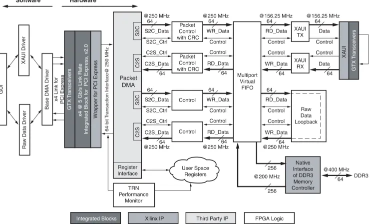
The Virtex-6 FPGA Connectivity TRD features these components: • Virtex-6 FPGA Integrated Block for PCI Express core configured as a
4-lane at 5 Gb/s or 8-lane at 2.5 Gb/s Endpoint for PCI Express, v2.0
• A performance monitor tracks the PCIe® data bandwidth through the transaction interface (TRN) utilization.
• Packet DMA for PCI Express from Northwest Logic, a multichannel DMA that: • Supports full-duplex operation with independent transmit and receive paths • Provides a packetized interface on the backend similar to LocalLink
• Monitors data transfers in the receive and transmit directions • Provides a control plane interface to access user-defined registers • Multiport Virtual FIFO
• The Memory Interface Controller is delivered through the Virtex-6 FPGA Memory Interface Generator (MIG) tool.
X-Ref Target - Figure 1
Figure 1: Block Diagram of the Virtex-6 FPGA Targeted Reference Design
Packet DMA Software Hardware C2 S S 2C C2 S S 2C x4 Link f o r PCI Expre ss
Third Party IP FPGA Logic
64-b it T r a n sa ction Interf a ce@ 250 MHz Register Interface TRN Performance Monitor User Space Registers Packet Control with CRC S2C_Ctrl S2C_Data 64 GTX T r a n s ceiv er s x4 @ 5 G b / s Link R a te Integ r a ted Bloc k f or PCI Expre ss , v2.0 Wr a pper f or PCI Expre ss B as e DMA Dr iv er R a w D a t a Dr iv er XA UI Dr iv er GUI Xilinx IP Integrated Blocks
Native Interface of DDR3 Memory Controller Multiport Virtual FIFO UG372_c1_01_011810 Control WR_Data 64 C2S_Ctrl C2S_Data 64 XAUI TX XA UI GTX T r a n s ceiv er s Control RD_Data 64 Control Data 64 XAUI RX Control WR_Data 64 Control Data 64 @400 MHz @200 MHz @250 MHz @156.25 MHz @250 MHz @250 MHz @250 MHz @250 MHz @156.25 MHz DDR3 64 Control RD_Data 64 Control S2C_Ctrl S2C_Data 64 Control WR_Data 64 Control C2S_Ctrl C2S_Data 64 Raw Data Loopback Control RD_Data 64 Control WR_Data 64 256 256 Control RD_Data 64 Packet Control with CRC
• Software driver for a Linux platform:
• Configures the hardware design parameters • Generates and consumes traffic
• Provides a Graphical User Interface (GUI) to report status and performance statistics
Hardware Demonstration Setup Instructions
This section describes how to set up the hardware demonstration for the Virtex-6 FPGA Connectivity TRD. This demonstration outlines a bridging function between PCIe and XAUI protocols. It also provides accesses to an onboard DDR3 memory.
1. This equipment is needed to run the hardware demonstration: • Virtex-6 FPGA Connectivity Kit
• PC system with a x8 PCIe slot on the motherboard, CD ROM drive, and a USB port
• Monitor, keyboard, and mouse
• Linux Operating System: Fedora 10 LiveCD 2. Run the alternate demonstration.
If there is no access to any of the equipment in step 1, refer to Getting Started with the
Virtex-6 FPGA IBERT Reference Design, page 38 to alternately bring up the ML605
board included in the Virtex-6 FPGA Connectivity Kit. Otherwise, continue with the PCIe to XAUI protocol demonstration in step 3.
3. If the instructions in the Virtex-6 FPGA Connectivity Kit Hardware Setup Guide have already been completed to bring up the Virtex-6 FPGA Connectivity Kit, proceed to
Evaluating the Virtex-6 FPGA Connectivity TRD, page 19; otherwise, continue to
step 4.
4. Hardware Setup I: Board setup and configuration.
The ML605 board is shipped with the FMC Connectivity daughter card attached to the FMC_HPC connector (see Figure 2). To run the Connectivity TRD demonstration, you need to externally loop back the XAUI data through a CX4 loopback connector provided in the connectivity kit.
a. Verify the switch settings are correct:
- Switch S1: 1 = OFF, 2 = OFF, 3 = OFF, 4 = ON
- Switch S2: 1 = ON, 2 = OFF, 3 = OFF, 4 = ON, 5 = ON, 6 = OFF b. Verify that Jumper J42 has pins 3-4 shorted.
X-Ref Target - Figure 2
Figure 2: ML605 and FMC Connectivity Daughter Card
X-Ref Target - Figure 3
UG664_02_022310 Switch S1 J2 J42 Switch S2 CX4 Loopback Connector J2
5. Hardware Setup II: Connect the power connector: a. Turn the PC system off.
b. Connect the 12V ATX power supply’s available 4-pin disk-drive-type power connector of the PC system to the board (J25).
Caution! Using any power supply connector other than the 4-pin inline connector will result in damage to the PC system and the ML605 board.
c. The power switch SW2 should be switched to the ON position (away from the bracket edge of the ML605 board) as shown in Figure 4.
X-Ref Target - Figure 4
Figure 4: 12V ATX Power Supply Connector
UG664_04_022310
J60 SW2 J25
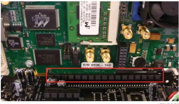
6. Hardware Setup III: Insert the ML605 board into an empty PCIe slot: a. Identify a x8 or a x16 PCIe slot on the PC motherboard.
b. Insert the ML605 board with FMC daughter card and CX4 loopback module in the PCIe slot through the PCIe x8 edge connector.
c. Turn the PC power ON. On power-up, the connectivity targeted reference design for PCIe to XAUI is loaded from the Platform Flash.
7. Configure the desktop PC to boot from the CD ROM:
a. Power the PC system on and watch the initial BIOS screen for a prompt that indicates which key to use for either:
- A boot menu or
- The BIOS setup utility
b. If such a prompt is not visible, refer to the manufacturer’s documentation for the PC system. On many systems, the required key is F12, F2, F1, or Delete.
c. Adjust the boot menu or BIOS boot order settings to make sure that the CD ROM is the first drive in the boot order.
d. Eject the CD ROM bay and insert Fedora 10 LiveCD. e. Save changes and exit the boot menu or BIOS setup. f. The PC system will boot from the CD ROM.
X-Ref Target - Figure 5
Figure 5: Insert the ML605 Board into the PCIe Slot
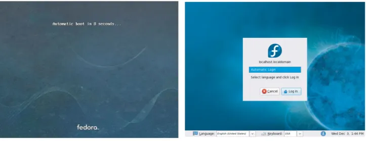
8. Boot Fedora 10 LiveCD and automatically log in:
a. The images in Figure 6 are displayed on power up. Wait two to three minutes, depending on the system configuration.
b. Click Login to enter. Wait one to two minutes, depending on the system configuration.
9. Copy the contents of the USB flash drive:
a. The reference design files are provided on the USB flash drive delivered with the connectivity kit.
b. Insert the USB flash drive into a USB connector of the PC system.
c. Wait for the Fedora 10 operating system to mount the USB flash. When the flash is mounted, an icon pops up on the desktop.
d. Double-click the USB flash drive icon and copy the
v6_pcie_10Gdma_ddr3_xaui folder into the liveuser’s home folder directory. e. Unmount the USB flash. Right-click on the USB flash drive icon and select
Unmount Volume.
X-Ref Target - Figure 6
Figure 6: Fedora Screens
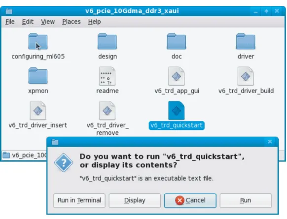
10. Load the driver and launch the Performance Monitor application: a. Navigate to the v6_pcie_10Gdma_ddr3_xauifolder.
b. Double-click v6_trd_quickstart to build the kernel objects, load the device driver, and launch the Performance Monitor application.
c. A window prompt appears as shown in Figure 7. Click Run in Terminal to proceed.
X-Ref Target - Figure 7
Figure 7: Load Driver and Launch Performance Monitor Application
11. Performance Monitor Application: Verify the board status.
a. Click on the System Status tab to verify the status of the ML605 board and the PCIe link (see Figure 8):
- Link Status: Up
This confirms that the PCIe link is up and a PCIe connection is established between the Virtex-6 FPGA Endpoint for PCI Express and the PC
motherboard chipset.
- Link Speed: 5.0 Gbps
This confirms that the PCIe link is operating at line rate speeds per PCI Express, v2.0.
- Link Width: x4
This confirms that the PCIe link is trained as a x4 link.
X-Ref Target - Figure 8
Figure 8: Verify Board Status in the Performance Monitor
12. Performance Monitor Application: Start the data traffic.
a. To enable the XAUI datapath, click Start Test as shown in Figure 9.
This enables the driver to start generating the data traffic for the DMA channel connected to the XAUI path.
b. To enable the raw datapath, click Start Test as shown in Figure 9.
X-Ref Target - Figure 9
Figure 9: Start Data Traffic from the Performance Monitor
13. Performance Monitor Application: In the dialog box shown in Figure 10, verify data throughput and error-free operation:
a. Verify the PCIe throughput.
b. Verify the DMA channel throughput for the XAUI path. c. Verify the DMA channel throughput for the raw datapath.
d. Verify there are no buffer descriptor errors for error-free operation.
Congratulations! The Virtex-6 FPGA Connectivity Kit is now set up. The pre-built connectivity targeted reference design demonstration has been tested, using the built-in block for PCI Express (4-lane 5 GT/s configuration for PCI Express, v2.0), XAUI
LogiCORE IP module, a Virtual FIFO memory controller that interfaces to the onboard DDR3 SODIMM device, and a third-party DMA controller for PCI Express.
X-Ref Target - Figure 10
Figure 10: Verify Error-Free Operation in the Performance Monitor
Evaluating the Virtex-6 FPGA Connectivity TRD
The Virtex-6 FPGA Connectivity TRD provides a Performance and Status monitor application and GUI. The application enables customers to evaluate different system parameter optimizations. This section demonstrates key performance criteria for the PCI Express, XAUI, and Raw Data Path (Memory) interfaces.
To evaluate the Virtex-6 FPGA Connectivity TRD:
1. Launch the Performance Monitor for the Virtex-6 FPGA Connectivity TRD: a. Navigate to the v6_pcie_10Gdma_ddr3_xaui folder.
b. Double-click v6_trd_quickstart to launch the Performance Monitor and Status GUI.
c. A window prompt appears as shown in Figure 12. Click Run in Terminal to proceed.
X-Ref Target - Figure 11
Figure 11: Launch the Performance Monitor and Status GUI
X-Ref Target - Figure 12
2. Set up the test in the Performance Monitor: a. Two Data Transmission options are provided:
- XAUI Path
- Raw Data Path (DDR3)
b. These Packet Size options are provided:
- XAUI Path
Minimum Packet Size: Choose a value between 128 - 16384 Maximum Packet Size: Choose a value between 128 - 16384
- Raw Data Path
Minimum Packet Size: Choose a value between 128 - 16384 Maximum Packet Size: Choose a value between 128 - 16384 3. Execute the test and view payload statistics in Performance Monitor:
a. Click Start Test to start the performance test.
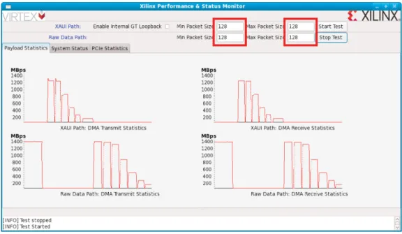
b. View the payload statistics to review data transfers on the XAUI Path and Raw Data Path channels of the DMA engine (see Figure 13).
X-Ref Target - Figure 13
Figure 13: Payload Statistics
c. Modify the Packet Size parameters for the XAUI Path and Raw Data Path transfers (see Figure 14). Then view the payload statistics to review data transfers on the XAUI Path and Raw Data Path channels of the DMA engine.
4. View the PCIe statistics in Performance Monitor (see Figure 15). Click PCIe Statistics to view data transfer numbers on the PCIe interface.
X-Ref Target - Figure 14
Figure 14: Packet Size Field in the Payload Statistics Tab
X-Ref Target - Figure 15
Congratulations! The system performance of the Virtex-6 FPGA Connectivity Kit has been evaluated using the pre-built demonstration design. This design includes the built-in integrated block for PCI Express (4-lane, 5 GT/s configuration for PCI Express v2.0), XAUI LogiCORE IP, a Virtual FIFO memory controller designed to interface to the onboard DDR3 SODIMM device, and a third-party DMA controller for PCI Express.
Installation and Licensing of ISE Design Suite 11
This Virtex-6 FPGA Connectivity Kit comes with an entitlement to a full seat of the ISE Design Suite: Embedded Edition that is device locked to a Virtex-6 LX240T FPGA. This software can be installed from the DVD or the Web installer can be downloaded from
http://www.xilinx.com/support/download/index.htm.
The ISE 11.1 software must be loaded first followed by the ISE 11.4 software update.
ISE 11.1 Software Installation
To install the ISE 11.1 software:
1. Run the ISE Design Suite 11 Installer:
a. Option 1: Insert the ISE Design Suite 11 DVD included in this kit into the computer. If the Installer does not start automatically, run the xsetup executable from the DVD.
b. Option 2: Run the Web Installer that can be downloaded from
http://www.xilinx.com/support/download/index.htm
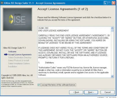
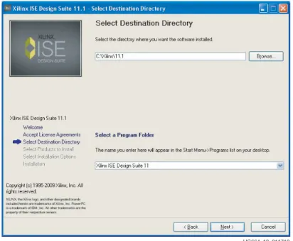
Multiple screens with prompts will be displayed: a Welcome dialog (Figure 16), two License agreements (Figure 17 and Figure 18), and the selection of where to install the software (Figure 19).
Note: The installation only completes successfully when the two license agreements are accepted as well as the default install location.
X-Ref Target - Figure 17
Figure 17: ISE Software End-User License Agreement
X-Ref Target - Figure 18
Figure 18: ISE Software Third- Party Usage License Agreement
UG664_17_011710
2. Click the ISE Design Suite Product radio button in the Select Products to Install dialog window. Make sure that the ISE Design Tools, Embedded Development Kit (EDK), and ChipScope Pro tool are all selected for installation as shown in Figure 20. Click Next.
X-Ref Target - Figure 19
Figure 19: ISE Software Destination Directory
X-Ref Target - Figure 20
4. Near the end of the installation, the dialog shown in Figure 21 appears. Click OK.
5. Click Yes to accept the License Agreement for the Microsoft Visual C++ Redistributable Libraries. The Xilinx ISE tools use the Microsoft Visual C++ Redistributable tools.
6. Cancel out of the Xilinx Update dialog shown in Figure 23, because the ISE 11.4 software update is installed from the 11.4 Update DVD.
X-Ref Target - Figure 21
Figure 21: DSP Post-Installation Dialog
X-Ref Target - Figure 22
Figure 22: Microsoft Visual C++ Library Install
X-Ref Target - Figure 23
UG664_21_011710
7. Click Close to exit the Xilinx License Configuration Manager. The license for the software is acquired after the 11.4 update is installed.
8. Exit the installation.
ISE 11.4 Software Update Installation
Do not install the ISE 11.4 software update from the web; instead use the ISE 11.4 Update DVD included in the kit.
1. Insert the Xilinx ISE Design Suite 11.4 Update DVD included in this kit into the computer.
If the Installer does not start automatically, run the xsetup executable from the DVD. 2. Follow the steps presented by the 11.4 update installer. The update must be installed in
the default directory as shown in Figure 24.
Note: This update will not install correctly if disk space is limited. The 11.4 update is approximately
3GB, and approximately 10 GB disk space is needed to complete the installation. Refer to Answer
Record 32488 to determine disk space requirements. Ensure that adequate disk space is available
prior to beginning installation.
3. Click Continue if the dialog box in Figure 25 appears.
X-Ref Target - Figure 24
Figure 24: Update Install Destination Directory
X-Ref Target - Figure 25
4. Select all update options as shown in Figure 26 and click OK. All updates are needed because they are used by ISE Design Suite: Embedded Edition or are required for Virtex-6 FPGA support.
Note: The ISE 11.4 software update takes from 1 to 3 hours to install.
5. If the dialog in Figure 27 appears, ignore it and click OK.
6. Click OK to exit the installer when the installation has completed (see Figure 28).
X-Ref Target - Figure 26
Figure 26: Available Updates
X-Ref Target - Figure 27
Figure 27: File fileset.txt
X-Ref Target - Figure 28
UG664_26_011710
Downloading and Installing Tool Licenses
1. Visit the Xilinx software registration and entitlement site at
http://www.xilinx.com/getproduct to access the Xilinx product download and
licensing site (Figure 29).
2. Log in to an existing account or create a new account, if needed.
Note: The user name and password are provided in an email sent when the kit was ordered. If this e-mail is unavailable, contact Xilinx customer service for access to the account at
http://www.xilinx.com/support/techsup/tappinfo.htm.
3. After logging in, verify the shipping address, if prompted. Click Next after the shipping address has been verified or updated.
X-Ref Target - Figure 29
Figure 29: Sign In to Xilinx Product Download and Licensing Site
4. Check the ISE Design Suite Embedded Virtex-6 LX240T Device Locked Edition product box and click Generate Node-Locked License as shown in Figure 30.
X-Ref Target - Figure 30
Figure 30: Xilinx Entitlement Center
5. Follow the instructions to generate the license by providing the Host OS information and Host ID (Disk Serial number or Ethernet MAC address) as shown in Figure 31. Click Next.
Note: Laptop users might want to select their Disk ID or Wireless Ethernet card Host ID. Laptops on docking stations might have three Ethernet Host IDs from which to choose. If a docking station Host ID is selected, then the license is available only when docked. It is best to avoid the Host ID of the RJ45 Ethernet connection on laptop computers, because some Ethernet adapters power down when not plugged into the network. To select an Ethernet adapter, it is best to select the wireless card.
X-Ref Target - Figure 31
Figure 31: Selecting the Host ID
6. Review the license request as shown in Figure 32 and click Next.
7. The generated license is e-mailed to the user in an e-mail similar to the one shown in
Figure 33.
X-Ref Target - Figure 32
Figure 32: Reviewing the License Request
X-Ref Target - Figure 33
Figure 33: Xilinx License Notification E-mail
UG664_32_011710
8. Start the Xilinx License Manager (Start→ Programs→ ISE Design Suite 11→ Manage Xilinx Licenses) and click Copy License to install the license on the computer.
9. Navigate to the Xilinx.lic file location and select it (see Figure 35).
X-Ref Target - Figure 34
Figure 34: Manage Xilinx License Tab
X-Ref Target - Figure 35
10. The ISE software license has been successfully installed. Click OK on the Success Dialog (Figure 36) and close the Xilinx License Configuration Manager.
Congratulations! The ISE Design Suite 11 tools are now installed and the licenses are set up for the Embedded Edition of the tools. For detailed information on licensing and
installation, refer to:
http://www.xilinx.com/support/documentation/sw_manuals/xilinx11/irn.pdf
The Connectivity Design is Ready for Modification
Now that the FPGA-based connectivity demonstration has been set up and evaluated and the ISE Design Suite Logic plus Embedded Edition is completely installed, the connectivity design for the Virtex-6 LX240T FPGA can be modified. This step enables the designer to understand the simplified flow of the Xilinx tools and design methodologies as they apply to the Virtex-6 FPGA Connectivity Kit and the Virtex-6 FPGA Connectivity Targeted Reference Design.
X-Ref Target - Figure 36
Figure 36: License Installation Successful
Modifying the Virtex-6 FPGA Targeted Reference Design
This section describes how to modify the design:• Hardware and RTL modifications • Software and driver modifications
Hardware Modifications
This section describes how the hardware is modified. This exercise modifies the PCI Express vendor ID.
To make RTL design changes and implement the design, follow these steps: 1. Use the PC system or laptop on which the Xilinx design tools were installed. 2. Copy the contents of the included USB stick into a local directory on this machine. 3. Make design changes:
a. Navigate to the v6_pcie_10Gdma_ddr3_xaui/design/source/ directory. b. Edit the v6_pcie_10Gdma_ddr3_xaui.v file.
c. Search for this string: VENDOR_ID.
d. Change the alphanumeric value 10EE on this line to the vendor ID assigned to the user’s company by PCI-SIG (e.g., the vendor ID for Xilinx is 10EE). Change this value to 19AA.
e. Save changes and exit.
4. Generate the MIG IP core required for the Targeted Reference Design with the appropriate configuration:
a. Open a command or a terminal window.
b. Navigate to the v6_pcie_10Gdma_ddr3_xaui/design/ip_cores/mig directory.
c. Execute this command at the command line:
$ coregen -b mig_33.xco
Wait for this command to complete before proceeding. 5. Build and implement the design:
a. Open a terminal window.
b. Navigate to the v6_pcie_10Gdma_ddr3_xaui/design/implement/ directory.
6. Program the FPGA:
a. If the ML605 board is still plugged into the PC system, shut down the PC system and remove the ML605 board.
b. To program the FPGA using Platform Flash, refer to the jumper settings detailed in
step 4 of Hardware Demonstration Setup Instructions, page 10.
c. For all other ML605 switch and jumper settings, keep them at the factory default configuration as indicated in UG534, ML605 Hardware User Guide.
7. Set up the board:
a. Connect the mini USB cable to the USB-JTAG connector as shown in Figure 37. The other end of the USB cable is connected to the PC system or laptop on which the Xilinx design tools were installed.
b. Power off the ML605 board (the power switch should be towards the bracket edge). Use the included wall power adapter to provide 12V power to the 6-pin connector. Power on the ML605 board.
X-Ref Target - Figure 37
Figure 37: Setting Up the Board
8. Program the onboard Platform Flash: a. Open a terminal window.
b. Navigate to the v6_pcie_10Gdma_ddr3_xaui/design/implement/ results_x4_gen2_240t directory.
c. Execute the FPGA programming script at the command prompt. This operation takes approximately 600 to 800 seconds to complete.
- $ impact -batch ml605program.cmd (for Linux based machines)
- Double-click ml605program.bat (for Windows based machines) d. A command shell is opened. After successful completion, the Programmed
successfully message should appear.
e. Turn off the power switch and remove the power connector. f. Carefully remove the mini USB cable.
The Virtex-6 FPGA Connectivity TRD is now modified and programmed into the Platform Flash and will automatically configure at power up.
Test Setup
X-Ref Target - Figure 38
Figure 38: Programming Was Successful
Software Modifications
This section describes how to modify the software. This exercise modifies the PCI Express vendor ID.
To make software design changes, follow these steps:
1. Use the PC system on which the ML605 evaluation board is installed.
2. Copy the contents of the included USB stick into a local directory on this machine: a. Navigate to the v6_pcie_10Gdma_ddr3_xaui/driver/xdma/ directory. b. Edit the xdma_base.c file.
c. Search for this string: #define PCI_VENDOR_ID_DMA.
- Change the alphanumeric value 10EE found on this line, with the vendor ID assigned to the user’s company by PCI-SIG (e.g., the vendor ID for Xilinx is 10EE). Change this value to 19AA.
- Save the changes and exit.
3. Load the driver and launch the Performance Monitor application: a. Navigate to the v6_pcie_dma_ddr3_xaui folder.
b. Double-click v6_trd_quickstart.
This step builds kernel objects, loads the device driver, and launches the Performance Monitor application.
c. Click Run in Terminal to proceed.
4. Follow step 11, page 16 through step 13, page 18 in Hardware Demonstration Setup Instructions to completely verify the modified settings.
5. Follow step 1, page 19 through step 4, page 21 in Evaluating the Virtex-6 FPGA
Connectivity TRD to evaluate the performance for the modified design.
6. Review the system status. Click System Status to review:
• PCIe link status, Vendor ID, and Device ID information.
• The vendor ID status displayed on this screen. It should be equal to 19AA, corresponding to the hardware change that was performed.
Congratulations! The Virtex-6 FPGA Connectivity Kit using the connectivity TRD has been fully set up, and the system performance has been evaluated. The Xilinx design flow has been reviewed for modifying the connectivity TRD. This design includes the built-in integrated block for PCI Express (4-lane, 5 GT/s configuration for PCI Express v2.0), XAUI LogiCORE IP, a Virtual FIFO memory controller designed to interface to the onboard DDR3 SODIMM device, and a third-party DMA controller for PCI Express.
Getting Started with the Virtex-6 FPGA IBERT Reference Design
This Virtex-6 FPGA Connectivity Kit comes with an Integrated Bit Error Ratio Test (IBERT) reference design available on the CompactFlash. The demonstration shows the capabilities of the Virtex-6 LXT device using the GTX transceivers running at 3.125 Gb/s line rates. The GTX transceivers can successfully operate at line rates from 750 Mb/s to 6.6 Gb/s.The Virtex-6 FPGA IBERT reference design has these components: • Virtex-6 FPGA GTX transceivers running at 3.125 Gb/s
• The IBERT v2.0 reference design available through the CORE Generator tool for IP delivery
The design also includes a pseudo-random bit sequence (PRBS) pattern generator and checker.
• Four GTX transceivers in the Virtex-6 LX240T FPGA are accessed through these channels in the IBERT reference design:
• SMA (two channels) • SATA (two channels)
Note: The demonstration is for SMA and SATA external loopback scenarios only.
IBERT Hardware Demonstration Setup Instructions
This section describes how to set up the hardware for the IBERT reference design
demonstration. The IBERT reference design is provided as an FPGA programming file on the CompactFlash.
1. This equipment is needed to run the demonstration: • Virtex-6 FPGA Connectivity Kit
• PC system with USB port • Monitor, keyboard, and mouse
2. Board Setup I – Install the CompactFlash on the ML605 board: Use the CompactFlash provided in the kit (see Figure 39).
3. Board Setup II – Configure the settings for DIP switches S1 and S2 to load the IBERT design from the CompactFlash (see Figure 40), where X = Don’t care, 1 = ON, 0 = OFF): a. Set S1 to 1110 (Position 4 is the most-significant bit, and Position 1 is the
least-significant bit).
b. Set S2 to 0101XX (Position 6 is the most-significant bit, and Position 1 is the least-significant bit).
X-Ref Target - Figure 39
Figure 39: Installing the Included CompactFlash on the ML605 Board
X-Ref Target - Figure 40
4. Board Setup III – Connect a USB cable to the ML605 board as shown in Figure 41: a. Connect the included USB Type-A to Mini-B cable to the USB JTAG connector on
the ML605 board.
b. Connect the other end of this cable to the PC system.
5. Board Setup IV – Use the SMA cables to loop back the transceiver channel pinned to the SMA on the FMC card:
a. Connect J4 to J10 (see Figure 42).
X-Ref Target - Figure 41
Figure 41: Connecting the USB Cable to the USB-JTAG Connector of the ML605
Board
X-Ref Target - Figure 42
b. Connect J6 to J8 (see Figure 43).
c. Connect J3 to J9 (see Figure 44).
X-Ref Target - Figure 43
Figure 43: Configuring the SMA Transceiver Channel with External Loopback - II
X-Ref Target - Figure 44
Figure 44: Configuring the SMA Transceiver Channel with External Loopback - III
UG664_43_021810
d. Connect J5 to J7 (see Figure 45).
e. Connect J11 to J12 with a SATA loopback cable included in the Virtex-6 FPGA Connectivity Kit (see Figure 46).
X-Ref Target - Figure 45
Figure 45: Configuring the SMA Transceiver Channel with External Loopback - IV
X-Ref Target - Figure 46
6. Board Setup V – Connect the power connector:
a. Using the included power supply, connect the power supply connector to the ML605 board as shown in Figure 47.
b. The power switch SW2 should be switched to the ON position.
X-Ref Target - Figure 47
Figure 47: Powering Up the ML605 Board
7. Board Setup VI – Load the FPGA with the IBERT design from the CompactFlash: a. Press switch SW3 to configure from the CompactFlash.
b. Verify that the FPGA is loaded with the IBERT design. The DONE LED should be lit.
8. The IBERT Reference Design files are provided on a USB flash drive delivered as a part of the kit. Copy the contents of the included USB flash drive:
a. Insert the USB flash drive into a USB connector of the PC system.
b. Wait for the operating system to mount the USB flash. When the flash is mounted, an icon pops up on the desktop.
c. Navigate to the USB flash drive and copy the
X-Ref Target - Figure 48
Figure 48: FPGA Programmed with the IBERT Reference Design
9. Open the ChipScope Pro Analyzer window:
a. Click on Programs→ Xilinx ISE Design Suite→ ChipScope Pro→ Analyzer. b. Click on Open Cable Button as shown in Figure 49.
10. Open the ChipScope Pro Analyzer project (see Figure 50): a. Click File→ Open Project.
b. Navigate to the ML605_FMC_XM104_Ibert_Reference_Design folder. c. Select ml605_fmc_xm104_ibert.cpj.
X-Ref Target - Figure 49
Figure 49: Launch the ChipScope Pro Analyzer Window
X-Ref Target - Figure 50
UG664_49_021810
11. Load the ChipScope Pro Analyzer project:
a. Click Yes on the dialog box shown in Figure 51.
12. Load and reset the IBERT reference design through the GUI (see Figure 52). GTX0_113 → FMC Daughter Card connector: DP3 SATA2 Host Channel GTX1_113 → FMC Daughter Card connector: DP2 SATA1 Host Channel GTX2_113 → FMC Daughter Card connector: DP1 SMA Channel GTX3_113 → FMC Daughter Card connector: DP0 SMA Channel
X-Ref Target - Figure 51
Figure 51: Load the ChipScope Tool Project and Communicate with the IBERT
Reference Design
X-Ref Target - Figure 52
13. Verify the line rates for the GTX transceivers (see Figure 53):
a. The line rate is set to 3.125 Gb/s for all four GTX transceiver channels instantiated in the design.
b. The GTX0_113 and GTX1_113 transceiver channels have been looped on external loopback through a SATA cable. Select the loopback mode for these transceiver channels as None (no internal loopback). The GTX2_113 and GTX3_113
transceiver channels have been looped on external loopback through an SMA cable. Select the loopback mode for these transceiver channels as None (no internal loopback).
14. Configure the GTX transmit parameter settings (see Figure 54):
a. Set the TX Diff Output Swing parameter to 590 mV (0110) for the SATA channels and 365 mV for the SMA channels.
b. Set the TX Pre-Emphasis parameter to 0 dB (000).
X-Ref Target - Figure 53
Figure 53: Verify the GTX Transceiver Loopback Configuration and Link Status
X-Ref Target - Figure 54
15. Configure the bit error ratio test (BERT) parameter settings (see Figure 55): a. Set the TX/RX data patterns to PRBS 7-bit and 15-bit.
b. Click the BERT Reset buttons for each channel.
16. View the reported BERT (see Figure 56). The RX bit error count should be 0.
X-Ref Target - Figure 55
Figure 55: Configuring the BERT Settings for the GTX Transceiver Channels
X-Ref Target - Figure 56
Figure 56: Verify the Bit Error Ratio on All Four Transceiver Channels
UG664_55_021810
Reference Design Files
The design checklist in Table 1 includes simulation, implementation, and hardware details for the reference designs. After registration, reference design files are available for download at ug664.zip.
Installation is Complete
Table 1: Design Checklist
Parameter Description General
Developer Name Xilinx
Target devices (stepping level, ES, production, speed grades) XC6VLX240T-1-FF1156
Source code provided Y (for custom logic only)
Source code format Verilog
Design uses code or IP from an existing reference design or application note, third party, CORE Generator software
Uses code from a third party and LogiCORE IP from the CORE Generator software
Simulation
Functional simulation performed Y
Timing simulation performed N
Testbench used for functional and timing simulations Y (for functional simulations)
Testbench format System Verilog (inhouse verification), Verilog (customer deliverable)
Simulator software/version used ModelSim Questa 6.5a (inhouse verification)/ ModelSim 6.4b (out-of-box simulation support)
SPICE/IBIS simulations N
Implementation
Synthesis software tools/version used XST
Implementation software tools/versions used ISE 11.4 tool
Static timing analysis performed Y
Hardware Verification
Hardware verified Y
Hardware platform used for verification ML605 board and FMC X104 Connectivity daughter card
Warranty
THIS LIMITED WARRANTY applies solely to standard hardware development boards and standard hardware programming cables manufactured by or on behalf of Xilinx (“Development Systems”). Subject to the limitations herein, Xilinx warrants that
Development Systems, when delivered by Xilinx or its authorized distributor, for ninety (90) days following the delivery date, will be free from defects in material and
workmanship and will substantially conform to Xilinx publicly available specifications for such products in effect at the time of delivery. This limited warranty excludes:
(i) engineering samples or beta versions of Development Systems (which are provided “AS IS” without warranty); (ii) design defects or errors known as “errata”;
(iii) Development Systems procured through unauthorized third parties; and (iv) Development Systems that have been subject to misuse, mishandling, accident, alteration, neglect, unauthorized repair or installation. Furthermore, this limited warranty shall not apply to the use of covered products in an application or environment that is not within Xilinx specifications or in the event of any act, error, neglect or default of Customer. For any breach by Xilinx of this limited warranty, the exclusive remedy of Customer and the sole liability of Xilinx shall be, at the option of Xilinx, to replace or repair the affected products, or to refund to Customer the price of the affected products. The availability of replacement products is subject to product discontinuation policies at Xilinx. Customer may not return product without first obtaining a customer return material authorization (RMA) number from Xilinx.
THE WARRANTIES SET FORTH HEREIN ARE EXCLUSIVE. XILINX DISCLAIMS ALL OTHER WARRANTIES, WHETHER EXPRESS, IMPLIED OR STATUTORY, INCLUDING, WITHOUT LIMITATION, ANY WARRANTY OF MERCHANTABILITY, FITNESS FOR A PARTICULAR PURPOSE, OR NON-INFRINGEMENT, AND ANY WARRANTY THAT MAY ARISE FROM COURSE OF DEALING, COURSE OF PERFORMANCE, OR USAGE OF TRADE. (2008.10)
Do not throw Xilinx products marked with the “crossed out wheelie bin” in the trash. Directive 2002/96/EC on waste electrical and electronic equipment (WEEE) requires the separate collection of WEEE. Your cooperation is essential in ensuring the proper management of WEEE and the protection of the environment and human health from