Electronic effects of defects in one-dimensional channels
Elliot J. Fuller, Deng Pan, Brad L. Corso, O. Tolga Gul, and Philip G. Collins
Dept. of Physics and Astronomy, University of California at Irvine, Irvine CA USA 92697
ABSTRACT
As electronic devices shrink to the one-dimensional limit, unusual device physics can result, even at room temperature. Nanoscale conductors like single-walled carbon nanotubes (SWNTs) are particularly useful tools for experimentally investigating these effects. Our characterization of point defects in SWNTs has focused on these electronic consequences. A single scattering site in an otherwise quasi-ballistic SWNT introduces resistance, transconductance, and chemical sensitivity, and here we investigate these contributions using a combination of transport and scanning probe techniques. The transport measurements determine the two-terminal contributions over a wide range of bias, temperature, and environmental conditions, while the scanning probe work provides complementary confirmation that the effects originate at a particular site along the conduction path in a SWNT. Together, the combination proves that single point defects behave like scattering barriers having Poole-Frenkel transport characteristics. The Poole-Frenkel barriers have heights of 10 – 30 meV and gate-dependent widths that grow as large as 1 m due to the uniquely poor screening in one dimension. Poole-Frenkel characteristics suggest that the barriers contain at least one localized electronic state, and that this state primarily contributes to conduction under high bias or high temperature conditions. Because these localized states vary from one device to another, we hypothesize that each might be unique to a particular defect’s chemical type.
Keywords: carbon nanotube, defect scattering, Poole-Frenkel conduction, Kelvin probe force microscopy, scanning gate microscopy, electronic spectroscopy
1.
INTRODUCTION
Single-walled carbon nanotubes (SWNTs) provide a unique electronic system for investigating transport in the quasi-one dimensional limit.1 Even more than with other novel systems like graphene or nanowires, SWNTs confine carriers to an
extreme limit where quantum effects can dominate all the way up to room temperature.
A typical SWNT has a diameter of 1 to 2 nm and a conductive outer surface that derives from the pzorbitals of the sp2 carbon sheet. Electronic subbands in a SWNT are separated by more than 0.5 eV, so that under moderate conditions only the lowest energy bands contribute to transport. Degeneracy at the Fermi level includes two, spin-degenerate bands, but the interactions between them are particularly weak,2-4 so that the SWNT is very nearly a one-dimensional
system.
In this one-dimensional limit, disorder becomes increasingly important. A single lattice defect or other type of scattering site can have tremendous consequence to physical and chemical properties, including electronic characteristics.5 In
SWNTs, this importance was predicted in early theoretical work6-11 and then expanded upon as experimentalists became
more adept at controlling SWNT surface chemistry12, 13 and observing the effects electronically.14, 15 This body of work
provided a solid foundation for rapid progress understanding defect scattering in graphene,16, 17 but today the field is
returning to investigations of the more novel, highly sensitive, one-dimensional case of SWNTs.
One experimental barrier to the study of SWNT defects has been the problem of controlled defect production. Various groups have observed damage from mechanical treatments, electron beams, and ion irradiation, but in most cases the nature and quantity of damage can be difficult to determine.18-21 Consequently, we have developed experimental
techniques for intentionally introducing a single defect into a SWNT in a field-effect transistor (FET) device geometry.22
Using these techniques, one particular SWNT can be studied before and after defect incorporation, and defects of known chemistries can be characterized and compared.23, 24 Here, we focus on point defects introduced by electrochemical
oxidation in water, which tends to covalently add hydroxyl groups to the carbon lattice in ways that can be directly compared to theoretical calculations.25, 26 Detailed, specific techniques for sample preparation and defect incorporation
2.
SCANNING PROBE MICROSCOPY OF DEFECT SITES
Scanning probe microscopy (SPM) provides a wide range of information about nanoscale electronic devices. When extended beyond simple topographic imaging, SPM can provide local information about electronic, chemical, magnetic and other physical properties. Combined with traditional transport measurements, these imaging modes produce spatially resolved spectroscopic data sets capable of identifying discrete electronic levels. Although electronic states are imaged directly by tunneling spectroscopy, that technique is not particularly applicable to devices fabricated on gate oxides like SWNT FETs. Instead, we primarily rely on two SPM techniques suited for gate oxides to investigate SWNT defect sites: Kelvin probe force microscopy (KPFM) and scanning gate microscopy (SGM).
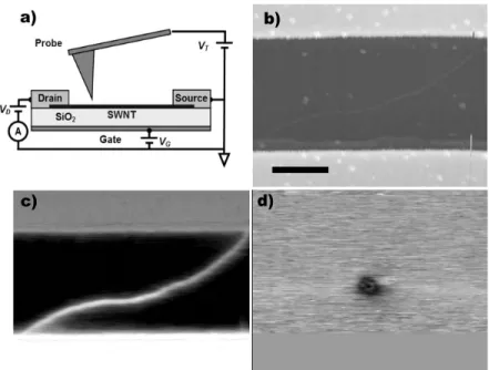
Figure 1. Scanning probe microscopy of individual SWNTs. (a) Schematic of a conductive-tip atomic force microscope probing a typical, three-terminal SWNT FET device. (b) Topography of an example device, with source and drain electrodes across the top and bottom of the image and the SWNT laying diagonally. Scale bar is 1 m. (c) KPFM image of electrostatic potentials in the same device with a source-drain bias of 1.0 V. Line cuts along the SWNT can determine the diffusive scattering length and identify scattering sites with anomalous potential drops. (d) SGM images of the same SWNT identify sensitivity to gating by the AFM probe. For a SWNT with a relatively insensitive, metallic bandstructure as shown here, nearly all of the device’s gate sensitivity can be concentrated at a defect site.
2.1 Kelvin Probe Force Microscopy (KPFM)
KPFM directly images the surface potential of nanoscale materials. The technique relies upon electrostatic deflection of the AFM probe by the sample. Using a feedback loop to drive the probe potential VT to minimize the electrostatic forces, KPFM determines the local contact potential everywhere on a surface. Recently, we described a frequency-modulated KPFM technique that yields quantitative information about localized resistance in nanoscale current carrying devices, and the application of that technique to measuring electronic mean free paths.27 Using images like the example
in Fig. 1c, line cuts clearly show the drop in potential along a SWNT determine the diffusive scattering lengths. In addition, a SWNT with a defect or other prominent scattering site will exhibit additional KPFM gradients. While not apparent in the two dimensional image of Fig. 1c, these features are more evident in line cuts along the SWNT.
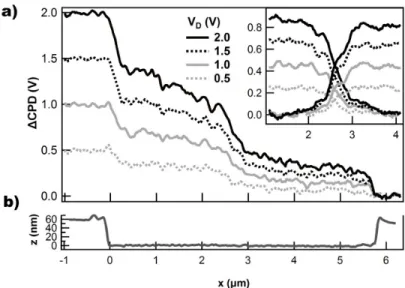
Fig. 2 provides one-dimensional data of the KPFM potential along the SWNT (Fig. 2a) and the device’s topographic height (Fig. 2b), shown primarily to indicate the location of source and drain electrodes. Fig. 2a shows line cuts at applied biases ranging from 0.50 to 2.0 V. Sharp potential drops at x = 0 and x = 5.8 m align with the electrode positions. While some of each drop is associated with contact resistance, the stronger contribution is a change in probe coupling to the electrodes and back gate as the probe moves across the device. As described previously, this change in coupling obscures electrostatic effects in the immediate vicinity of the electrode edges.27
Figure 2. KPFM potential maps along SWNTs. (a) Contact potential difference along a current-carrying SWNT at different biases as shown. The inset shows complementary measurements at smaller biases and with the bias reversed. (b) Device topography indicates the spatial positions of source and drain electrodes.
Far from the source and drain electrodes, variations in potential truly reflect dissipation along the SWNT channel. For biases below 0.5 V, the potential is relatively flat except for a drop centered around x = 2.7 m. At low biases, dissipation by this defect in the middle of the SWNT channel dominates the total resistance. Using a combination of forward and reverse bias (Fig. 2a, inset), we clearly identify a central point around which the potential drop is symmetric. We also note that the potential drops over a constant length of ~1 m. In similar measurements on 5 different devices, characteristic lengths varied from 0.3 – 1.0 m, with additional variation due to gating.
At higher biases, the slope dV/dx increases as diffusive scattering throughout the channel length contributes to the total resistance. Even at the highest bias of 2.0 V, however, the additional potential drop in the vicinity of the defect site remains and can be quantitatively separated from the underlying, diffusive gradient. In all of the curves of Fig. 2a, a zero-bias measurement has been subtracted to remove artifacts from static point charges on the SiO2 and emphasize the
dissipative portion that is proportional to current flow.
SWNT are extremely poor at screening charge due to their one-dimensional geometry and low carrier density.28, 29
Consequently, the depletion length surrounding a barrier can extend many hundreds of nm, consistent with the lengths measured here by KPFM. Similar effects are observed in SWNT p-n junctions under low doping concentrations.30
Consequently, we model electrochemically-produced point defects as single, localized barriers surrounded by extended depletion region with screening lengths of hundreds of nm.
2.2 Scanning Gate Microscopy (SGM)
In addition to the local information determined by KPFM, point scattering sites can be locally gated by the AFM probe to determine their gate sensitivity and contribution to device transconductance dG/dVg. An example image is shown in Fig. 1d. The SGM technique directly measures dG/dVg, and it can be extended to acquire SGM images as a function of back gate and tip biases.23 This SGM technique, called scanning gate spectroscopy (SGS), allows a combination of
spatial and energetic resolution of dG/dVg at each point along a SWNT.
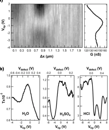
An example SGS image, shown in Fig. 3a, maps the SWNT response in grayscale to a probe tip sweeping from -4 to 2 V as it moves to each point along the SWNT from source to drain. The image is almost entirely uniform except for two features. First, a weak feature close to x = 0 corresponds to the gate sensitivity of a Schottky barrier at the SWNT-electrode interface. A much stronger feature centered around x = 0.75 corresponds to a SWNT defect site. Here, we observe a conductance maximum at Vtip = -1 V, with a decrease in conductance to either side. A vertical cut through the data at the site of the defect (x = 0.8 m) is shown to the right. This curve depicts the device conductance as a function
of the tip’s local gating of the defect site, and it allows us to calculate a transmission function for the defect. Note that the asymmetry versus tip gating suggests a barrier for hole conduction that is monotonically repulsive for Vtip > -1 V but which has attractive well when Vtip < -1 V.
Figure 3. SGS maps of transconductance around a defect site in a SWNT. (a) Device conductance, plotted on a grey scale, as a function of the AFM tip position x and bias Vtip. Far from either electrode, a defect at x = 0.8 m introduces a gate sensitivity. A line cut through the SGS image at this position is shown to the right. (b) The same curve, converted into an effective transmission function T, illustrates the contribution of this particular defect to the device resistance. Changing the oxidation electrolyte leads to other transmission functions as shown.
In contrast to traditional semiconductor defects, a SWNT defect can have a large number of different chemistries and, consequently, scattering potentials. Experimentally, we control the defect chemistry on a particular SWNT device by performing point functionalization in different electrolytes, effectively adding different types of covalent adducts to SWNT sidewalls.22 Subsequently, we have observed different transmission functions following point oxidation in H
2O,
H2SO4, and HCl. Fig. 3b compares SGS transmission functions measured for these three types of oxidation, as
performed on three different SWNT devices. Note that for all three examples, the transmission function has a maximum at which we define the energy barrier to be transparent (Vdefect= 0 V). The figure suggests how the SGS technique can
be used to distinguish different types of scattering sites, especially when amplified by the extreme electronic sensitivity of one-dimensional conduction. The unique opportunities of mapping correspondences between chemical structure and electronic transport and comparing experiment with first-principles calculations makes the SGS technique very promising for continued work.
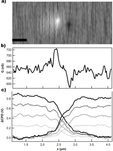
Most SWNT defects exhibit a single, spatially symmetric scattering site that has a transmission maximum at one bias, like those depicted in Fig. 3b. However, some defects have more complex SGM images and SGS spectra. The most frequent variation we have observed is a dipole-like defect that is electrostatically asymmetric around a center point. For example, Fig. 4a shows a higher resolution inspection of the defect discussed in Figs. 1 and 2. Instead of a circularly symmetric maximum, this defect exhibits a conductance a maximum and a minimum offset by ~150 nm the center line.
Fig. 4b shows a line cut through the SGM data along the SWNT about the defect site. The KPFM potential profiles from Fig. 2a are plotted again on a shared x–axis to allow straightforward comparisons. The inflection point in the SGS image is aligned with the midpoint of the central potential drops in the KPFM data (Fig. 4c). We attribute the maximum and minimum of gate sensitivity on either side of the defect correspond to the leading and trailing edges of the depletion zones, respectively.
Figure 4. A defect site with a dipole-like structure. (a) SGM images sometimes exhibit asymmetric mirror symmetries around a central point. (b) A line cut through the SGM image clearly depicts the bipolar electrostatic response of the defect. (c) KPFM data from Fig. 2a are reproduced here on a shared x–axis to indicate how the SGM extrema align with drops in potential. Under both forward and reverse bias, the SGM extrema indicate the edges of the region with steepest potential gradient dV/dx.
3.
POOLE-FRENKEL TRANSPORT
The Poole-Frenkel model of conduction describes defect-assisted conduction through thin insulating films.31, 32 In a
Poole-Frenkel system, electrons tunnel into localized states in the insulating film and are then cross the remaining barrier by Schottky emission. Eq. 1 depicts the characteristic temperature and bias dependence of Poole-Frenkel conduction, where a, b, c and d are all positive constants. Fitting the parameters d and c to experimental data uniquely determines the insulating film width and the barrier height of traps within the film, respectively.
I
(
V
,
T
)
aV
exp[(
b
(
V d
)
1/2
c
) /
kT
]
(1)Previously, conduction through heavily damaged SWNTs has been found to result in I(V,T) characteristics that have the same bias and temperature dependence as bulk Poole-Frenkel conduction.33-35 Here, we show that an individual defect
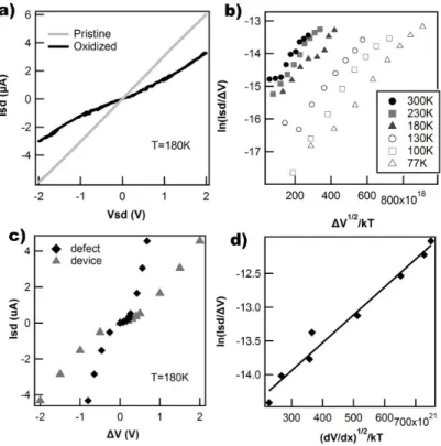
site exhibits the same features. Fig. 5a shows two I(V) curves from the same SWNT FET before and after electrochemical point functionalization has introduced a point defect. The defect introduces a strong, nonlinear bias dependence to the I(V). Plots of ln(I/V) vs. V1/2/T produce a family of straight-line curves (Fig. 5b) indicating that the
new bias- and temperature-dependences are well fit by the bulk Poole-Frenkel model.
While Eq. 1 provides a satisfactory fit to the data, this bulk model may not be appropriate to the one-dimensional electrostatics of the SWNT. For instance, the extracted parameters determine the Poole-Frenkel barriers to have heights of 10 to 30 meV but barrier widths of 300 to 1000 nm. In the bulk model, this width is the physical thickness of the insulating film, across which an applied bias produces a constant electric field. In the SWNT experiment, the width of the defect cannot extend 300 to 1000 nm. Instead, the defect is believed to have a physical extent no larger than 10 nm. KPFM resolves this discrepancy by directly imaging the potential profiles along a SWNT. In fact, the potential does drop over distances as large as 1000 nm, but the width is understood to be a depletion effect.28, 29 The SWNT depletion
regions, and not the physical defect itself, extends for 100’s of nm and governs the magnitude of the electric field in the Poole-Frenkel model.
To support this argument, potential drops V have been extracted from KPFM line profiles. Plots of I(V) have the same shape and characteristics as the two-terminal measurements (Fig. 5c), but explicitly exclude the additional potential drops caused by contact resistance and diffusive scattering along the pristine SWNT sections. Plotting the KPFM data on axes of ln(I/V) and V1/2/T indicates that Eq. 1 provides an excellent fit (Fig. 5d) to the portion of the potential drop
associated with the defect site.
Figure 5. Poole-Frenkel characterization of a SWNT device. (a) I(V) characteristics of the same SWNT before and after electrochemical introduction of a defect. (b) Poole-Frenkel plots of similar I(V) curves at 6 different temperatures. (c) The I(V) curve from transport overlaid by the effective I(V) determined from KPFM. The transport measurement (grey) includes contact and diffusive resistances and therefore overstates the potential drop V. (d) A Poole-Frenkel plot of data from the KPFM potential profiles in Fig. 2.
We typically find that the two-terminal transport and KPFM measurements give similar Poole-Frenkel barrier parameters at low bias, where resistance is predominantly due to the defect. However, device-to-device variation suggests that other parameters may also be important. For example, preliminary three-terminal measurements reveal that
the defect barrier height and width are sensitive to the back gate electrode. This is consistent with SGS measurements described above, which demonstrate that trapping by a state can be in- or out-of-resonance. A gate-dependent barrier width is also in agreement with the depletion interpretation, since the depletion length in observed by KPFM should be strongly dependent on the SWNT’s carrier density.
4.
CONCLUSION
One-dimensional conductors provide unique access for multi-terminal transport measurements to be compared with scanning probe characterization. In the case of scattering by SWNT defects, scanning probe measurements reveal the cause of complex bias, gating, and temperature dependences in the transport data. By interrogating single defects with the KPFM, SGM, and SGS modes, the precise scattering by particular SWNT defect site can be studied in detail. Since the measurements reveal discrete electronic states, further work might successfully associate specific features with particular types of chemical disorder.
REFERENCES
[1] M. J. Biercuk, S. Ilani, C. M. Marcus et al., [Electrical transport in single-wall carbon nanotubes] Springer-Verlag, Berlin(2008).
[2] W. Liang, M. Bockrath, D. Bozovic et al., “Fabry-Perot interference in a nanotube electron waveguide,” Nature, 411(6838), 665-9 (2001).
[3] W. Liang, M. Bockrath, and H. Park, “Shell filling and exchange coupling in metallic single-walled carbon nanotubes,” Physical Review Letters, 88(12), 126801-4 (2002).
[4] P. L. McEuen, M. Bockrath, D. H. Cobden et al., “Disorder, pseudospins, and backscattering in carbon nanotubes,” Physical Review Letters, 83(24), 5098 (1999).
[5] P. G. Collins, [Defects and disorder in carbon nanotubes] Oxford Univ. Press, Oxford(2010).
[6] H. Ajiki, and T. Ando, “Lattice distortion with spatial variation of carbon nanotubes in magnetic fields,” Journal of the Physical Society of Japan, 65(9), 2976-2986 (1996).
[7] C. Kane, L. Balents, and M. P. A. Fisher, “Coulomb interactions and mesoscopic effects in carbon nanotubes,” Physical Review Letters, 79(25), 5086-9 (1997).
[8] T. Nakanishi, and T. Ando, “Scattering by topological disorder in connected carbon nanotubes in magnetic fields,” Physica B-Condensed Matter, 251, 136-139 (1998).
[9] M. Igami, T. Nakanishi, and T. Ando, “Conductance of carbon nanotubes with a vacancy,” Journal of the Physical Society of Japan, 68(3), 716-719 (1999).
[10]T. Ando, T. Nakanishi, and M. Igami, “Effective-mass theory of carbon nanotubes with vacancy,” Journal of the Physical Society of Japan, 68(12), 3994-4008 (1999).
[11]L. Chico, L. X. Benedict, S. G. Louie et al., “Quantum Conductance of carbon nanotubes with defects,” Physical Review B, 54, 2600 (1996).
[12]S. Niyogi, M. A. Hamon, H. Hu et al., “Chemistry of single-walled carbon nanotubes,” Accounts of Chemical Research, 35(12), 1105-1113 (2002).
[13]M. Burghard, “Electronic and vibrational properties of chemically modified single-wall carbon nanotubes,” Surface Science Reports, 58, 1-109 (2005).
[14]M. Bockrath, W. J. Liang, D. Bozovic et al., “Resonant electron scattering by defects in single-walled carbon nanotubes,” Science, 291(5502), 283-285 (2001).
[15]M. Freitag, A. T. Johnson, S. V. Kalinin et al., “Role of single defects in electronic transport through carbon nanotube field-effect transistors,” Physical Review Letters, 89(21), 216801 (2002).
[16]K. Kim, H. J. Park, B.-C. Woo et al., “Electric Property Evolution of Structurally Defected Multilayer Graphene,” Nano Letters, 8(10), 3092-3096 (2008).
[17]N. Vandecasteele, A. Barreiro, M. Lazzeri et al., “Current-voltage characteristics of graphene devices: Interplay between Zener-Klein tunneling and defects,” Physical Review B, 82(4), 045416 (2010).
[18]A. V. Krasheninnikov, K. Nordlund, and J. Keinonen, “Production of defects in supported carbon nanotubes under ion irradiation,” Physical Review B, 65, 165423 (2002).
[19]J. A. V. Pomoell, A. V. Krasheninnikov, K. Nordlund et al., “Ion ranges and irradiation-induced defects in multiwalled carbon nanotubes,” Journal of Applied Physics, 96(5), 2864-2871 (2004).
[20]V. Skakalova, A. B. Kaiser, Z. Osvath et al., “Ion irradiation effects on conduction in single-wall carbon nanotube networks,” Applied Physics A: Materials Science Processing, 90(4), 597-602 (2008).
[21]V. Skakalova, Y. S. Woo, Z. Osvath et al., “Electron transport in Ar+-irradiated single wall carbon nanotubes,” Physica Status Solidi B-Basic Solid State Physics, 243(13), 3346-3350 (2006).
[22]B. R. Goldsmith, J. G. Coroneus, V. R. Khalap et al., “Conductance-controlled point functionalization of single-walled carbon nanotubes,” Science, 315, 77-81 (2007).
[23]S. R. Hunt, D. Wan, V. R. Khalap et al., “Scanning Gate Spectroscopy and Its Application to Carbon Nanotube Defects,” Nano Letters, 11, 1055-60 (2011).
[24]S. R. Hunt, E. J. Fuller, B. L. Corso et al., “Distinguishing carbon nanotube defect chemistry using scanning gate spectroscopy,” Physical Review B, 85(23), 235418 (2012).
[25]M. K. Ashraf, N. A. Bruque, R. R. Pandey et al., “Effect of localized oxygen functionalization on the conductance of metallic carbon nanotubes,” Physical Review B, 79(11), 115428 (2009).
[26]Y. Kanai, V. R. Khalap, P. G. Collins et al., “Atomistic Oxidation of a Carbon Nanotube in Nitric Acid,” Physical Review Letters, 104, 066401 (2010).
[27]E. J. Fuller, D. Pan, B. L. Corso et al., “Quantitative Kelvin probe force microscopy of current-carrying devices,” Applied Physics Letters, 102(8), 083503-5 (2013).
[28]F. Leonard, and J. Tersoff, “Novel length scales in nanotube devices,” Physical Review Letters, 83(24), 5174-5177 (1999).
[29]F. Leonard, and A. A. Talin, “Electrical contacts to one- and two-dimensional nanomaterials,” Nature Nanotechnology, 6(12), 773-783 (2011).
[30]K. Bosnick, N. Gabor, and P. McEuen, “Transport in carbon nanotube p-i-n diodes,” Applied Physics Letters, 89(16), 163121-1-3 (2006).
[31]J. G. Simmons, “POOLE-FRENKEL EFFECT AND SCHOTTKY EFFECT IN METAL-INSULATOR-METAL SYSTEMS,” Physical Review, 155(3), 657 (1967).
[32]M. Specht, M. Stadele, S. Jakschik et al., “Transport mechanisms in atomic-layer-deposited Al2O3 dielectrics,” Applied Physics Letters, 84(16), 3076-3078 (2004).
[33]J. Mannik, B. R. Goldsmith, A. Kane et al., “Chemically induced conductance switching in carbon nanotube circuits,” Physical Review Letters, 97, 16601 (2006).
[34]D. J. Perello, Y. Woo Jong, D. J. Bae et al., “Analysis of hopping conduction in semiconducting and metallic carbon nanotube devices,” Journal of Applied Physics, 105, 124309 (2009).
[35]A. Salehi-Khojin, C. R. Field, J. Yeom et al., “Sensitivity of nanotube chemical sensors at the onset of Poole-Frenkel conduction,” Applied Physics Letters, 96(16), 163110 (2010).