Design and Simulation of Gate Driver Circuit Using Pulse
Transformer
Daizhuang Wang1, Haifeng Dai1 and Zechang Sun1 1 Clean Energy Automotive Engineering, Tongji University
Shanghai, 201804, China
Abstract
Pulse transformer is always used to be the isolator between gate driver and power MOSFET. There are many topologies about the peripheral circuit. This paper proposes a new topology circuit that uses pulse transformer to transfer driving signal and driving power, energy storage capacitor to supply secondary side power and negative voltage. Without auxiliary power source, it can realize rapidly switch and off state with negative voltage. And a simulation model has been used to verify it. The simulation results prove that the new driver has a better anti-interference, faster switching speed, lower switching loss, and higher reliability than the current drive circuits.
Keywords: pulse transformer, gate driver circuit, Power MOSFET, PSPICE simulation.
1. Introduction
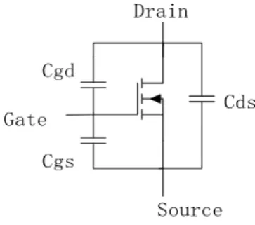
With the development of the full-controlled semiconductor devices, Power MOSFET (Metal Oxide Semiconductor Field Effect Transistor) has been applied widely in Switch Power Supply Technology, for whose characteristics of fast switching speed, good performance in high-frequency, low driver energy loss and easy to parallel. Power MOSFET is nearly an ideal switch, which has a high gain and fast switching speed. However, the parasitic capacitances existing in the Power MOSFET degrade performance of switch [1] [2]. Gate Drain Source Cds Cgd Cgs
Fig. 1 Equivalent circuit showing parasitic capacitance: the capacitance between the Gate and Source Cgs, the capacitance between the Gate and
Drain Cgd, the capacitance between Drain and Source Cds.
The switch process of Power MOSFET is the charge-discharge of the parasitic capacitances shown in Fig. 1. In order to decrease the influence of these parasitic capacitances, the gate driver circuit should meet the follow demands [3].
1. Trigger Pulse should rise and fall fast enough to decrease switching loss.
2. To reduce the Drain-to-Source drop voltage Vds when on state, sufficiently high gate-to-source voltage Vgs need to be supplied to guarantee Power MOSFET deeply saturated.
3. To ensure reliable turning off when off state, negative voltage should be provided to avoid unexpected turning on caused by electromagnetic interference.
4. Sufficient power should be able to provide to meet the required turn on energy.
Consideration of safety in most cases, the gate driver controller should be isolated to Power MOSFET. Therefore, pulse transformer is often used as an isolator that transfers driving signal and energy without auxiliary power source [4] [5] [6]. This paper designs a new gate driver circuit also using pulse transformer.
2. Gate Driver Circuits Using Pulse
Transformer
2.1 Conventional Driver
GND PWM Controller R1 C Rg VD TFig. 2 Conventional driver circuit
Fig. 2 shows the conventional driver circuit [3]. The blocking capacitor C is placed in series with the primary
winds of the pulse transformer to provide the reset voltage for the magnetizing inductance. Without the capacitor there would be a duty ratio dependent DC voltage across the winding and the transformer would saturate. However, the blocking capacitor C and the magnetizing inductance will excite the L-C resonance. In most cases this L-C resonance can be damped by primary resistor R1. Bidirectional Zener diode VD is used to decrease the
overshoot of the gate voltage Vgs. The gate resistor Rg is used to avoid the gate transient surge current. This kind of gate driver has advantages of simple structure, easy to be integrated while the amplitude of its output voltage reduces with the duty ratio increase. So the conventional driver is not suitable for working in large duty ratio.
2.2 Modified Driver
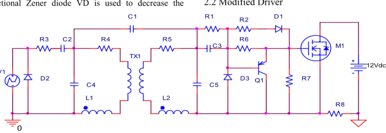
V1 0 R3 C3 C2 TX1 R7 12Vdc R8 Q1 R5 R6 R2 R4 R1 L1 L2 C4 C5 M1 C1 D3 D2 D1Fig. 3 Modified Driver Circuit A modified transformer-isolated gate driver circuit
simulation model is shown in Fig.3. The pulse transformer model consists of ideal transformer TX1, primary winding resistor R4, secondary winding resistor R5, transformer leakage inductance L1, L2, and distributed capacitance C1, C4, C5. Here, a bootstrap capacitor C3 and a bootstrap diode clamp D3 are used to restore the original gate drive amplitude on the secondary side of the transformer. When PWM signal turns low, the PNP transistor Q1 is used to accelerate the discharge of Cgs, and resistor R6 is not only used to maintain the base-to-emitter voltage of Q1 that
ensures Q1 to be on state, but also provides a discharge channel that will make collector-to-emitter voltage of Q1 down to zero. Secondary resistor R1 with bootstrap capacitor C3 and bootstrap diode D3 together constitute RCD absorbing circuit, which can suppress the resonance caused by leakage inductance. This driver provides a certain negative voltage to improve reliability of the off state reduces off-time and switch energy loss and has a good performance on widely range of duty ratio. However, it hardly reduces the rise-time and is sensitive to leakage inductance. So this kind of driver needs to be improved [3].
2.3 New Driver
12Vdc R8 C4 D3 V1 Q1 Q2 M1 C7 R5 C3 0 R2 C2 TX1 R4 R3 L1 L2 C5 C6 C1 R7 D1 D4 D2 D5 R1 R6This paper proposes a new gate driver circuit using pulse transformer that can provide negative voltage for off state, store energy to accelerate turning on. Fig. 4 shows the simulation model of the new driver. Here, pulse transformer model consists of ideal transformer TX1, primary and secondary winding resistor R3, R4, leakage inductance L1, L2, distributed capacitor C1, C5, C6. Compared to the modified driver, the new driver is added a series of components, includes energy storage capacitor C7, C4, totem pole constituted by NPN transistor Q1 and PNP transistor Q2, Zener diode D3 and simply diode D1. When PWM signal rises, C7 charges C4 and the gate firstly. With the process of gate charging, the voltage of C7 is gradually decreasing while the voltage of bootstrap diode D4 is increasing. After the two voltages equal, C7, C4 and Cgs all began to be charged by the voltage of bootstrap diode D4 until close of PWM signal rising. When PWM signal falls, Q1 turns off but Q2 turns on. Then, C4, which is charged from the C7 and transformer when PWM is high, supplies the negative voltage to gate-source capacitor Cgs through Q2. Zener diode D3 and simple diode D5 are used to control the voltage of C4. It can realize different negative voltage by changing the parameter of Zener diode D3.
3. Parameters Analysis
3.1 Pulse Transformer
Pulse transformer would be saturation if the current across it continues in a long duration [7] [8] [9]. In order to avoid saturation, the magnetizing inductance of the pulse transformer must be increased to decrease the magnetizing current. Therefore, the size of pulse transformer will be large. However, too large size goes against circuit integration. It is an optimization that alternates the cycle time and transformer size. In this paper, a new pulse transformer with one primary winding and two secondary winding was designed. The primary and secondary windings of it all had same numbers of turns.
3.2 Secondary side capacitors
Secondary side capacitors include bootstrap capacitor C3, energy storage capacitor C7, C4.
C4 is charged when PWM is high, ideal charged voltage
4 3
C D F EC
V
=
V
+ +
V V
. Where, VD3 is the voltage of D3, VF is the forward drop voltage of D5, and VEC is the emitter-to-collector voltage of Q2.When PWM signal turns to low, C4 charges the Cgs reversely.That is,
C V V
4*(
C4−
C4')
=
Q C
g+
iss*( '
V
C4− −
V V
F EC)
Where,
V
C4'
is the negative voltage of C4, Qg is the gate charge total, Ciss is the equalization input capacitor of Power MOSFET. In according to these analyses, the value of C4 and D3 can be calculated. Limited to the charge time, C4 hardly charge enough when PWM signal duty ratio is small. So it only can provide a low level negative voltage as shown in Fig. 10.C7 is used to supply the gate charge when PWM signal rises, and to be charged when PWM is on state. So the voltage of C7 varies in a cycle, which will impact on the transient response of the new driver circuit. Therefore, the value of C7 is always 5%~10% of C3.
Too large value of C3 will cause that the driver circuit can’t restore the amplitude of original PWM signal. But too small value of C3 will cause Vgs decreasing, which leads poor immunity. Generally, the value of C3 should be larger than the sum value of C7 and C4.
3.3 Blocking capacitor
The value of the blocking capacitor C2 directly determines ripple and amplitude of the drive current across it. The current needed to turn on Power MOSFET is,
3 drv g C
I
=
I
+
I
That is, 2 3 2 2 3 2 2 1 1 2(1
)
4(
)
g C C C T CQ
UD
D
U
C
C
U
U
L
L f
U
∆
−
=
+
+
∆
∆
+
∆
(1)The value of C2 is not only limited to Eq. (1), but also limited to transient response of the driver circuit. Therefore, the accuracy value of C2 needs to be more or less adjusted.
3.4 Matched load resistance
The matched load resistance includes primary resistor R2 and secondary resistor R3. In the primary circuit, primary resistor R2, primary winding resistor R3, PWM controller output resistor Rdrv, primary magnetizing inductance LT1, leakage inductance L1 and blocking capacitor C2 together form a RLC 2-order oscillation circuit [3].
Damping coefficient, 2 3 2 1 1
(
)
2
drv(
T)
R R R
C
L
L
ξ
=
+
+
+
Too small value of
ξ
will cause Vgs overshoot, but too large value ofξ
, that means R2 in a large value, willcause too large partial voltage of R2. Generally,
ξ
is slight less than 1.That is, 1 1 2 3 2
(
)
2
T drvL
L
R
R
R
C
+
<
−
−
.Secondary resistor R1, secondary winding resistor R4, secondary inductance LT2, secondary leakage inductance L2, bootstrap capacitor C3, and bootstrap D4 together constitute another RLC 2-order oscillation circuit in secondary side. When PWM controller happens to power interruption, the energy stored in the secondary winding will continue to charge C3 until the negative voltage of secondary winding is down to 0. It maybe leads Power MOSFET unexpected turning on. Secondary resistor R1 is used to decrease the voltage of C3 by providing a discharge channel. Generally, its value is 1k ohm.
3.5 Gate resistor
Gate resistor R5 is used to avoid surge charge current, which requires the value of R5 large enough. But too large value will decrease the turn on time of Power MOSFET. Fig. 5 shows the gate charge current curves in different gate resistor conditions. [10] [11].
It can be concluded in Fig. 5 that the charge time, which means the turn on time of Power MOSFET, increases with the increase of R5. However, the area enclosed by the charge current and charge time is constant because of constant Power MOSFET gate charge Qg.
-0.10 0 0.1 0.2 0.3 0.4 0.2 0.4 0.6 0.8 1 1.2 1.4 Time / us Ig / A f=100kHz, Id=5A, Vds=12V R5=1Ω R5=10Ω R5=5Ω
Fig. 5 Gate charge current curves
4. Simulation results
In order to verify the performance of the two driver circuit, this chapter use PSPICE software to carry out a simulation. The follows are the simulation results.
4.1 Steady-state response
Duty Ratio=0.1, f=100kHz, Iload=5A,Dload=12V PWM 5 6 7 8 9 10 11 12 13 14 15 -5 0 5 10 15 Time / us V gs
/ V New Driver Modified Driver
(a)
Duty Ratio=0.9, f=100kHz, Iload=5A, Vload=12V
0 1 2 3 4 5 6 7 8 9 -5 0 5 10 15 Time / us Vgs / V PWM Modified Driver New Driver (b)
Fig. 6 Steady-state response in different duty ratio conditions, (a) Small duty ratio, (b) Large duty ratio. Vgs: gate-to-source voltage; PWM signal
high level: 15V in new driver 12V in modified driver.
As shown in Fig. 6, the two drivers all have a good performance in the widely range of duty ratio though the amplitude of Vgs has a certain degree of attenuation in large duty ratio condition. Primary magnetizing current increases with the increase of duty ratio. Then the partial voltage of R2 increases, which will lead transform voltage decrease. So Vgs is attenuated. It’s also shown in Fig. 8 that the new driver can provide negative voltage to off state, but the amplitude of the negative voltage varies with the duty ratio. The amplitude voltage of new driver is less than the modified driver. And the difference will be remarkable in large duty ratio.
4.2 Anti-interference
Duty Ratio=0.5, f=100kHz, Iload=5A, Vload=12V, Ls=7uH
8 10 12 14 16 18 0 10 20 Time / us V gs / V PWM Modified Driver New Driver
Fig. 7 Steady-state response using a large leakage inductance transformer Fig. 6 shows the steady-state response when just the transformer nominal leakage inductance is considered. Fig. 7 shows the steady-state response when PCB tracing inductance is taken into account or a large leakage inductance transformer is used. As shown in the two figures, the new driver has a better performance on anti-interference. Bootstrap diode D4 and totem pole work together to isolate the impact of leakage inductance to Power MOSFET. D4 supplies a discharge channel to leakage inductance of transformer while totem pole supplies a charge-discharge channel to Cgs. The two channels are isolated to each other. Therefore, the oscillation generated by the leakage inductance of transformer can’t transfer to the gate of Power MOSFET.
4.3 Switching transient
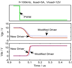
f=100kHz, Iload=5A, Vload=12V -5 0 5 10 15 Vgs / V -0.1 0 0.1 0.2 0.3 0.4 -5 0 5 10 15 Time / us Vds / V PWM Modified Driver New Driver Modified Driver New Driver Fig. 8 Trun on processf=100kHz, Iload=5A, Vload=12V -5 0 5 10 15 Vgs / V 4.9 5 5.1 5.2 5.3 5.4 5.5 -5 0 5 10 15 Time / us Vds / V PWM Modified Driver Modified Driver New Driver New Driver
Fig. 9 Turn off process
Fig. 8 shows the gate driver voltage Vgs curve and drain-to-source voltage Vds curve when PWM signal turns on. The modified driver energy is only supplied by bootstrap capacitor C3 and secondary winding. In addition to C3 and secondary winding, the new driver energy is also supplied by C7. So, the new driver has a larger gate charging current, which indicates steeper rising edge and shorter delay and turn on time. Fig. 9 shows the gate driver voltage Vgs curve and drain-to-source voltage Vds curve when PWM signal turns off. Due to the negative voltage supplied by C4, the new driver has slight larger discharge current and shorter discharge response delay time than the modified driver that although it also has Q1 to provide a rapid discharge channel. Overall, the new driver has a more excellent performance in response speed and turn on time.
4.4 Efficiency analysis
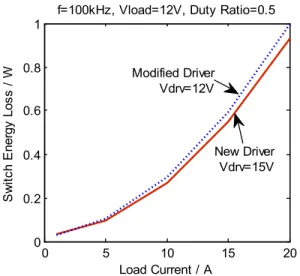
The energy loss is another import factor to evaluate the performance of driver circuit. This paper uses a concept of average power, i.e. the ratio of energy loss in a cycle and the cycle period [12].The switch energy loss can be calculated by Eq. (2). ( ) ( ) ( ) ( ) 0 ( ) ( ) 0
*
*
sw on sw off t M d s on d on t d s off d offP
V
I
dt f
V
I
dt f
=
∗
+
∗
∫
∫
(2)0 5 10 15 20 0 0.2 0.4 0.6 0.8 1 Load Current / A S w itc h E ner gy Los s / W
f=100kHz, Vload=12V, Duty Ratio=0.5
Modified Driver Vdrv=12V
New Driver Vdrv=15V
Fig. 10 Switch energy loss
Fig. 10 shows the switch energy curves of the two drivers in different drain (load) current. The switch energy loss of the two drivers all increase with the increase of current. However, the new driver switch energy is smaller due to its faster switch speed.
5. Conclusions
There are many kinds of power MOSFET Gate driver circuit current, and each of those has its merit and demerit and applicable situation. In this paper, two kinds topologies is introduced, one is the modified driver circuit using pulse transformer, and another one is new diver circuit. The results of simulation prove that the modified driver has stable driving voltage, a wide duty ratio control range, but its performance is sensitive to leakage and PCB trace inductance. However, the new driver has a faster switch speed, shorter switch delay time and lower switch energy loss. Furthermore, the new driver has a better reliability because it can supply negative voltage to off state, and has good anti-interference to leakage inductance. Overall, the new driver has a good significance in application.
References
[1] K.S.Oh, "MOSFET Basics", FAIRCHILD, Dev. 4, July 2000. [2] Ray Ridley, "Gate Drive Design Tips", Power Systems
Design Europe, December 2006, pp. 14-18.
[3] Laszlo Balogh, "Design and Application Guide for High Speed MOSFET Gate Drive Circuits", International Rectifier, Technical Paper.
[4] Zhiliang Zhang, Wilson Eberle and Yan-Fei Liu, "A 1-MHz High-Efficiency 12-V Buck Voltage Regulator with a New Current-Source Gate Driver", IEEE TRANSACTIONS ON POWER ELECTRONICS, Vol. 23, No. 6, November 2008, pp. 2817-2827.
[5] L. Bolduc, A. Gaudreau and A. Dutil, "Saturation time of transformers under dc excitation", Electric Power Systems Research 56 (2000) 95–102.
[6] D. Bortis, G. Ortiz, J.W. Kolar and J. Biela, "Design Procedure for Compact Pulse Transformers with Rectangular Pulse Shape and Fast Rise Times", IEEE Transactions on Dielectrics and Electrical Insulation, Vol. 18, No. 4; August 2011, pp. 1171-1180.
[7] Patrick Scoggins, "A Guide to Designing Gate-Drive Transformers", Power Electronics Technology, January 2007, pp. 32-36.
[8] Jean-Christophe Crébier and Nicolas Rouger, "Loss Free Gate Driver Unipolar Power Supply for High Side Power Transistors", IEEE TRANSACTIONS ON POWER ELECTRONICS, Vol. 23, No. 3, May 2008, pp. 1565-1573. [9] J.Cˇ. Mikulovic´, · M.S. Savic, "Calculation of transients in
transformer winding and determination of winding parameters", Electr Eng (2007) 89: 293–300.
[10] Zhiliang Zhang, Wilson Eberle, Zhihua Yang, Yan-Fei Liu and Paresh C. Sen, "Optimal Design of Resonant Gate Driver for Buck Converter Based on a New Analytical Loss Model", IEEE TRANSACTIONS ON POWER ELECTRONICS, Vol. 23, No. 2, March 2008, pp. 653-666.
Daizhuang Wang received the B.E. degree from the school of Automotive Engineering, Harbin Institute of Technology, Weihai, China, in 2011. Currently, he is a postgraduate in Clean Energy Automotive Engineering Center, Tongji University, Shanghai, China. His current interests include lithium-ion battery management system, lithium-ion battery pack equalization system, DC-DC Converter, and Power MOSFET driver circuit.
Haifeng Dai received his B.E. degree from the School of Mechanical Engineeing, Tongji University, Shanghai, China, in 2003. He was received the Ph. D from Tongji University, Shanghai, China, in 2008. He is currently a lecturer in Clean Energy Automotive Engineering Center, Tongji University, Shanghai, China. His current research interests include storage battery management system, wireless charging technology and DC-DC converter.
Zechang Sun received his B.E. and M.E. degree from the Department of Motor, Harbin Institute of Technology, Harbin, China, in 1976 and 1981, respectively. From 1986 to 1987, he was a Visiting Scholar in TH Darmstadt of Germany, where he was engaged in research on Power Electronics and DC-DC Converter. He was received the Ph. D in “Pattern Recognition and Intelligent Control” from Tongji University, Shanghai, China, in 1988. He is currently a Professor in Clean Energy Automotive Engineering Center, Tongji University, Shanghai, China. His current research interests include clean energy automotive power train system integration and control, electro-hydraulic braking system, and Storage battery management system.
![Fig. 5 shows the gate charge current curves in different gate resistor conditions. [10] [11]](https://thumb-us.123doks.com/thumbv2/123dok_us/9467536.2428074/4.918.495.776.129.660/fig-shows-charge-current-curves-different-resistor-conditions.webp)