42
C H A P T E R
10
T I M I N G I S S U E S
I N D I G I T A L C I R C U I T S
nImpact of clock skew and jitter on performance and functionality
n
Alternative timing methodologies
n
Synchronization issues in digital IC and board design
Clock generation
10.1 Introduction
10.2 Classification of Digital Systems 10.3 Synchronous Design — An In-depth
Perspective
10.3.1Synchronous Timing Basics 10.3.2Sources of Skew and Jitter 10.3.3Clock-Distribution Techniques 10.3.4Latch-Based Clocking 10.4 Self-Timed Circuit Design*
10.5 Synchronizers and Arbiters*
10.6 Clock Synthesis and Synchronization Using a Phase-Locked Loop
10.7 Future Directions
10.8 Perspective: Synchronous versus Asynchronous Design
10.9 Summary 10.10 To Probe Further
10.1 Introduction
All sequential circuits have one property in common—a well-defined ordering of the switching events must be imposed if the circuit is to operate correctly. If this were not the case, wrong data might be written into the memory elements, resulting in a functional fail-ure. The synchronous system approach, in which all memory elements in the system are simultaneously updated using a globally distributed periodic synchronization signal (that is, a global clock signal), represents an effective and popular way to enforce this ordering. Functionality is ensured by imposing some strict contraints on the generation of the clock signals and their distribution to the memory elements distributed over the chip; non-com-pliance often leads to malfunction.
This Chapter starts with an overview of the different timing methodologies. The majority of the text is devoted to the popular synchronous approach. We analyze the impact of spatial variations of the clock signal, called clock skew, and temporal variations of the clock signal, called clock jitter, and introduce techniques to cope with it. These vari-ations fundamentally limit the performance that can be achieved using a conventional design methodology.
At the other end of the design spectrum is an approach called asynchronous design, which avoids the problem of clock uncertainty all-together by eliminating the need for globally-distributed clocks. After discussing the basics of asynchronous design approach, we analyze the associated overhead and identify some practical applications. The impor-tant issue of synchronization, which is required when interfacing different clock domains or when sampling an asynchronous signal, also deserves some in-depth treatment. Finally, the fundamentals of on-chip clock generation using feedback is introduced along with trends in timing.
10.2 Classification of Digital Systems
In digital systems, signals can be classified depending on how they are related to a local clock [Messerschmitt90][Dally98]. Signals that transition only at predetermined periods in time can be classified as synchronous, mesochronous, or plesiochronous with respect to a system clock. A signal that can transition at arbitrary times is considered asynchronous.
10.2.1 Synchronous Interconnect
A synchronous signal is one that has the exact same frequency, and a known fixed phase offset with respect to the local clock. In such a timing methodology, the signal is “synchro-nized” with the clock, and the data can be sampled directly without any uncertainty. In digital logic design, synchronous systems are the most straightforward type of intercon-nect, where the flow of data in a circuit proceeds in lockstep with the system clock as shown below.
Here, the input data signal In is sampled with register R1to give signal Cin, which is synchronous with the system clock and then passed along to the combinational logic block. After a suitable setting period, the output Coutbecomes valid and can be sampled by
R2which synchronizes the output with the clock. In a sense, the “certainty period” of sig-nal Cout, or the period where data is valid is synchronized with the system clock, which allows register R2to sample the data with complete confidence. The length of the “uncer-tainty period,” or the period where data is not valid, places an upper bound on how fast a synchronous interconnect system can be clocked.
10.2.2 Mesochronous interconnect
A mesochronous signal is one that has the same frequency but an unknown phase offset with respect to the local clock (“meso” from Greek is middle). For example, if data is being passed between two different clock domains, then the data signal transmitted from the first module can have an unknown phase relationship to the clock of the receiving module. In such a system, it is not possible to directly sample the output at the receiving module because of the uncertainty in the phase offset. A (mesochronous) synchronizer can be used to synchronize the data signal with the receiving clock as shown below. The syn-chronizer serves to adjust the phase of the received signal to ensure proper sampling.
In Figure 10.2, signal D1is synchronous with respect to ClkA. However, D1and D2
are mesochronous with ClkBbecause of the unknown phase difference between ClkAand
ClkBand the unknown interconnect delay in the path between Block A and Block B. The
role of the synchronizer is to adjust the variable delay line such that the data signal D3(a
delayed version of D2) is aligned properly with the system clock of block B. In this exam-ple, the variable delay element is adjusted by measuring the phase difference between the received signal and the local clock. After register R2samples the incoming data during the
certainty period, then signal D4becomes synchronous with ClkB.
10.2.3 Plesiochronous Interconnect
A plesiochronous signal is one that has nominally the same, but slightly different fre-quency as the local clock (“plesio” from Greek is near). In effect, the phase difference
R1 Combinational R2 CLK Out Cout In Cin
Figure 10.1 Synchronous interconnect methodology. Logic R1 Interconnect R2 ClkA D2 Block A Delay Block B ClkB D4 PD/ Control D1
Figure 10.2 Mesochronous communication approach using variable delay line.
drifts in time. This scenario can easily arise when two interacting modules have indepen-dent clocks generated from separate crystal oscillators. Since the transmitted signal can arrive at the receiving module at a different rate than the local clock, one needs to utilize a buffering scheme to ensure all data is received. Typically, plesiochronous interconnect only occurs in distributed systems like long distance communications, since chip or even board level circuits typically utilize a common oscillator to derive local clocks. A possible framework for plesiochronous interconnect is shown in Figure 10.3.
In this digital communications framework, the originating module issues data at some unknown rate characterized by C1, which is plesiochronous with respect to C2. The timing recovery unit is responsible for deriving clock C3from the data sequence, and buff-ering the data in a FIFO. As a result, C3will be synchronous with the data at the input of the FIFO and will be mesochronous with C1. Since the clock frequencies from the origi-nating and receiving modules are mismatched, data might have to be dropped if the trans-mit frequency is faster, and data can be duplicated if the transtrans-mit frequency is slower than the receive frequency. However, by making the FIFO large enough, and periodically reset-ting the system whenever an overflow condition occurs, robust communication can be achieved.
10.2.4 Asynchronous Interconnect
Asynchronous signals can transition at any arbitrary time, and are not slaved to any local clock. As a result, it is not straightforward to map these arbitrary transitions into a syn-chronized data stream. Although it is possible to synchronize asynchronous signals by detecting events and introducing latencies into a data stream synchronized to a local clock, a more natural way to handle asynchronous signals is to simply eliminate the use of local clocks and utilize a self-timed asynchronous design approach. In such an approach, com-munication between modules is controlled through a handshaking protocol to perform the proper ordering of commands.
Originating Receiving FIFO Timing Clock C1 Clock C2 Module Module Recovery C3
Figure 10.3 Plesiochronous communications using FIFO.
Figure 10.4 Asynchronous design methodology for simple pipeline interconnect.
Reg Self-TimedLogic
Interconnect Circuit
Reg Self-TimedLogic
Interconnect Circuit Req Ack handshaking signals Data I DV I DV
When a logic block completes an operation, it will generate a completion signal DV to indicate that output data is valid. The handshaking signals then initiate a data transfer to the next block, which latches in the new data and begins a new computation by asserting the initialization signal I. Asynchronous designs are advantageous because computations are performed at the native speed of the logic, where block computations occur whenever data becomes available. There is no need to manage clock skew, and the design methodol-ogy leads to a very modular approach where interaction between blocks simply occur through a handshaking procedure. However, these handshaking protocols result in increased complexity and overhead in communication that can reduce performance.
10.3 Synchronous Design — An In-depth Perspective
10.3.1 Synchronous Timing Basics
Virtually all systems designed today use a periodic synchronization signal or clock. The generation and distribution of a clock has a significant impact on performance and power dissipation. For a positive edge-triggered system, the rising edge of the clock is used to denote the beginning and completion of a clock cycle. In the ideal world, assuming the clock paths from a central distribution point to each register are perfectly balanced, the phase of the clock (i.e., the position of the clock edge relative to a reference) at various points in the system is going to be exactly equal. However, the clock is neither perfectly periodic nor perfectly simultaneous. This results in performance degradation and/or circuit malfunction. Figure 10.5 shows the basic structure of a synchronous pipelined datapath. In
the ideal scenario, the clock at registers 1 and 2 have the same clock period and transition at the exact same time. The following timing parameters characterize the timing of the sequential circuit.
• The contamination (minimum) delay tc-q,cd, and maximum propagation delay of the register tc-q.
• The set-up (tsu) and hold time (thold) for the registers.
• The contamination delay tlogic,cd and maximum delay tlogicof the combinational logic. CLK Q D In Combinational Logic D Q
Figure 10.5 Pipelined Datapath Circuit and timing parameters. tc-q tc-q, cd tlogic tlogic, cd tsu,thold tCLK1 tCLK2 R1 R2
• tclk1and tclk2, corresponding to the position of the rising edge of the clock relative to a global reference.
Under ideal conditions (tclk1= tclk2), the worst case propagation delays determine the minimum clock period required for this sequential circuit. The period must be long enough for the data to propagate through the registers and logic and be set-up at the desti-nation register before the next rising edge of the clock. This constraint is given by (as derived in Chapter 7):
(10.1) At the same time, the hold time of the destination register must be shorter than the mini-mum propagation delay through the logic network,
(10.2) The above analysis is simplistic since the clock is never ideal. As a result of process and environmental variations, the clock signal can have spatial and temporal variations. Clock Skew
The spatial variation in arrival time of a clock transition on an integrated circuit is com-monly referred to as clock skew. The clock skew between two points i and j on a IC is given byδ(i,j) = ti- tj, where tiand tjare the position of the rising edge of the clock with respect to a reference. Consider the transfer of data between registers R1 and R2 in Figure 10.5. The clock skew can be positive or negative depending upon the routing direction and position of the clock source. The timing diagram for the case with positive skew is shown in Figure 10.6. As the figure illustrates, the rising clock edge is delayed by a positiveδat the second register.
Clock skew is caused by static path-length mismatches in the clock load and by def-inition skew is constant from cycle to cycle. That is, if in one cycle CLK2 lagged CLK1 by δ, then on the next cycle it will lag it by the same amount. It is important to note that clock skew does not result in clock period variation, but rather phase shift.
T>tc–q+tlogic+tsu
tho ld<tc–q c d, +tlogic cd,
CLK1
CLK2
TCLK
Figure 10.6 Timing diagram to study the impact of clock skew on performance and funcationality. In this sample timing diagram,δ> 0.
δ δ + th TCLK+ δ 1 2 3 4
Skew has strong implications on performance and functionality of a sequential sys-tem. First consider the impact of clock skew on performance. From Figure 10.6, a new input In sampled by R1 at edge1 will propagate through the combinational logic and be sampled by R2 on edge4. If the clock skew is positive, the time available for signal to propagate from R1 to R2 is increased by the skewδ. The output of the combinational logic must be valid one set-up time before the rising edge of CLK2 (point4). The constraint on the minimum clock period can then be derived as:
(10.3) The above equation suggests that clock skew actually has the potential to improve the performance of the circuit. That is, the minimum clock period required to operate the circuit reliably reduces with increasing clock skew! This is indeed correct, but unfortu-nately, increasing skew makes the circuit more susceptible to race conditions may and harm the correct operation of sequential systems.
As above, assume that input In is sampled on the rising edge of CLK1 at edge1 into R1. The new values at the output of R1 propagates through the combinational logic and should be valid before edge4 at CLK2. However, if the minimum delay of the combina-tional logic block is small, the inputs to R2 may change before the clock edge2, resulting in incorrect evaluation. To avoid races, we must ensure that the minimum propagation delay through the register and logic must be long enough such that the inputs to R2 are valid for a hold time after edge2. The constraint can be formally stated as
(10.4) Figure 10.7 shows the timing diagram for the case whenδ< 0. For this case, the ris-ing edge of CLK2 happens before the risris-ing edge of CLK1. On the risris-ing edge of CLK1, a new input is sampled by R1. The new sampled data propagates through the combinational logic and is sampled by R2 on the rising edge of CLK2, which corresponds to edge4. As can be seen from Figure 10.7 and Eq. (10.3), a negative skew directly impacts the perfor-mance of sequential system. However, a negative skew implies that the system never fails, since edge2 happens before edge 1! This can also be seen from Eq. (10.4), which is always satisfied sinceδ< 0.
T+δ≥tc–q+tlogic +ts u or T≥tc–q+tlogic+tsu–δ δ+thol d<t(c–q,cd)+t(logic,cd) δ<t(c–q,cd)+t(logic,cd)–thold or CLK1 CLK2 TCLK δ TCLK+ δ
Figure 10.7 Timing diagram for the case whenδ< 0. The rising edge of CLK2 arrives earlier than the edge of CLK1.
1 2
3 4
Example scenarios for positive and negative clock skew are shown in Figure 10.8.
• δ > 0—This corresponds to a clock routed in the same direction as the flow of the data through the pipeline (Figure 10.8a). In this case, the skew has to be strictly controlled and satisfy Eq. (10.4). If this constraint is not met, the circuit does malfunction indepen-dent of the clock period. Reducing the clock frequency of an edge-triggered circuit does not help get around skew problems! On the other hand, positive skew increases the throughput of the circuit as expressed by Eq. (10.3), because the clock period can be shortened byδ. The extent of this improvement is limited as large values ofδsoon pro-voke violations of Eq. (10.4).
• δ< 0—When the clock is routed in the opposite direction of the data (Figure 10.8b), the skew is negative and condition (10.4) is unconditionally met. The circuit operates cor-rectly independent of the skew. The skew reduces the time available for actual computa-tion so that the clock period has to be increased by|δ|. In summary, routing the clock in the opposite direction of the data avoids disasters but hampers the circuit performance . Unfortunately, since a general logic circuit can have data flowing in both directions (for example, circuits with feedback), this solution to eliminate races will not always work (Figure 10.9). The skew can assume both positive and negative values depending on the direction of
(a) Positive skew
Figure 10.8 Positive and negative clock skew. (b) Negative skew CLK Q D In Combinational Logic D Q D Q Combinational Logic tCLK1 tCLK2 tCLK3 R1 R2 R3 delay delay CLK Q D In Combinational Logic D Q D Q Combinational Logic tCLK1 tCLK2 tCLK3 R1 R2 R3 delay delay
Figure 10.9 Datapath structure with feedback.
RE G REG CLK RE G RE G Out In Clock distribution Positive skew Negative skew Logic CLK Logic CLK CLK Logic
the data transfer. Under these circumstances, the designer has to account for the worst-case skew condition. In general, routing the clock so that only negative skew occurs is not feasible. Therefore, the design of a low-skew clock network is essential.
Example 10.1 Propagation and Contamination Delay Estimation
Consider the logic network shown in Figure 10.10. Determine the propagation and contami-nation delay of the network, assuming that the worst case gate delay is tgate. The maximum
and minimum delays of the gates is made, as they are assumed to be identical.
The contamination delay is given by 2 tgate(the delay through OR1and OR2). On the
other hand, computation of the worst case propagation delay is not as simple as it appears. At first glance, it would appear that the worst case corresponds to path1and the delay is 5tgate.
However, when analyzing the data dependencies, it becomes obvious that path1is never exercised. Path1is called a false path. If A = 1, the critical path goes through OR1and OR2.
If A = 0 and B = 0, the critical path is through I1,OR1and OR2(corresponding to a delay of 3
tgate). For the case when A= 0 and B =1, the critical path is through I1,OR1, AND3and OR2. In
other words, for this simple (but contrived) logic circuit, the output does not even depend on inputs C and D (that is, there is redundancy). Therefore, the propagation delay is 4 tgate. Given
the propagation and contamination delay, the minimum and maximum allowable skew can be easily computed.
WARNING: The computation of the worst-case propagation delay for combinational logic, due to the existence of false paths, cannot be obtained by simply adding the propa-gation delay of individual logic gates. The critical path is strongly dependent on circuit topology and data dependencies.
Clock Jitter
Clock jitter refers to the temporal variation of the clock period at a given point — that is, the clock period can reduce or expand on a cycle-by-cycle basis. It is strictly a temporal uncertainty measure and is often specified at a given point on the chip. Jitter can be mea-sured and cited in one of many ways. Cycle-to-cycle jitter refers to time varying deviation
C
D A
Figure 10.10 Logic network for computation of performance. AND1 AND2 AND3 OR1 OR2 path1 B I1 path2
of a single clock period and for a given spatial location i is given as Tjitter,i(n) = Ti,n+1- Ti,n - TCLK, where Ti,nis the clock period for period n, Ti,n+1is clock period for period n+1, and TCLKis the nominal clock period.
Jitter directly impacts the performance of a sequential system. Figure 10.11 shows the nominal clock period as well as variation in period. Ideally the clock period starts at edge2and ends at edge 5 and with a nominal clock period of TCLK. However, as a result of jitter, the worst case scenario happens when the leading edge of the current clock period is delayed (edge3), and the leading edge of the next clock period occurs early (edge 4). As a result, the total time available to complete the operation is reduced by 2 tjiiterin the worst case and is given by
(10.5) The above equation illustrates that jitter directly reduces the performance of a sequential circuit. Care must be taken to reduce jitter in the clock network to maximize performance.
Impact of Skew and Jitter on Performance
In this section, the combined impact of skew and jitter is studied with respect to conven-tional edge-triggered clocking. Consider the sequential circuit show in Figure 10.12.
Assume that nominally ideal clocks are distributed to both registers (the clock period is identical every cycle and the skew is 0). In reality, there is static skewδbetween the two clock signals (assume thatδ > 0). Assume that CLK1 has a jitter of tjitter1 and CLK2 has a jitter of tjitter2. To determine the constraint on the minimum clock period, we must look at the minimum available time to perform the required computation. The worst case happen when the leading edge of the current clock period on CLK1 happens late (edge3) and the leading edge of the next cycle of CLK2 happens early (edge ). This results in the following constraint
(10.6) TCL K–2tj itt er≥tc–q+tlogi c +ts u or T≥tc–q+tlogic+ts u+2tj itt er
Figure 10.11 Circuit for studying the impact of jitter on performance. CLK -tjitter TCLK tjitter CLK In Combinational Logic tc-q, tc-q, cd tlogic tlogic, cd tsu,thold REGS tjitter 1 2 3 4 5 6
TC LK+δ–tj itt er1–tjit ter 2≥tc–q+tlogi c +tsu T≥tc–q+tlogic+tsu–δ+tjit ter 1+tjit ter 2 or
As the above equation illustrates, while positive skew can provide potential perfor-mance advantage, jitter has a negative impact on the minimum clock period. To formulate the minimum delay constraint, consider the case when the leading edge of the CLK1 cycle arrives early (edge1) and the leading edge the current cycle of CLK2 arrives late (edge 6). The separation between edge 1 and 6 should be smaller than the minimum delay through the network. This results in
(10.7) The above relation indicates that the acceptable skew is reduced by the jitter of the two signals.
Now consider the case when the skew is negative (δ<0) as shown in Figure 10.13. For the timing shown, |δ| > tjitter2. It can be easily verified that the worst case timing is exactly the same as the previous analysis, withδ taking a negative value. That is, negative skew reduces performance.
Q D In Combinational Logic D Q tCLK1 tCLK2 R1 R2
Figure 10.12 Sequential circuit to study the impact of skew and jitter on edge-triggered systems. In this example, a positive skew (δ) is assumed.
CLK1 CLK2 TCLK δ TCLK+ δ 11 tjitter2 12 tjitter1 5 2 3 1 6 4 7 8 9
δ+thold+tji tter 1+tji tte r 2<t(c–q,c d)+t(logi c,cd)
δ<t(c–q,cd)+t(logic,cd)–thold–tj itt er1–tjit ter 2 or
Figure 10.13 Consider a negative clock skew (δ) and the skew is assumed to be larger than the jitter. CLK1 CLK2 TCLK δ < 0 TCLK+δ tjitter2 tjitter1 2 1 3 6 4 5 11 12 7 8 9
10.3.2 Sources of Skew and Jitter
A perfect clock is defined as perfectly periodic signal that is simultaneous triggered at var-ious memory elements on the chip. However, due to a variety of process and environmen-tal variations, clocks are not ideal. To illustrate the sources of skew and jitter, consider the simplistic view of clock generation and distribution as shown in Figure 10.14. Typically, a high frequency clock is either provided from off chip or generated on-chip. From a central point, the clock is distributed using multiple matched paths to low-level memory ele-ment.s registers. In this picture, two paths are shown. The clock paths include wiring and the associated distributed buffers required to drive interconnects and loads. A key point to realize in clock distribution is that the absolute delay through a clock distribution path is not important; what matters is the relative arrival time between the output of each path at the register points (i.e., it is pefectly acceptable for the clock signal to take multiple cycles to get from a central distribution point to a low-level register as long as all clocks arrive at the same time to different registers on the chip).
The are many reasons why the two parallel paths don’t result in exactly the same delay. The sources of clock uncertainty can be classified in several ways. First, errors can be divided into systematic or random. Systematic errors are nominally identical from chip to chip, and are typically predictable (e.g., variation in total load capacitance of each clock path). In principle, such errors can be modeled and corrected at design time given suffi-ciently good models and simulators. Failing that, systematic errors can be deduced from measurements over a set of chips, and the design adjusted to compensate. Random errors are due to manufacturing variations (e.g., dopant fluctuations that result in threshold vari-ations) that are difficult to model and eliminate. Mismatch may also be characterized as static or time-varying. In practice, there is a continuum between changes that are slower than the time constant of interest, and those that are faster. For example, temperature vari-ations on a chip vary on a millisecond time scale. A clock network tuned by a one-time calibration or trimming would be vulnerable to time-varying mismatch due to varying thermal gradients. On the other hand, to a feedback network with a bandwidth of several megahertz, thermal changes appear essentially static. For example, the clock net is usually by far the largest single net on the chip, and simultaneous transitions on the clock drivers induces noise on the power supply. However, this high speed effect does not contribute to
Figure 10.14 Skew and jitter sources in synchronous clock distribution. Clock Generation Devices Power Supply Interconnect Capacitive Load Temperature
Coupling to Adjacent Lines
7 1 2 3 4 5 6
time-varying mismatch because it is the same on every clock cycle, affecting each rising clock edge the same way. Of course, this power supply glitch may still cause static mis-match if it is not the same throughout the chip. Below, the various sources of skew and jit-ter, introduced in Figure 10.14, are described in detail.
Clock-Signal Generation (1)
The generation of the clock signal itself causes jitter. A typical on-chip clock generator, as described at the end of this chapter, takes a low-frequency reference clock signal, and pro-duces a high-frequency global reference for the processor. The core of such a generator is a Voltage-Controlled Oscillator (VCO). This is an analog circuit, sensitive to intrinsic device noise and power supply variations. A major problem is the coupling from the sur-rounding noisy digital circuitry through the substrate. This is particularly a problem in modern fabrication processes that combine a lightly-doped epitaxial layer and a heavily-doped substrate (to combat latch-up). This causes substrate noise to travel over large dis-tances on the chip. These noise source cause temporal variations of the clock signal that propagate unfiltered through the clock drivers to the flip-flops, and result in cycle-to-cycle clock-period variations. This jitter causes performance degradation.
Manufacturing Device Variations (2)
Distributed buffers are integral components of the clock distribution networks, as they are required to drive both the register loads as well as the global and local interconnects. The matching of devices in the buffers along multiple clock paths is critical to minimizing tim-ing uncertainty. Unfortunately, as a result of process variations, devices parameters in the buffers vary along different paths, resulting in static skew. There are many sources of vari-ations including oxide varivari-ations (that affects the gain and threshold), dopant varivari-ations, and lateral dimension (width and length) variations. The doping variations can affect the depth of junction and dopant profiles and cause variations in electrical parameters such as device threshold and parasitic capacitances. The orientation of polysilicon can also have a big impact on the device parameters. Keeping the orientation the same across the chip for the clock drivers is critical.
Variation in the polysilicon critical dimension, is particularly important as it trans-lates directly into MOS transistor channel length variation and resulting variations in the drive current and switching characteristics. Spatial variation usually consists of wafer-level (or within-wafer) variation and die-wafer-level (or within-die) variation. At least part of the variation is systematic and can be modeled and compensated for. The random variations however, ultimately limits the matching and skew that can be achieved.
Interconnect Variations (3)
Vertical and lateral dimension variations cause the interconnect capacitance and resistance to vary across a chip. Since this variation is static, it causes skew between different paths. One important source of interconnect variation is the Inter-level Dielectric (ILD) thickness variations. In the formation of aluminum interconnect, layers of silicon dioxide are inter-posed between layers of patterned metallization. The oxide layer is deposited over a layer of patterned metal features, generally resulting in some remaining step height or surface topography. Chemical-mechanical polishing (CMP) is used to “planarize” the surface and remove topography resulting from deposition and etch (as shown in Figure 10.15a). While at the feature scale (over an individual metal line), CMP can achieve excellent planarity, there are limitations on the planarization that can be achieved over a global range. This is primarily caused due to variations in polish rate that is a function of the circuit layout den-sity and pattern effects. Figure 10.15b shows this effect where the polish rate is higher for the lower spatial density region, resulting in smaller dielectric thickness and higher capac-itance.
The assessment and control of variation is of critical importance in semiconductor process development and manufacturing. Significant advances have been made to develop analytical models for estimating the ILD thickness variations based on spatial density. Since this component is often predictable from the layout, it is possible to actually correct for the systematic component at design time (e.g., by adding appropriate delays or making the density uniform by adding “dummy fills”). Figure 10.16 shows the spatial pattern den-sity and ILD thickness for a high performance microprocessor. The graphs show that there is clear correlation between the density and the thickness of the dielectric. So clock distri-bution networks must exploit such information to reduce clock skew.
Other interconnect variations include deviation in the width of the wires and line spacing. This results from photolithography and etch dependencies. At the lower levels of metallization, lithographic effects are important while at higher levels etch effects are important that depend on width and layout. The width is a critical parameter as it directly impacts the resistance of the line and the wire spacing affects the wire-to-wire
capaci-(b) Reality ρ1=low ρ2=high t=t1 t=t2 t=t3 Oxide Metal
Figure 10.15 Inter-level Dielectric (ILD) thickness variation due to density (coutersy of Duane Boning).
tance, which the dominant component of capacitance. A detailed review of device and interconnect variations is presented in [Boning00].
Environmental Variations (4 and 5)
Environmental variations are probably the most significant and primarily contribute to skew and jitter. The two major sources of environmental variations are temperature and power supply. Temperature gradients across the chip is a result of variations in power dis-sipation across the die. This has particularly become an issue with clock gating where some parts of the chip maybe idle while other parts of the chip might be fully active. This results in large temperature variations. Since the device parameters (such as threshold, mobility, etc.) depend strongly on temperature, buffer delay for a clock distribution net-work along one path can vary drastically for another path. More importantly, this compo-nent is time-varying since the temperature changes as the logic activity of the circuit varies. As a result, it is not sufficient to simulate the clock networks at worst case corners of temperature; instead, the worst-case variation in temperature must be simulated. An interesting question is does temperature variation contribute to skew or to jitter? Clearly the variation in temperature is time varying but the changes are relatively slow (typical time constants for temperature on the order of milliseconds). Therefore it usually consid-ered as a skew component and the worst-case conditions are used. Fortunately, using feed-back, it is possible to calibrate the temperature and compensate.
Power supply variations on the hand is the major source of jitter in clock distribu-tion networks. The delay through buffers is a very strong funcdistribu-tion of power supply as it directly affects the drive of the transistors. As with temperature, the power supply voltage is a strong function of the switching activity. Therefore, the buffer delay along one path is very different than the buffer delay along another path. Power supply variations can be classified into static (or slow) and high frequency variations. Static power supply varia-tions may result from fixed currents drawn from various modules, while high-frequency variations result from instantaneous IR drops along the power grid due to fluctuations in switching activity. Inductive issues on the power supply are also a major concern since they cause voltage fluctuations. This has particularly become a concern with clock gating as the load current can vary dramatically as the logic transitions back and forth between the idle and active states. Since the power supply can change rapidly, the period of the
Figure 10.16 Pattern density and ILD thickness variation for a high performance microprocessor. (a) Pattern Density (b) ILD thickness variation
clock signal is modulated on a cycle-by-cycle basis, resulting in jitter. The jitter on two different clock points maybe correlated or uncorrelated depending on how the power net-work is configured and the profile of switching patterns. Unfortunately, high-frequency power supply changes are difficult to compensate even with feedback techniques. As a result, power supply noise fundamentally limits the performance of clock networks. Capacitive Coupling (✖and✗)
The variation in capacitive load also contributes to timing uncertainty. There are two major sources of capacitive load variations: coupling between the clock lines and adjacent signal wires and variation in gate capacitance. The clock network includes both the inter-connect and the gate capacitance of latches and registers. Any coupling between the clock wire and adjacent signal results in timing uncertainty. Since the adjacent signal can transi-tion in arbitrary directransi-tions and at arbitrary times, the exactly coupling to the clock network is not fixed from cycle-to-cycle. This results in clock jitter. Another major source of clock uncertainty is variation in the gate capacitance related to the sequential elements. The load capacitance is highly non-linear and depends on the applied voltage. In many latches and registers this translates to the clock load being a function of the current state of the latch/register (this is, the values stored on the internal nodes of the circuit), as well as the next state. This causes the delay through the clock buffers to vary from cycle-to-cycle, causing jitter.
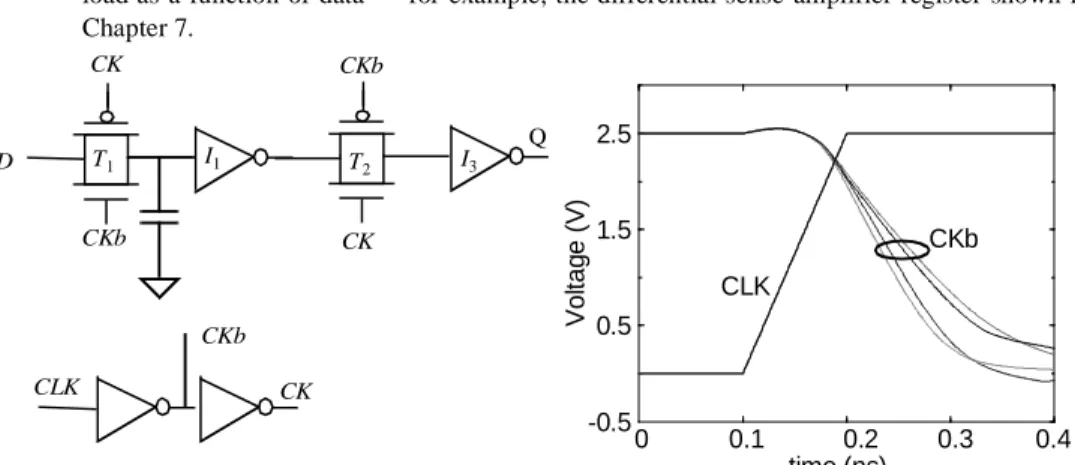
Example 10.2 Data-dependent Clock Jitter
Consider the circuit shown in Figure 10.17, where a minimum-sized local clock buffer drives a register (actually, four registers are driven, though only one is shown here). The simulation shows CKb, the output of the first inverter for four possible transitions (00, 01, 10 and 11). The jitter on the clock based on data-dependent capacitance is illustrated. In general, the only way to deal with this problem is to use registers that don’t exhibit a large variation in load as a function of data — for example, the differential sense-amplifier register shown in Chapter 7. D CK Q T1 I1 T2 I3 CKb CLK CKb CKb CK CK
Figure 10.17 Impact of data-dependent clock load on clock jitter for pass-transistor register.
-0.5 0.5 1.5 2.5 0 0.1 0.2 0.3 0.4 CLK CKb time (ns) Vol tag e (V )
10.3.3 Clock-Distribution Techniques
It is clear from the previous discussion that clock skew and jitter are major issues in digital circuits, and can fundamentally limit the performance of a digital system. It is necessary to design a clock network that minimizes skew and jitter. Another important consideration in clock distribution is the power dissipation. In most high-speed digital processors, a major-ity of the power is dissipated in the clock network. To reduce power dissipation, clock net-works must support clock conditioning — this is, the ability to shut down parts of the clock network. Unfortunately, clock gating results in additional clock uncertainty.
In this section, an overview of basic constructs in high-performance clock distribu-tion techniques is presented along with a case study of clock distribudistribu-tion in the Alpha microprocessor. There are many degrees of freedom in the design of a clock network including the type of material used for wires, the basic topology and hierarchy, the sizing of wires and buffers, the rise and fall times, and the partitioning of load capacitances. Fabrics for clocking
Clock networks typically include a network that is used to distribute a global reference to various parts of the chip, and a final stage that is responsible for local distribution of the clock while considering the local load variations. Most clock distribution schemes exploit the fact that the absolute delay from a central clock source to the clocking elements is irrelevant — only the relative phase between two clocking points is important. Therefore one common approach to distributing a clock is to use balanced paths (or called trees).
The most common type of clock primitive is the H-tree network (named for the physical structure of the network) as illustrated in Figure 10.18, where a 4x4 array is shown. In this scheme, the clock is routed to a central point on the chip and balanced paths, that include both matched interconnect as well as buffers, are used to distribute the reference to various leaf nodes. Ideally, if each path is balanced, the clock skew is zero. That is, though it might take multiple clock cycles for a signal to propagate from the cen-tral point to each leaf node, the arrival times are equal at every leaf node. However, in reality, as discussed in the previous section, process and environmental variations cause clock skew and jitter to occur.
The H-tree configuration is particularly useful for regular-array networks in which all elements are identical and the clock can be distributed as a binary tree (for example, arrays of identical tiled processors). The concept can be generalized to a more generic
set-Figure 10.18 Example of an H-tree clock-distribution network for 16 leaf nodes.
ting. The more general approach, referred to as routed RC trees, represents a floorplan that distributes the clock signal so that the interconnections carrying the clock signals to the functional sub-blocks are of equal length. That is, the general approach does not rely on a regular physical structure. An example of a matched RC is shown in Figure 10.19. The chip is partitioned into ten balanced load segments (tiles). The global clock driver distrib-utes the clock to tile drivers located at the dots in the figure. A lower level RC-matched tree is used to drive 580 additional drivers inside each tile.
Another important clock distribution template is the grid structure as shown in Fig-ure 10.20 [Bailey00]. Grids are typically used in the final stage of clock network to dis-tribute the clock to the clocking element loads. This approach is fundamentally different from the balanced RC approach. The main difference is that the delay from the final driver to each load is not matched. Rather, the absolute delay is minimized assuming that the grid size is small. A major advantage of such a grid structure is that it allows for late design changes since the clock is easily accessible at various points on the die. Unfortunately, the penalty is the power dissipation since the structure has a lot of unnecessary interconnect.
It is essential to consider clock distribution in the earlier phases of the design of a complex circuit, since it might influence the shape and form of the chip floorplan. Clock distribution is often only considered in the last phases of the design process, when most of the chip layout is already frozen. This results in unwieldy clock networks and multiple
Figure 10.19 An example RC-matched distribution for an IBM Microprocessor [Restle98].
Driver Driver Dr iv er Dr iv er GCLK GCLK GCLK GCLK
Figure 10.20 Grid structures allow a low skew distribution and physical design flexibility at the cost of power dissipation [Bailey00].
timing constraints that hamper the performance and operation of the final circuit. With careful planning, a designer can avoid many of these problems, and clock distribution becomes a manageable operation.
Case Study—The Digital Alpha Microprocessors
In this section, the clock distribution strategy for three generations of the Alpha micropro-cessor is discussed in detail. These promicropro-cessors have always been at the cutting edge of the technology, and therefore represent an interesting perspective on the evolution of clock distribution.
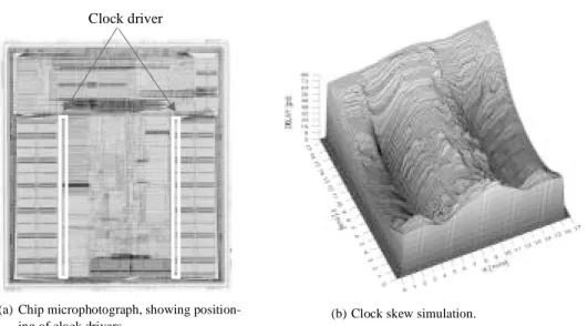
The Alpha 21064 Processor. The first generation Alpha microprocessor (21064 or EV4) from Digital Equipment Corporation used a single global clock driver [Dobberpuhl92]. The distribution of clock load capacitance among various functional block shown in Fig-ure 10.20, resulting in a total clock load of 3.25nF! The processor uses a single-phase clock methodology and the 200Mhz clock is fed to a binary fanning tree with five levels of buffering. The inputs to the clock drivers are shorted out to smooth out the asymmetry in the incoming signals. The final output stage, residing in the middle of the chip, drives the clock net. The clock driver and the associated pre-drivers account for 40% of the effective switched capacitance (12.5nF), resulting in significant power dissipation. The overall width of the clock driver was on the order of 35cm in a 0.75µm technology. A detail clock skew simulation with process variations indicates that a clock uncertainty of less than 200psec (< 10%) was achieved.
The Alpha 21164 Processor . The Alpha 21164 microprocessor (EV5) operates at a clock frequency of 300 Mhz while using 9.3 million transistors on a 16.5 mm×18.1 mm die in a 0.5 µm CMOS technology [Bowhill95]. A single-phase clocking methodology was selected and the design made extensive use of dynamic logic, resulting in a substantial clock load of 3.75 nF. The clock-distribution system consumes 20 W, which is 40% of the total dissipation of the processor.
The incoming clock signal is first routed through a single six-stage buffer placed at the center of the chip. The resulting signal is distributed in metal-3 to the left and right banks of final clock drivers, positioned between the secondary cache memory and the out-side edge of the execution unit (Figure 10.22a). The produced clock signal is driven onto a grid of metal-3 and metal-4 wires. The equivalent transistor width of the final driver inverter equals 58 cm! To ensure the integrity of the clock grid across the chip, the grid was extracted from the layout, and the resulting RC-network was simulated. A three-dimensional representation of the simulation results is plotted in Figure 10.22b. As
evi-clock driver (35cm width) ICache 373pF Integer Unit 1129pF Floating Unit 803pF Write 82pF Buffer Data 208pF Cache
dent from the plot, the skew is zero at the output of the left and right drivers. The maxi-mum value of the absolute skew is smaller than 90 psec. The critical instruction and execution units all see the clock within 65 psec.
Clock skew and race problems were addressed using a mix-and-match approach. The clock skew problems were eliminated by either routing the clock in the opposite direc-tion of the data at a small expense of performance or by ensuring that the data could not overtake the clock. A standardized library of level-sensitive transmission-gate latches was used for the complete chip. To avoid race-through conditions, a number of design guide-lines were followed including:
• Careful sizing of the local clock buffers so that their skew was minimal.
• At least one gate had to be inserted between connecting latches. This gate, which can be part of the logic function or just a simple inverter, ensures that the signal can-not overtake the clock. Special design verification tools were developed to guaran-tee that this rule was obeyed over the complete chip.
To improve the inter-layer dielectric uniformity, filler polygons were inserted between widely spaced lines (Figure 10.23). Though this may increase the capacitance to nearby signal lines, the improved uniformity results in lower variation and clock uncertainty. The dummy fills are automatically inserted, and tied to one of the power rails (VDDor GND). This technique is used in many processors for controlling the clock skew.
This example demonstrates that managing clock skew and clock distribution for large, high-performance
synchro-Figure 10.22 Clock distribution and skew in 300 MHz microprocessor (Courtesy of Digital Equipment Corporation).
Clock driver
(a) Chip microphotograph, showing position-ing of clock drivers.
(b) Clock skew simulation.
Figure 10.23 Dummy fills reduce the ILD variation and improve clock skew.
nous designs is a feasible task. However, making such a circuit work in a reliable way requires careful planning and intensive analysis.
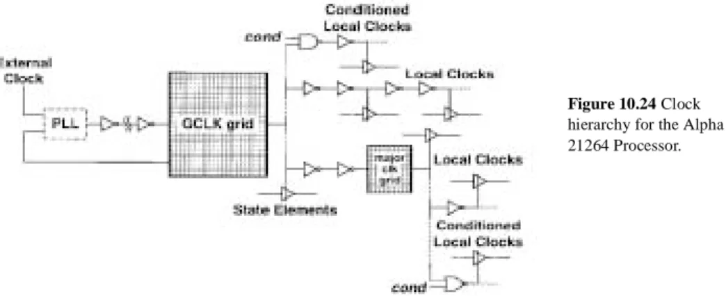
The Alpha 21264 Processor. A hierarchical clocking scheme is used in the 600Mhz Alpha 21264 (EV6) processor (in 0.35µm CMOS) as shown in Figure 10.24. The choice of a hierarchical clocking scheme for this processor is significantly different than their previous approaches, which did not have a hierarchy of clocks beyond the global clock grid. Using a hierarchical clocking approach makes trade-off’s between power and skew management. Power is reduced because the clocking networks for individual blocks can be gated. As seen in previous generation microprocessors, the clock power contributes to a large fraction of overall power consumption. Also the flexibility of having local clocks provides the designers with more freedom with circuit styles at the module level. The drawback of using a hierarchical clock network is that skew reduction becomes more dif-ficult because clocks to various local registers may go through very different paths, which may contribute to the skew. However, using timing verification tools, the skew can be managed by tweaking of clock drivers.
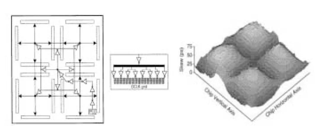
The clock hierarchy consists of a global clock grid, called GCLK, that covers the entire die. State elements and clocking points exist from 0 to 8 levels past GCLK. The on-chip generated clock is routed to the center of the die and distributed using tree structures to 16 distributed clock drivers (Figure 10.25). The global clock distribution network uti-lizes a windowpane configuration, that achieves low skew by dividing up the clock into 4 regions -- this reduces the distance from the drivers to the loads. Each grid pane is driven from four sides, reducing the dependence on process variations. This also helps the power supply and thermal problems as the drivers are distributed through the chip.
Use of a grid-ded clock has the advantage of reducing the clock skew and provides universal availability of clock signals. The drawback clearly is the increased capacitance of the Global Clock grid when compared to a tree distribution approach. Beyond the GCLK is a major clock grid. The major clock grid are used to drive different large execu-tion blocks within the chip including 1) Bus interface unit 2) integer issue and execuexecu-tion units 3) floating point issue and execution units 4) instruction fetch and branch prediction unit 5) load/store unit and 6) pad ring. The reason the major clocks were introduced was to reduce power because the major clocks have localized loads, and can be sized appropri-ately to meet the skew and edge requirements for the local loading conditions.
Figure 10.24 Clock hierarchy for the Alpha 21264 Processor.
The last hierarchy of clocks in the Alpha processor are the local clocks, which are generated as needed from any other clock, and typically can be customized to meet local timing constraints. The local clocks provide great flexibility in the design of the local logic blocks, but at the same time, makes it significantly more difficult to manage skew. For example, local clocks can be gated in order to reduce power, can be driven with wildly dif-ferent loads, and can even be tweaked to enable time borrowing between difdif-ferent blocks. Furthermore, the local clocks are susceptible to coupling from data lines as well because they are local and not shielded like the global grid-ded clocks. As a result, the local clock distribution is highly dependent on it’s local interconnection, and has to be designed very carefully to manage local clock skew.
To fully exploit the improved performance of logic gates with technology scaling, clock skew and jitter must be carefully addressed. Skew and jitter can fundamentally limit the peformance of a digital circuits. Some guidelines for reducing of clock skew and jitter are presented below.
1. To minimize skew, balance clock paths from a central distribution source to individ-ual clocking elements using H-tree structures or more generally routed tree struc-tures. When using routed clock trees, the effective clock load of each path that includes wiring as well as transistor loads must be equalized.
2. The use of local clock grids (instead of routed trees) can reduce skew at the cost of increased capacitive load and power dissipation.
3. If data dependent clock load variations causes significant jitter, differential registers that have a data independent clock load should be used. The use of gated clocks to save also results in data dependent clock load and increased jitter. In clock networks where the fixed load is large (e.g., using clock grids), the data dependent variation might not be significant.
4. If data flows in one direction, route data and clock in opposite directions. This elmi-nates races at the cost of perfomance.
Design Techniques—Dealing with Clock Skew and Jitter
5. Avoid data dependent noise by shielding clock wires from adjacent signal wires. By placing power lines (VDDor GND) next to the clock wires, coupling from neighbor-ing signal nets can be minimized or avoided.
6. Variations in interconnect capacitance due to inter-layer dielectric thickness varia-tion can be greatly reduced through the use of dummy fills. Dummy fills are very common and reduce skew by increasing uniformity. Systematic variations should be modeled and compensated for.
7. Variation in chip temperature across the die causes variations in clock buffer delay. The use of feedback circuits based on delay locked loops as discussed later in this chapter can easily compensate for temperature variations.
8. Power supply variation is a significant component of jitter as it impacts the cycle to cycle delay through clock buffers. High frequency power supply variation can be reduced by addition of on-chip decoupling capacitors. Unfortunately, decoupling capacitors require a significant amount of area and efficient packaging solutions must be leveraged to reduce chip area.
10.3.4 Latch-Based Clocking
While the use of registers in a sequential circuits enables a robust design methodology, there are significant performance advantages to using a latch based design in which com-binational logic is separated by transparent latches. In an edge-triggered system, the worst case logic path between two registers determines the minimum clock period for the entire system. If a logic block finishes before the clock period, it has to idle till the next input is latched in on the next system clock edge. The use of a latch based methodology (as illus-trated in Figure 10.26) enables more flexible timing, allowing one stage to pass slack to or steal time from following stages. This flexibility, allows an overall performance increase. Note that the latch based methodology is nothing more than adding logic between latches of a master-slave flip-flop.
For the latch-based system in Figure 10.26, assume a two-phase clocking scheme. Assume furthermore that the clock are ideal, and that the two clocks are inverted versions of each other (for sake of simplicity). In this configuration, a stable input is available to the combinational logic block A (CLB_A) on the falling edge of CLK1 (at edge2) and it has a maximum time equal to the TCLK/2 to evaluate (that is, the entire low phase of CLK1). On the falling edge of CLK2 (at edge3), the output CLB_A is latched and the computation of CLK_B is launched. CLB_B computes on the low phase of CLK2 and the output is available on the falling edge of CLK1 (at edge4). This timing appears equiva-lent to having an edge-triggered system where CLB_A and CLB_B are cascaded and between two edge-triggered registers (Figure 10.27). In both cases, it appears that the time available to perform the combination of CLB_A and CLB_B is TCLK.
However, there is an important performance related difference. In a latch based sys-tem, since the logic is separated by level sensitive latches, it possible for a logic block to utilize time that is left over from the previous logic block and this is referred to as slack borrowing [Bernstein00]. This approach requires no explicit design changes, as the pass-ing of slack from one block to the next is automatic. The key advantage of slack borrow-ing is that it allows logic between cycle boundaries to use more than one clock cycle while satisfying the cycle time constraint. Stated in another way, if the sequential system works at a particular clock rate and the total logic delay for a complete cycle is larger than the clock period, then unused time or slack has been implicitly borrowed from preceding stages. This implies that the clock rate can be higher than the worst case critical path!
Slack passing happens due to the level sensitive nature of latches. In Figure 10.26, the input to CLB_A should be valid by the falling edge of CLK1 (edge2). What happens if the combinational logic block of the previous stage finishes early and has a valid input data for CLB_A before edge2? Since the a latch is transparent during the entire high phase of the clock, as soon as the previous stage has finished computing, the input data for CLB_A is valid. This implies that the maximum time available for CLB_A is its phase time (i.e., the low phase of CLK1) and any left over time from the previous computation. For-mally state, slack passing has taken place if TCLK< tpd, A+ tpd, Band the logic functions cor-rectly (for simplicity, the delay associated with latches are ignored). An excellent quantitative analysis of slack-borrowing is presented in [Bernstein00].
Consider the latch based system in Figure 10.28. In this example, point a (input to CLB_A) is valid before the edge2. This implies that the previous block did not use up the entire high phase of CLK1, which results in slack time (denoted by the shaded area). By
Q D In CLB_A Q D D Q CLK1 L1 L2 L1 CLK2 CLK1 CLK1 CLK2 TCLK CLB_B CLB_C Q D L2 CLK2 launch A launch B compute CLB_A compute CLB_B launch C
Figure 10.26 Latch-based design in which transparent latches are separated by combinational logic. 3 2 1 4 tpd,A tpd,B tpd,C A B C Q D In Q D D Q CLK1 L1 L2 L1 CLK2 CLK1 CLB_B D Q CLB_C L2 CLK2 CLB_A
Figure 10.27 Edge-triggered pipeline (back-to-back latches for edge-triggered registers) of the logic in Figure 10.26.
construction, CLB_A can start computing as soon as point a becomes valid and uses the slack time to finish well before its allocated time (edge3). Since L2 is a transparent latch, c becomes valid on the high phase of CLK2 and CLB_B starts to compute by using the slack provided by CLB_A. CLB_B completes before its allocated time (edge 4) and passes a small slack to the next cycle. As this picture indicates, the total cycle delay, that is the sum of the delay for CLB_A and CLB_B, is larger than the clock period. Since the pipeline behaves correctly, slack passing has taken place and a higher throughput has been achieved.
An important question related to slack passing relates to the maximum possible slack that can be passed across cycle boundaries. In Figure 10.28, it is easy that see that the earliest time that CLB_A can start computing is1. This happens if the previous logic block did not use any of its allocated time (CLK1 high phase) or if it finished by using slack from previous stages. Therefore, the maximum time that can be borrowed from the previous stage is 1/2 cycle or TCLK/2. Similarly, CLB_B must finish its operation by edge4. This implies that the maximum logic cycle delay is equal to 1.5 * TCLK. However, note that for an n-stage pipeline, the overall logic delay cannot exceed the time available of n * TCLK.
Example 10.3 Slack-passing example
First consider an edge-triggered pipeline of Figure 10.29. Assume that the primary input In is valid slightly after the rising edge of the clock. For this circuit, it is easy to see that the minimum clock period required is 125ns. The latency is two clock cycles (actually, the output is valid 2.5 cycles after the input settles). Note that for the first pipeline stage, 1/2
Q D In CLB_A Q D D Q CLK1 L1 L2 L1 CLK2 CLK1 CLB_B tpd,A tpd,B
Figure 10.28 Example of slack-borrowing. CLK1 CLK2 TCLK 3 2 1 4 a b c d e tpd,A a valid b valid tDQ tpd,B c valid d valid tDQ e valid
cycle is wasted as the input data can only be latched in on the falling edge of the clock. This time can be exploited in a latch based system.
Figure 10.30 shows a latch based pipeline of the same sequential circuit. As the tim-ing indicates, exactly the same timtim-ing can be achieve with a clock period of 100ns. This is enabled by slack borrowing between logical partitions.
10.4 Self-Timed Circuit Design*
10.4.1 Self-Timed Logic - An Asynchronous Technique
The synchronous design approach advocated in the previous sections assumes that all cir-cuit events are orchestrated by a central clock. Those clocks have a dual function.
• They insure that the physical timing constraints are met. The next clock cycle can only start when all logic transitions have settled and the system has come to a steady state. This ensures that only legal logical values are applied in the next round of computation. In short, clocks account for the worst case delays of logic gates, sequential logic elements and the wiring.
• Clock events serve as a logical ordering mechanism for the global system events. A clock provides a time base that determines what will happen and when. On every Figure 10.29 Conventional edge-triggered pipeline.
D Q CL1 75ns CL2 50ns D Q CL3 75ns CL4 50ns a b d D Q c e f Out In CLK CLK CLK D Q CL1 75ns CL2 50ns CL3 75ns CL4 50ns a c In CLK D Q CLK e D Q CLK f g D Q h Out D Q CLK CLK b d CLK tpd,CL1 a valid
Figure 10.30 Latch-based pipeline.
tpd,CL2
c valid e valid f valid g valid
tpd,CL3 h valid tpd,CL4 Out valid d valid TCLK= 100ns b valid
clock transition, a number of operations are initiated that change the state of the sequential network.
Consider the pipelined datapath of Figure 10.31. In this circuit, the data transitions through logic stages under the command of the clock. The important point to note under this methodology is that the clock period is chosen to be larger than the worst-case delay of each pipeline stage, or T > max (tpd1, tpd2, tpd3) + tpd,reg. This will ensure satisfying the physical constraint. At each clock transition, a new set of inputs is sampled and computa-tion is started anew. The throughput of the system—which is equivalent to the number of data samples processed per second—is equivalent to the clock rate. When to sample a new input or when an output is available depends upon the logical ordering of the system events and is clearly orchestrated by the clock in this example.
The synchronous design methodology has some clear advantages. It presents a structured, deterministic approach to the problem of choreographing the myriad of events that take place in digital designs. The approach taken is to equalize the delays of all opera-tions by making them as bad as the worst of the set. The approach is robust and easy to adhere to, which explains its enormous popularity; however it does have some pitfalls.
• It assumes that all clock events or timing references happen simultaneously over the complete circuit. This is not the case in reality, because of effects such as clock skew and jitter.
• As all the clocks in a circuit transitions at the same time, significant current flows over a very short period of time (due to the large capacitance load). This causes sig-nificant noise problems due to package inductance and power supply grid resistance. • The linking of physical and logical constraints has some obvious effects on the per-formance. For instance, the throughput rate of the pipelined system of Figure 10.31 is directly linked to the worst-case delay of the slowest element in the pipeline. On the average, the delay of each pipeline stage is smaller. The same pipeline could support an average throughput rate that is substantially higher than the synchronous one. For example, the propagation delay of a 16-bit adder is highly data dependent (e.g., adding two 4-bit numbers requires a much shorter time compared to adding two 16-bit numbers).
One way to avoid these problems is to opt for an asynchronous design approach and to eliminate all the clocks. Designing a purely asynchronous circuit is a nontrivial and potentially hazardous task. Ensuring a correct circuit operation that avoids all potential race conditions under any operation condition and input sequence requires a careful tim-ing analysis of the network. In fact, the logical ordertim-ing of the events is dictated by the structure of the transistor network and the relative delays of the signals. Enforcing timing
Figure 10.31 Pipelined, synchronous datapath. CLK Q D In Logic Q D D Q tpd1 R1 R2 R3 Block #1 Logic Block #2 D Q R4 Logic Block #3 tpd,reg tpd2 tpd3
constraints by manipulating the logic structure and the lengths of the signal paths requires an extensive use of CAD tools, and is only recommended when strictly necessary.
A more reliable and robust technique is the self-timed approach, which presents a local solution to the timing problem [Seitz80]. Figure 10.32 uses a pipelined datapath to illustrate how this can be accomplished. This approach assumes that each combinational function has a means of indicating that it has completed a computation for a particular piece of data. The computation of a logic block is initiated by asserting a Start signal. The combinational logic block computes on the input data and in a data-dependent fashion (taking the physical constraints into account) generates a Done flag once the computation is finished. Additionally, the operators must signal each other that they are either ready to receive a next input word or that they have a legal data word at their outputs that is ready for consumption. This signaling ensures the logical ordering of the events and can be achieved with the aid of an extra Ack(nowledge) and Req(uest) signal. In the case of the pipelined datapath, the scenario could proceed as follows.
1. An input word arrives, and a Req(uest) to the block F1 is raised. If F1 is inactive at that time, it transfers the data and acknowledges this fact to the input buffer, which can go ahead and fetch the next word.
2. F1 is enabled by raising the Start signal. After a certain amount of time, dependent upon the data values, the Done signal goes high indicating the completion of the computation.
3. A Re(quest) is issued to the F2 module. If this function is free, an Ack(nowledge) is raised, the output value is transferred, and F1 can go ahead with its next computa-tion.
The self-timed approach effectively separates the physical and logical ordering functions implied in circuit timing. The completion signal Done ensures that the physical timing constraints are met and that the circuit is in steady state before accepting a new input. The logical ordering of the operations is ensured by the acknowledge-request scheme, often called a handshaking protocol. Both interested parties synchronize with each other by mutual agreement or, if you want, by shaking hands. The ordering protocol described above and implemented in the module HS is only one of many that are possible. The choice of protocol is important, since it has a profound effect on the circuit perfor-mance and robustness.
Figure 10.32 Self-timed, pipelined datapath.
R2 F2 Out In tpF2 Start Done R1 F1 tpF1 Start Done R3 F3 tpF3 Start Done
Req Req Req Req