Fabrication of thermal-isolation structure for microheater elements
applicable to fingerprint sensors
Han Ji-song
*, T. Kadowaki, K. Sato, M. Shikida
Department of Micro System Engineering, Nagoya University Chikusa, Nagoya 464-8603, Japan
Received 24 May 2001; accepted 3 April 2002
Abstract
We are developing a fingerprint-sensor device that has one-dimensionally arrayed high-density microheater elements. To provide thermal isolation, we designed and fabricated two sets of insulation cavities for the heater elements, one to reduce the heat transferring from the heater elements to the substrate and the other one to reduce that of heat to the wiring. The insulation cavities in the first set are etched and laterally penetrate under the heater bridges, leaving a SiO2diaphragm with the heater bridges on it. Those in the second set are etched lengthwise of
each heater element, leaving a set of SiO2-wiring bridges over them. These SiO2-wiring bridges are used to perform metal-film wiring. The
wiring (an electrical feed through) is formed using the lift-off method and running on the SiO2film surface from the heater element to the
bonding pad through the SiO2-wiring bridges; in this way, the amount of heat transferred to the wiring is reduced. The fabricated sensor device
was made on a (1 0 0) silicon-on-insulator (SOI) wafer using micromachining technology. Each heater bridge was 5mm17mm50mm with a pitch of 80mm. Because of its small thermal capacity and effective thermal isolation, the sensor element is very sensitive. When a 0.4 V/20ms pulse voltage was applied to the heater elements, their resistance reached a steady maximum value in about 4–5ms, i.e. the temperature rise was saturated promptly.
#2002 Elsevier Science B.V. All rights reserved.
Keywords:Micromachining; Microfabrication; Thermal insulation; Thermal-type fingerprint sensor
1. Introduction
Demands for the better ways to identify individuals are growing rapidly due to the increasing importance of infor-mation security. Though passwords are the most widely used authentication method in electronic-transaction environ-ments, they provide very weak proof of identity. Fingerprint is known to be the most representative biometrics for authentication of individuals in social information systems, and to be accepted worldwide as a proof of identity. Optical detection methods are commonly used for detecting finger-print patterns. However, optical systems need lots of com-ponents, include complex optics, such as a light source, photo diode, etc. Furthermore, their illumination systems consume a lot of power. All these make them expensive and bulky, thus prohibit their application to portable devices. Recently, thanks to MEMS technology, it has become possible to fabricate chip-based low-cost fingerprint sensors. Compared to conventional optical devices, they can be made dramatically smaller, more reliable, and robust, and would
consume less power. Therefore, it would be easy to integrate them into a wide variety of applications. They will support information-security and personal-security applications of all kinds.
Electric-capacitance and pressure-sensing type finger-print sensors have been described in several papers [1–3]. The electric-capacitance type, which is composed of a CMOS-transistor gate array, detects fingerprint patterns as a capacitance change at the gate. The pressure-sensing type, which is composed of a high-density capacitive pressure-sensor array, detects fingerprint patterns as a capacitance change at the pressure sensor. Both types are monolithic and portable, but suffer the stray capacitance noise. The electric-capacitance type also suffers the noise caused by the electric charge in a person’s body. Table 1 compares the conven-tional optical detection method and the two types of new methods mentioned above as well as our proposed thermal detection method.
We proposed a thermal-type fingerprint sensor that has robust sensing. We fabricated a prototype on a silicon-on-insulator (SOI) wafer using micromachining technology. After describing the sensing principle and fabrication pro-cess, we present some experimental results.
*
Corresponding author. Tel.:þ81-52-789-5224; fax:þ81-52-789-5032.
E-mail address:[email protected] (H. Ji-song).
0924-4247/02/$ – see front matter#2002 Elsevier Science B.V. All rights reserved.
2. Sensing principle
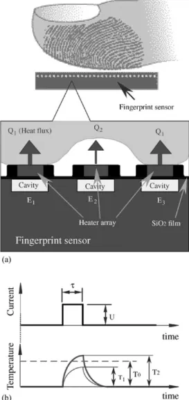
The structure and sensing principle of our sensor device are schematically shown inFig. 1. The device has arrayed-high-density microheater elements. To provide thermal iso-lation, a SiO2 film layer was used between the heater elements and substrate. A cavity is formed under each heater
bridge to reduce the heat transfer to the substrate further. When a fingertip is pressed on the sensor surface, the heater elements in contact with a fingerprint ridge, e.g. E1, will show less of a temperature rise than the elements facing to a fingerprint valley, e.g. E2, because of thermal-property differences between the ridges and valleys of the fingertip. The ridges act as heat sinks, while the valleys act as thermal insulators due to the air in the valley. If a pulse voltage is applied to each heater element, element E1will show less of a temperature rise than element E2, as sche-matically shown inFig. 1b. The temperature-rise differences between the heater elements underneath the ridges and valleys of the fingerprint can be used to reconstruct and display an image of the fingerprint patterns by means of the circuit technology.
3. Requirements
The heat produced by the input current in heater elements will be transferred in the following two directions: (1) to the atmosphere by convection and radiation and (2) to the substrate and wiring by conduction. As a component of the fingerprint sensor, the temperature of the heater elements will not be very high, so, it is reasonable to ignore the heat loss by radiation. As described above, the proposed sensor works by using the temperature-rise differences between elements E1and E2to detect clear fingerprint patterns. To develop a practical device, we need to reduce the amount of heat transferred to the substrate and wiring, so that the heat produced in the heater elements could be transferred mainly to the atmosphere. There have been many papers concerning the thermal-isolation structures [4–20] to reduce the heat transferring from the heater to the substrate, but no one has mentioned about the thermal isolation to reduce the heat transferring from the heater to the wiring. In this paper, we focus attention on the methods to reduce the heat transfer-ring to the substrate and witransfer-ring.
3.1. Reduce heat transfer to substrate
To reduce the heat transferring to the substrate, three type of thermally isolated structures are widely used in the Si-based thermal-type microsensors, i.e. the cantilever type
Table 1
Comparison among different types of fingerprint sensors
Type Components Advantages Problems to solve
Optical LDa, PDa, prism, and glass plate Established method Large size
Pressure sensing Micropressure sensor array Monolithic, portable Stray capacitance noise
(in case of capacitance-type sensor) Electric capacitance CMOS-transistor gate array Monolithic, portable Stray capacitance noise, electric
charge in human body Heat capacitance (thermal type) Microheater array Monolithic, portable, robust sensing Packaging, multilayer wiring
a
LD, laser diode; PD, photo diode.
Fig. 1. Fingerprint sensor with arrayed microheater elements: (a) device structure; (b) sensing principle.
[4–6], the backside etched diaphragm type[7–12]and front-side etched micro-air-bridge or floating membrane type
[13–21]. The cantilever-type structure is not suitable to the thermal-type fingerprint sensor because of the unwanted big deformation when the fingertip is touching on it. The backside-etched diaphragm is a planar structure and has high mechanical strength, but thermal properties of this structure are rather inferior[18]. The backside etched diaphragm-type structure makes the microheater has bigger thermal capacity and thermal conductance, so that to cut down its sensitivity
[21], furthermore, this kind of structure makes the sensor element difficult to downsize [17] when considering the high-density sensor array for the applicable fingerprint sensors. The reported front-side etched micro-air-bridge and floating membrane types[13–21]have the advantages of small size, high sensitivity, quick response and low power consumption, but their sizes are not small enough to be applied to the thermal-type fingerprint-sensor array. For a fingerprint sensor, the sensitive matrix need to include 300– 500 dpi of sensors[22], in order to detect clear fingerprint patterns. For this purpose, we developed a micro-air-bridge type high-density (80mm of pitch distance) microheater array. The cavities underneath each heater bridge were laterally penetrated.
Figs. 2 and 7 show the structure of the cavity and diaphragm for the proposed sensor device. In the fabrication,
we used a P-type (100) SOI wafer as the starting material. The wafer had a 400mm thick substrate and a 5mm thick top layer of (1 0 0) silicon, sandwiching a 1mm thick SiO2 insulation layer. The direction of the orientation flat was
h1 1 0i, both in the substrate and top layer, and the resistivity of the top-layer silicon was 5Ocm.
The diaphragm underneath each heater bridge was fab-ricated as follows. After making an array of microheater elements on the top layer of the SOI wafer, the substrate was etched further by photolithography and anisotropic etching with a TMAH solution from the front-side rectangular mask-aperture whose orientation was rotated 458from theh1 1 0i
orientation flat. Appropriately sized cavity-etching windows and pitch were used to etch laterally penetrated cavity underneath each heater bridge.
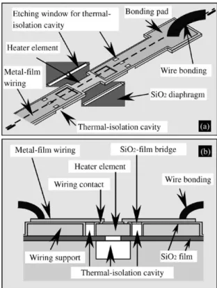
3.2. Reduction heat transfer to wiring
To reduce the heat transferring to the wiring, we used the thin metal-film wiring. The electrical feed through of the wiring (Fig. 2) can be made by physical-vapor-deposition (PVD) or sputtering. We used the method of sputtering. Each heater element was 5mm thick which makes it difficult to form such a thin metal film that completely covering the heater-element steps, due to the poor coverage of deposited film on the step walls. To avoid open circuits on the steps, we used the wiring-support structure as shown inFig. 3. Each heater element was separated from the wiring-support struc-ture by a thermal insulation cavity. Over each cavity is a
Fig. 2. Structure of cavity and diaphragm: (a) top view; (b) cross-sectional view.
Fig. 3. Proposed sensor element structure: (a) top view; (b) cross-sectional view.
SiO2-film bridges for the wiring (electrical feed through). The cavity and SiO2-film bridges were made by photolitho-graphy and anisotropic etching with a TMAH solution from rectangular mask apertures whose orientations were rotated 458from theh1 1 0iorientation flat. An appropriately sized cavity-etching windows and pitch were used to etch the laterally penetrated cavity underneath each SiO2film bridge. The heater and wiring-support surface were thermally oxidized before fabricating the electrical feed through. The feed through was made of a thin metal film using the lift-off method and formed on the SiO2-film surface. It ran from the heater element to the bonding pad (Fig. 3). In this way, the heat transferring to the bonding pad and wiring was reduced.
3.3. Structure analysis
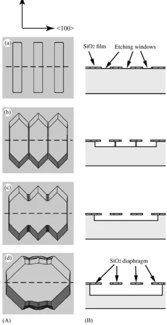
Before starting the fabrication process, we analyzed the structure of our device by simulation. Fig. 4 shows the fabrication sequence for the cavity and diaphragm structure.
Fig. 4Ashows the top views generated by 3-D calculations, andFig. 4Bshows the cross-sectional views. The fabrica-tion sequence was analyzed using MICROCAD, a 3-D etching simulator co-developed by the Fuji Research Insti-tute Corporation and Nagoya University[23]. It is equipped with a database of orientation-dependent etching rates for single-crystal silicon. An appropriately sized etching-win-dow pattern was arrayed on the SiO2film with an appro-priate pitch distance (Fig. 4a), and the silicon underneath the SiO2mask was anisotropically etched by undercutting using KOH or TMAH etching solution. The etching was stopped by the (1 1 1) surface (Fig. 4b). Further etching creates a laterally penetrated cavity, resulting in the dia-phragm structure (Fig. 4c and d). Based on our simulation results, we developed a process for fabricating the proposed sensor device.
4. Fabrication process
Fig. 5shows the schematic drawings of the fabrication process.Fig. 5Ais top views andFig. 5Bis cross-sectional views. As described above, a (1 0 0) SOI wafer was used as the starting material: (a) to make the heater and wiring-bridge patterns, the wafer surface was thermally oxidized to a thickness of 1.5mm at a temperature of 10008C (Fig. 5a); (b) the wiring-bridge and etching-window patterns were formed by etching the SiO2film to a thickness of 1.2mm with BHF (50% HF: 40% NH3F¼1: 6;Fig. 5b); (c) the heater-element patterns and etching windows for the ther-mal-isolation cavity under the wiring bridges were formed by etching the 0.3mm thick SiO2 film (Fig. 5c); (d) the wiring bridges, 5mm thick heater elements and wiring supports were formed by etching the Si top layer with TMAH solution (25 wt.%, 808C;Fig. 5d); (e) after etching out the 0.3mm thick SiO2 film on the heater surface,
51015 atoms/cm2 of boron were doped into the heater elements to reduce their electrical resistivity from 5 to 0.02Ocm (Fig. 5e); (f) a 0.5mm thick SiO2etching mask was formed on the top-layer silicon (heater and wiring support) surface by another thermal oxidization at 10008C (Fig. 5f); (g) the wiring-contact windows for the heater elements and etching windows for the thermal-iso-lation cavities were formed by etching the SiO2film with BHF (Fig. 5g); (h) the thin metal-film wiring was formed by sputtering 0.02mm thick Cr followed by 0.37mm thick Au (Fig. 5h); when sputtering 0.1mm thick Al followed by 0.37mm thick Au instead of sputtering Cr/Au, the metal film was taken off in KOH or TMAH solution (Fig. 6); (i) the
Fig. 4. Fabrication sequence for a cavity and diaphragm structure analyzed by MICROCAD: (A) top views from 3-D calculations; (B) cross-sectional views.
laterally penetrated thermal-isolation cavities were formed by etching the substrate with TMAH solution (Fig. 5i).
SEM photos of the fabricated high-density heater-elements array having Cr/Au metal-film wiring are shown inFig. 7. Each heater bridge was 5mm17mm50mm with a pitch of 80mm and a laterally penetrated cavity underneath it. After sputtering the Cr/Au for the wiring, each wiring bridge was 1:89mm5mm35mm with a laterally penetrated cavity underneath it.Fig. 8shows the state of the wire bonding, and
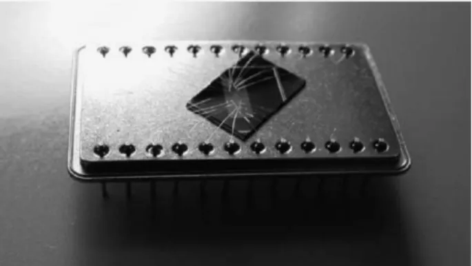
Fig. 9shows the wire bonded sample chip for experiment.
5. Experimental results
5.1. TCR of heater elements
The temperature coefficient of resistor (TCR) of the heater element was obtained by the actual measurement of the resistance variation with the slowly increased tem-perature in a precise resistive oven. Fig. 10 shows the detection circuit and schematic illustration of the experi-mental set-up.Rsis the standard electrical resistance, andRh
is the microheater element’s electrical resistance. A rectan-gular type pulse voltageU1was applied to detect TCR of the heater elements. In order to avoid the effect of heat produced by the heater itself due to the input power, it is necessary to make the U1as small as possible. During the temperature rise in oven, the input pulse voltageU1is constant and the standard electrical resistanceRsis also constant. Because,Rh is changing with the surrounding temperature, the voltage ratioU2/U1will change. By measuring the voltageU1andU2 at the same time with two-channel digital-oscilloscope,Rh could be calculated. Rh¼ U2 U1U2 Rs (1)
Figs. 11 and 12 show the temperature dependence of the heater elements’ resistance detected by circuit shown in
Fig. 10. The experimental results were got from the samples which, respectively with and without doping boron impurity. In our experiment, during the temperature change from 18 to 508C, the TCR of the heater element dropped 0.0233/8C when no doping with boron impurity; and from 14 to 1808C, the TCR rose linearly about 1:988103/8C when 51015 atoms/cm2 of boron is doped. By adjusting the dopant concentration, the resistivity of silicon and its TCR could be easily controlled[24–27]. As a thermal-type fingerprint sensor, it is favorable to possess higher value of TCR for its sensitivity. The following experimental results were got from the non-boron doped samples.
5.2. Thermal properties
5.2.1. Effect of wiring-bridge structure
Because the TCR of the heater elements was changing with the temperature (seeFig. 11), at the same input voltage U1, the outputU22/Rhbetween the two kind of structures that with and without wiring bridge was different. In order to make it easier to compare the thermal properties among the
different structures, a DC current was applied to the detecting circuit.Fig. 13shows the resistance ratio change against the input current at the surrounding temperature of 188C for the three different sensor structures. Comparing to the structure (a), structure (b) and (c) showed sharper decrease in the
Fig. 6. Al/Au wiring film is taken off in KOH or TMAH solution.
Fig. 7. SEM photos of fabricated heater-element array with Cr/Au metal-film wiring: (a) magnified view of wiring bridge; (b) fabricated microheater array; (c) magnified view of microheater element with cavity underneath.
heater resistance change, owing to the effects of thermal-isolation wiring-bridge structure and the smaller thermal capacity. In both structures, the heater resistance showed sharp decrease, according to the increase in input current. However, it trends to a constant in a high current region. In other words, it means that the heater temperature increased dramatically at beginning, and then trends to its balanced state. The reason is supposed to be as follows. At the low current region, the heat produced by the input current was used mainly to increase the temperature of the heater itself
and made the heater temperature rise dramatically. Along with the further increase of input current, one part of the heat will be used to increase the heater temperature and the other part of that will be transferring to the surrounding materials, including the substrate, wiring and the surrounding air, so that the heater resistance change became slowdown. When the temperature of the heater element reached some extent, among the heat produced by the input current and those transferring to the heater, substrate and surrounding air as well as the wiring will be reached a thermal balance, so that the temperature of the heater element became a constant. From the experimental results, it was known that at the near
Fig. 8. Bonding pad: (a) after wire bonding; (b) before wire bonding.
Fig. 9. Wire bonded sample chip for experiment.
Fig. 10. Experimental set-up: (a) detection circuit; (b) schematic illustration of experimental set-up.
Fig. 11. Electrical resistance-ratio of the heater element vs. applied temperature, when there is no doping with boron impurity.
point of the input current 0.3 mA, the temperature change of the heater element became slowdown and near the 2.25 mA, the heater temperature trends to a constant. According to the experiment of TCR, the heater temperature was about 60 and 808C, respectively in the sensor structure of (a) and (b) at their balanced states. By means of the wiring-bridge struc-ture, about 208C of temperature rise was got in our sensor samples.
5.2.2. Effect of cavity under the heater elements
FromFig. 13, it was known that between the structures with and without cavity under the heater element showed only slight differences in the thermal properties. We suppose the following points may be the main reason: (1) the cavity under the heater element was not deep enough (depth: 38– 40mm), so that the heat was transferring from the heater to the Si substrate through the air layer in the cavity; (2) both ends of the heater were located on the substrate and the heat was lost through the SiO2layer to the Si substrate.
In order to get better thermal isolation results, it is important to make deeper cavity and thicker insulation layer between the heater and Si substrate.
5.3. Thermal response
Fig. 14shows one of the experimental results of the time response on the proposed sensor device. The detecting circuit was same toFig. 10, except that the sensor sample was not in the oven but in the atmosphere. The structure of the sample was same toFig. 13c, and the experiments were carried out in the room temperature of 188C. Along with the increase of the input pulse voltageU1,U2will increase. But, the voltage ratioU2/(U1U2) will decrease because of the negative TCR of Rh. In experiment, it was found that the proposed sensor element showed quick response in tem-perature rise and the bigger the input voltage, the shorter the response time. As shown inFig. 14, when a 0.4 V/20ms of pulse voltage U2 was applied to the heater elements, its steady maximum value can be reached in about 4–5ms on the heater elements. According to the CTR, it is known that the temperature on the heater element was risen from the room temperature of 188C to the near 288C.
This fact shows that the heater element was thermally isolated from environment, as well as that the heat capacity is small enough. Such a structure will be useful in a variety of thermal sensors such as temperature sensors, micro-flow sensors, in addition to the thermal-type fingerprint sensors.
6. Summary
We proposed a thermal-type fingerprint sensor, from the standpoint of its robustness in sensing. We developed a fabrication process for the proposed device and successfully fabricated one-dimensionally arrayed high-density micro-heater elements on a (1 0 0) SOI wafer. Each micro-heater bridge was 5mm17mm50mm and had a pitch distance of 80mm. Heater elements were thermally insulated from the substrate by a 1mm thick SiO2 layer and a laterally penetrated cavity underneath each heater bridge. But, 40mm
Fig. 13. Relationship between input current in the heater element and its resistance change.
Fig. 12. Electrical resistance-ratio of the heater element vs. applied temperature, when boron impurity is doped.
Fig. 14. Experimental result of the quick time response on the heater elements. Picture is got from the digital oscilloscope output wave. When a 20ms of pulse voltageU1is applied to the detection circuit, the voltage on the heater element reached its steady valueU2in about 4–5ms.
of depth in cavity and 1mm thick SiO2layer was not enough for effective thermal isolation.
Because of its small thermal capacity and effective ther-mal isolation, the wiring-bridge structure is effective for its sensitivity in the thermal-type sensors. By means of a SiO2 wiring-bridge structure, about 208C of temperature rise was got in our sensor samples comparing to the structure that without wiring-bridge, and about 108C of temperature rise was possible in 4–5ms of time at a 0.4 V/20ms of pulse voltage.
Such a thermal-type sensor structure may thus be useful for a variety of thermal sensor applications, such as micro-temperature sensors and microflow sensors, in addition to the thermal-type fingerprint sensors. We plan to improve the thermal isolation effect further by means of the appropriate insulation layer between the heater and the substrate.
References
[1] S. Jung, C. Hierold, T. Scheiter, P.W. von Basse, R. Thewes, K. Goser, W. Weber, Intelligent CMOS fingerprint sensors, in: Proceedings of the Transducers’99, Sendai, Japan, June 1999, pp. 966–969. [2] R.J. De Souza, K.D. Wise, A very high density bulk micromachined
capacitive tactile imager, in: Proceedings of the Transducers’97, June 1997, pp. 1473–1476.
[3] P. Rey, P. Charvet, M.T. Delaye, S. Abowhassan, A high density capacitive pressure sensor array for fingerprint sensor application, in: Proceedings of the Transducers’97, June 1997, pp. 1453–1456. [4] B.H. Kim, F.E. Prins, D.P. Kern, S. Raible, U. Weimar,
Multi-component analysis and prediction with a cantilever array based gas sensor, Sens. Actuators B 78 (2001) 12–18.
[5] F. Vo¨lklein, G. Min, D.M. Rowe, Modelling of a microelectrome-chanical thermoelectric cooler, Sens. Actuators A 75 (1999) 95–101. [6] H. Baltes, O. Paul, O. Brand, Micromachined Thermally Based CMOS
Microsensors, IEEE, Vol. 86, No. 8, August 1998, pp. 1660–1678. [7] K.-H. Lee, H.-K. Lee, H.-J. Byun, I.-J. Cho, J.-U. Bu, E. Yoon, An
audio frequency filter application of micromachined thermally-isolated diaphragm structures, Sens. Actuators A 89 (2001) 49–55. [8] F. Solazbacher, C. Imawan, H. Steffes, E. Obermeier, A new low
power SiC/HfB2-based microhotplate with integrated IDC for metal oxide gas sensors, in: Proceedings of the Tranducers’99, Sendai, Japan, 1999, pp. 1032–1035.
[9] I. Simon, M. Arndt, Thermal and gas-sensing properties of a micromachined thermal conductivity sensor, in: Proceedings of the Transducers’01 Eurosensors, Vol. XV, 2001, pp. 1492–1495. [10] S. Okano, S. Hirano, H. Horiguchi, An analysis of the heat transfer for
a micro-flow sensor, T. IEE Japan, Vol. 119E, No. 1, 1999, pp. 38–43. [11] Y. Ariyoshi, K. Tanimoto, E. Yoshikawa, T. Usami, Development of Simulator for Heat Transfer Characteristic of Microheater, MM-99-29, 1999, pp. 1–6.
[12] F. Sato, T. Nimura, M. Shiinoki, S. Yoshida, Development of a Multiple-point-measurement Type Flow Meter with Thermal Flow Sensors, PS-97-7, 1997, pp. 37–43.
[13] J.-I. Hayasaka, C. Sawai, M. Kimura, Study on Ultraminiature Thermal Analysis Device with Micro-air-bridge Heater and a New Method for its Heating-Rate Curve, T. IEE, Vol. 119E, No. 3, Japan, 1999, pp. 119–124.
[14] H. Wado, T. Yamamoto, Y. Takeuchi, Analysis of Heat Transfer in Micro-bridge Heater, MM-99-6, 1999, pp. 1–4.
[15] M. Nagata, M. Stevens, N. Swart, T. Dravia, A. Nathan, Optimization of two-element flow microsensors using quasi 3-D numerical electrothermal analysis, Sens. Actuators A 90 (2001) 102–110.
[16] S.-T. Hung, S.-C. Wong, W. Fang, The development and application of microthermal sensors with a mesh-membrane supporting structure, Sens. Actuators A 84 (2000) 70–75.
[17] T. Neda, K. Nakamura, T. Takumi, A polysilicon flow sensor for gas flow meters, Sens. Actuators A 54 (1996) 626–631.
[18] Y. Mo, Y. Okawa, M. Tajima, T. Nakai, N. Yoshiike, K. Natukawa, Micro-machined gas array based on metal film microheater, Sens. Actuators B 79 (2001) 175–181.
[19] M. Kimura, M. Yoshida, N. Suzuki, Schottky Barrier Thermistor on the Micro-air-bridge, in: Proceedings of the 7th International Conference on Solid-State Sensors and Actuators Transducers’93, June 7–10, 1993, Pacifico, Yokohama, Japan, pp. 746–749. [20] S. Kodato, Q. Zhuaug, High-power Si-microbridge infrared light
source, in: Proceedings of the Transducers’99, Sendai, Japan, June 1999, pp. 582–585.
[21] M. Furuya, S. Fujiwara, M. Kimura, Miniature Thermal Analysis Sensor Using Microheaters on SOI Substrate, PHS-00-16, pp. 1–4. [22] http://www.kinetic.bc.ca/Biometrics/sensor-comparison.html#f. [23] K. Sato, K. Asaumi, G. Kobayashi, Y. Iriye, Development of an
Orientation-Dependent Anisotropic Etching Simulation System MICROCAD, Electronics and Communications in Japan, Part 2, Vol. 83, No. 4, 2000, 13–22.
[24] J.Y.W. Seto, Piezoresistive properties of polycrystalline silicon, J. Appl. Phys. 47 (1976) 4780–4783.
[25] W.R. Runyan, Silicon Semiconductor Technology, McGraw-Hill, New York, 1965.
[26] G. Bertolini, A. Coche, Semiconductor Detectors, North-Holland, Amsterdam, 1968.
[27] H.F. Wolf, Silicon Semiconductor Data, Pergamon Press, New York, 1969.
Biographies
Han Ji-song received his BEng. and MEng. from Jilin University of Technology, China, in 1984 and 1987, respectively. Since 1987, he had been working in the Automobile Institute of Technology Chang-chun, China. He is now a doctoral course student in Department of Micro System Engineering, Nagoya University, Japan. He is a member of the Institute of Electrical Engineers of Japan, and the Japan Society of Mechanical Engineers.
Tadashi Kadowaki received his B.S. (mechanical engineering) and MS degrees from Nagoya University, Japan in 1998 and 2000, respectively. He is currently working at Matsushita Electronic Components Co. Ltd. and researching micromachine and microfabrication.
Kazuo Sato received his B.S. degree (mechanical engineering) from Yokohama National University in 1970 and a PhD from the University of Tokyo in 1982. In 1970, he joined Hitachi Ltd., Tokyo. He has been engaged in researching micromachining technologies and their applications since 1983. Since 1994, he has been a professor at Nagoya University. Dr. Sato is a member of the Japan Society of Mechanical Engineers, the Japan Society for Precision Engineering, the Institute of Electrical Engineers of Japan, and the Japan Society for Technology of Plasticity.
Mitsuhiro Shikida received his B.S. and M.S. degrees in electrical engineering from Seikei University, Tokyo, in 1988 and 1990, respectively. He received his PhD from Nagoya University in 1998. From 1990 to 1995, he worked at Hitachi, Ltd., Tokyo. In 1995, he joined the Department of Micro-System Engineering at Nagoya University as a research associate. He has been an assistant professor since 1998, and joined the Research Center for Advanced Waste and Emission Management at Nagoya University in 2001. His research interests include microactuators, microfabrication, and micromechanical structures. Dr. Shikida is a member of the Institute of Electrical Engineers of Japan and the Japan Society of Mechanical Engineers.