Hardness of Electrodeposited Nano-Nickel Revisited
by
Bill Tsz Fai Tang
A thesis submitted in conformity with the requirements for the degree of Master of Applied Science Department of Materials Science and Engineering
University of Toronto
ii
Hardness of Electrodeposited Nano-Nickel Revisited
Bill Tsz Fai TangMaster of Applied Science
Department of Materials Science and Engineering University of Toronto
2011
Abstract
In the past, hardness measurements on nanocrystalline metals were limited to Vickers
micro-hardness and nano-indentation tests, mainly due to sample size/thickness limitations. On the
other hand, most industries require hardness values on the Rockwell scale and make extensive
use of hardness conversion relationships for various hardness scales. However, hardness
conversions currently do not exist for nanocrystalline metals. With recent advances in
electrodeposition technology, thicker specimens with a wide range of grain sizes can now be
produced. In this study, the relationships between Vickers and Rockwell hardness scales have
been developed for such materials. In addition, hardness indentations were used to gain further
insight into the work hardening of nanocrystalline and polycrystalline nickel. Vickers
microhardness and nano-indentation profiles below large Rockwell indentations showed that
polycrystalline nickel exhibited considerable strain hardening, as expected. On the other hand,
for nanocrystalline nickel the micro-Vickers and nano-indentations hardness profile showed low
iii
Acknowledgements
I would like to express my sincerest thanks to my supervisor, Professor Uwe Erb, who
provided me with guidance and patience, along with a sense of humour which made the
experience enjoyable. I would also like to thank Mr. Iain Brooks of Integran Technologies, Inc
for providing the materials needed for this research and Dr. Gordana Cingara for her TEM work.
Financial support from the Natural Sciences and Engineering Research Council of
Canada, the Ontario Research Fund and the University of Toronto Open Fellowship are also
gratefully recognized.
Most importantly, I would like to thank the most important people in my life – my family
and my girlfriend, Winnie Luy. Their faith in me and support had made everything possible. I
iv
Table of Contents
Abstract ... ii
Acknowledgements ... iv
List of Tables ... vii
List of Figures ... viii
Chapter 1: Introduction ... 1
Chapter 2: Literature Review ... 5
2.1 Synthesis of Nanocrystalline Materials ... 5
2.1.1 Solid State Processing ... 5
2.1.1.1 Equal-Channel Angular Pressing (ECAP)……….6
2.1.1.2 Mechanical Attrition………..……….6
2.1.2 Vapour Phase Processing ... 9
2.1.3 Crystallization of Amorphous Precursors ... 11
2.1.4 Electrochemical Processing ... 11
2.2 Characteristics Structure of Nanomaterials ... 14
2.3 Properties of Electrodeposited Nanocrystalline Materials ... 16
2.3.1 Mechanical Properties of Nanocrystalline Materials ... 17
2.4 Deformation Mechanisms in Nanocrystalline Materials ... 18
2.4.1 Grain Boundary Sliding and Grain Rotation ... 19
2.4.2 Nabarro-Herring Creep ... 23
2.4.3 Coble Creep ... 24
2.5 Strain Hardening in Polycrystalline and Nanocrystalline Materials ... 25
2.6 Hardness ... 31
2.6.1 Rockwell and Superficial Rockwell Hardness ... 32
2.6.2 Brinell Hardness ... 33
2.6.3 Vickers and Knoop Hardness ... 34
v
2.6.5 Summary of Hardness Tests ... 37
2.7 Hardness Conversion Relationship ... 38
2.8 Objectives of this Research ... 38
Chapter 3: Materials and Experimental Methods ...40
3.1 Materials and Sample Preparation ... 40
3.2 Materials Characterization ... 42
3.2.1 Energy-Dispersive X-ray Spectroscopy (EDX) ... 42
3.2.2 Grain Size Analysis ... 42
3.2.2.1 Transmission Electron Microscopy (TEM)……….….42
3.2.2.2 Optical Imaging of Polycrystalline Microstructure.………...….43
3.3 Mechanical Testing ... 43
3.3.1 Rockwell Hardness Testing ... 43
3.3.2 Vickers Micro-hardness Testing ... 44
3.3.3 Nanoindentation Hardness Testing ... 44 Chapter 4: Results and Discussion ...45
4.1 Characterization of Materials ... 45
4.1.1 Grain Size Analysis ... 45
4.1.2 EDX Analysis ... 55
4.2 Vickers Micro-hardness ... 56
4.3 Rockwell and Superficial Rockwel Hardness ... 58
4.4 Relationship between Vickers and Rockwell Scales ... 61
4.5 Strain Hardening Capacity ... 67
Chapter 5: Conclusion ...79
Chapter 6: Recommendation for Future Work ...81
Chapter 7: References ...82
vi
List of Tables
Table 2.1: Upper and lower limits for critical distance between two dislocations [modified after Wang (1994)].
Table 2.2: Summaries of the static hardness indentation tests
Table 4.1: Average grain sizes of the specimen used in this experiment
Table 4.2: Compositsion of the materials in weight percentage, as determined by energy-dispersive X-ray spectroscopy analysis
Table 4.3: Average Vickers Micro-hardness measurements Table 4.4: Average Rockwell hardness measurements
Table 4.5: Average Superficial Rockwell hardness measurements Table 4.6: Vickers to Superficial Rockwell Hardness Relationships Table 4.7: Vickers to Rockwell Hardness Relationships
vii
List of Figures
Figure 2.1: (a) Schematic representation of ECAP [Komura et al. (1999)], (b) the four processing routes for ECAP, rotation between each pass [Iwahashi et al. (1998)]
Figure 2.2: (a) Schematic representation of mechanical attrition [Fecht, (1990)], (b) Schematic representation of the consolidated structure [Birringer et al. 1988]
Figure 2.3: Schematic drawing of a inert gas condensation synthesis technique [Siegel et al. (1989)]
Figure 2.4: Schematic of an electrodeposition set up [Cheung (2001)]
Figure 2.5: Schematic diagram of (a) Diffusion processes on the surface of the specimen and (b) the Nernst diffusion layer [Erb et al. (2007)]
Figure 2.6: Schematic diagram of the atomic arrangement in nanocrystalline materials. The black circles represent the ordered structure, the grains; the white circles represent the disordered structure, the intercrystalline component [Gleiter (1989)].
Figure 2.7: (a) The 14- sided tetrakaidecahedron grain shape, [Allen and Thomas (2003)] and (b) the volume fractions of total intercrystal components (Vic), grain boundary (Vgb) and triple junctions (Vtj) as a function of grain size, [Palumbo et al. (1990)]
Figure 2.8: Plot of Vickers micro-hardness against one over square root of grain size, [Armstrong et al. (1896)]
Figure 2.9: Low temperature deformation mechanisms in nanocrystalline metals, from [Erb et al. (2004)]
Figure 2.10:Schematic diagram of a) grain boundary sliding with a protrusion in the boundary, b) grain boundary sliding of the triple junction, Gifkins and Snowden [1966]
viii
Figure 2.12: Schematic diagram of grain rotation of nanocrystalline material under tensile loading due to disclination dipole motion, as proposed by Ovid'ko [2002]
Figure 2.13: Nabarro-Herring vacancy diffusion mechanism through a grain during loading, Herring [1949]
Figure 2.14: Coble vacancy diffusion mechanism along grain boundary during loading, Ashby [1969]
Figure 2.15: The strain hardening behaviour of copper, brass and steel increase in tensile strength with increase in cold work [Callister (2005)].
Figure 2.16: Plot of Vickers micro-hardness against elongation for as-received and cold-rolled polycrystalline nickel [Liang and Yu, (2008)]
Figure 2.17: Plot of Vickers micro-hardness against elongation for as-received and cold rolled polycrystalline and nanocrystalline nickel [Zabev, (2008)]
Figure 2.18: Plot of yield strength against rolling strain, where yield strength is determined by one third of Vickers micro-hardness relationship [Wu et al. (2009)]
Figure 2.19:Schematic diagram of the cross section of Rockwell hardness measurement, modified [ASTM E18 – 08, (2008)]
Figure 2.20:Schematic diagram of the indenter and indentation of Vickers and Knoop hardness [Callister (2005)].
Figure 2.21: Schematic diagram of the Berkovich indenter
Figure 3.1: Schematic diagram of the cross section below the Rockwell indentation. Vickers micro-hardness profiles were measured along direction x.
Figure 4.1: Optical micrograph of polycrystalline nickel, Ni 1
ix
Figure 4.3: Plot of frequency against grain size for the polycrystalline nickel (Ni 1) with superimposed log-normal distribution
Figure 4.4: Plot of cumulative volume fraction against grain size for the polycrystalline nickel, Ni
Figure 4.5: Bright field TEM image, dark field, TEM image and SADP of ultra-fine grained nickel sample, Ni 4
Figure 4.6: Grain size distribution histogram for ultra-fine-grained nickel, Ni 4
Figure 4.7: Plot of frequency against grain size for the ultra-fine-grained nickel (Ni 4) with superimposed log-normal distribution.
Figure 4.8: Plot of cumulative volume fraction against grain size for the ultra-fine-grained nickel, Ni 4
Figure 4.9: Bright field TEM image, dark field, TEM image and SADP of nanocrystalline nickel sample, Ni 6
Figure 4.10: Grain size distribution histogram for nanocrystalline nickel sample, Ni 6
Figure 4. 11:Plot of frequency against grain size for nanocrystalline nickel sample (Ni 6) with superimposed log-normal distribution
Figure 4.12: Plot of cumulative volume fraction against grain size for nanocrystalline nickel sample, Ni 6
Figure 4.13: Vickers hardness plotted against grain size
Figure 4.14:Hardness plotted against d-0.5 a) Rockwell, b) Superficial Rockwell Ball indenter and c) Superficial Rockwell Diamond indenter
Figure 4.15: Experimental results and ASTM relationship of Vickers Micro-hardness plotted against a) Superficial Rockwell, Ball indenter, b) Superficial Rockwell, Diamond indenter, c) Rockwell, Ball indenter and d) Rockwell, Diamond indenter
Figure 4.16: Optical micrographs of the cross sections of Rockwell indentations in a) Ni 1, Diamond indenter, b) Ni 1, Ball indenter, c) Ni 5, Diamond indenter, d) Ni 5, Ball indenter, e) Ni 6, Diamond indenter and f) Ni 6, Ball indenter
x
Figure 4.17: Vickers micro-hardness as a function of distance from the Rockwell Diamond indentation
Figure 4.18: Vickers micro-hardness as a function of distance from the Ball indentation
Figure 4.19:Normalized hardness as a function of distance from Rockwell indentation, under Rockwell Diamond indentations
Figure 4.20:Normalized hardness as a function of distance from Rockwell indentation, under Rockwell Ball indentations
Figure 4.21:Optical micrographs of the cross sections of Rockwell Diamond indentation in Ni 6
Figure 4.22:Normalized nanoindentation hardness as a function of distance from Rockwell indentation against under Rockwell Diamond indentation
1
1.0 Introduction
Nanocrystalline metals are defined as metals with grain sizes less than 100 nm. These materials
have drawn considerable industrial and academic interest due to the substantial improvements of
certain properties. Extensive research has shown that with the reduction in grain size properties
such as strength [e.g. Nieman et al. (1990)], wear rate [e.g. Jeong (2003)], magnetic coercivity
[Herzer et al. (1989)], corrosion behaviour [e.g. Rofagha et al. (1991)] and hardness [e.g. Gleiter
(1989)] are greatly enhanced and surpass the properties observed in the larger grained,
polycrystalline materials.
Many different synthesis techniques for the production of nanocrystalline materials have been
developed over the past three decades. These synthesis techniques include severe plastic
deformation [e.g Valiev et al. (1999)], physical vapour deposition [e.g Iwama et al. (1992)],
chemical vapour deposition [e.g Gleiter (1981)], sputtering [e.g Grovenor et al. (1984)],
crystallization of amorphous materials [e.g Herzer (1995)], inert gas condensation [e.g Gleiter
(1981)], electrodepostion [e.g McMahon and Erb (1989)], etc. Each method uses different
mechanisms to create the nanocrystalline structure such that the internal porosity, impurity
content and grain boundary structure formation of the end product may differ considerably from
one technique to another. Hence, by fabricating nanocrystalline materials with different
2
A previous study by Palumbo et al. has shown that through grain refinement (reducing the size of
an idealized 14- sided tetrakaidecahedron as the grain shape model) to the nanocrystalline
regime, the total intercrystal volume (sum of grain boundaries and triple junctions) can increase
to a significant fraction of the total material volume [Palumbo et al. (1990)]. For example, this
increase in interfacial volume fractions is an important aspect in interpreting many mechanical
properties of nanocrystalline materials, as deformation mechanisms in nanocrystalline materials
are quite different than in polycrystalline materials. Several known deformation mechanisms in
nanocrystalline materials at low temperature are operative in polycrystalline materials only at
high stress or high temperatures. These include: grain rotation, grain boundary sliding, Coble
creep and Nabarro-Herring creep. Since grain size, grain boundary structure and secondary
defects (e.g. porosity, impurities) all play a major role in deformation mechanisms, the synthesis
technique can have a significant influence on the performance of nanomaterials under plastic
deformation conditions.
It is well established that the hardness and strength of metals increase with the refinement of
grain size to the nanocrystalline regime. This behaviour is the well known classical Hall-Petch
behaviour [Hall (1951), Petch (1953)]. In the past, hardness measurements for nanocrystalline
metals were usually limited to Vickers micro-hardness and nano-indentation hardness tests. This
was mainly due to sample size/thickness limitations of available nanomaterials produced in
research laboratories.
In industrial applications, however, the hardness of materials is often determined by other
3
Superficial Rockwell hardness scales are of particular importance as they are often used as
non-destructive tests in quality control of finished parts [ASTM E18 – 08b, (2008)]. Conversion
tables and empirical relationships to compare the different hardness scales are available for
several conventional materials from the American Society for Testing and Materials (ASTM).
However, there are currently no conversion tables available, for nanocrystalline materials in
which the hardness is controlled by grain size.
Through recent advances in the electroplating technology, much larger nanocrystalline metal
geometries can now be produced. With thicker specimens, Rockwell hardness measurements
can now be made following the ASTM Standard E-18, Standard Test Methods for Rockwell
Hardness of Materials [2008]. The main objective of the present work is to obtain Rockwell and
Superficial Rockwell hardness values for polycrystalline and nanocrystalline nickel with
different grain sizes and to develop a relationship between the Vickers and Rockwell hardness
scales. In addition, a combination of Rockwell, Vickers and nano indentations were used to gain
further insight into the work hardening behaviour of nanocrystalline nickel in comparison with
conventional polycrystalline nickel. A total of seven specimens of nickel with varying grain
sizes were used in which strengthening is mainly due to grain size reduction.
The thesis is organized as follows. Chapter 2 presents a literature review on nanocrystalline
materials, discussing some of the common synthesis methods used for the production of such
materials, the characteristic structures of nanocrystalline materials and various deformation
mechanisms. The experimental section, Chapter 3, will discuss the methods applied to
4
throughout this work. The experimental results on the relationship between Rockwell hardness
scale and Vickers-micro hardness along with the strain hardening behaviour are presented and
discussed in Chapter 4. Lastly, the conclusions drawn from this work and recommendations for
5
2.0 Literature Review
This chapter presents a review of various types of synthesis techniques (Chapter 2.1) and the
resulting structures and defects embedded within nanocrystalline materials (Chapter 2.2).
Following this, the mechanical strengthening behaviour and deformation mechanisms of
nanocrystalline materials are presented (Chapter 2.3).
2.1 Synthesis of Nanocrystalline Materials
There are various different synthesis techniques to produce nanocrystalline materials and the
majority of these methods can be categorized into five distinct approaches: solid state processing,
chemical synthesis, electrochemical synthesis, vapour phase processing and liquid state
processing [Erb et al. (2007)]. These techniques range from top-down approaches in which
nanocrystalline materials are produced from bulk polycrystalline precursor materials to
bottom-up methods in which materials are made atom by atom. Many studies have shown that the
synthesis method used has a great effect on the grain size, grain boundary structures and
properties of the resulting product. Hence, in any comparison of the deformation behaviour and
other properties of nanocrystalline materials, the synthesis method must be considered.
2.1.1 Solid State Processing
Both bulk processing and powder synthesis are used to manufacture nanocrystalline materials by
solid state processing. A common characteristic for these processes is that the reduction of grain
6
through mechanical deformation under shear conditions and high strain rates [Fecht et al.
(2007)].
2.1.1.1 Equal-Channel Angular Pressing (ECAP)
Equal-Channel Angular Pressing, ECAP, is a severe plastic deformation processing technique
where a bulk polycrystalline precursor material is plastically deformed through one of several
processing routes [e.g. Valiev et al. (1999)]. A billet specimen is placed into a die, then a
plunger applies pressure to press the specimen out through an angle, usually 90º, Fig. 2.1a. This
process is repeated several times according to one of four different processing routes, Fig. 2.1b.
The final grain structure and grain size are different for the various routes and depend on the
number of passes made through the die. However, there is a limitation with this processing
method. Grain refinement to less than 50 nm through this deformation process is usually not
possible.
2.1.1.2 Mechanical Attrition
Similar to ECAP, mechanical attrition requires extensive deformation of the precursor materials.
However, the starting material used in this method is in powder form. Thus, this synthesis
technique consists of two steps. First the powder undergoes mechanical deformation, and then
additional consolidation steps are required to form the final product [e.g. Fecht (1990)]. The
precursor powder is subjected to mechanical deformation between milling balls which are
usually made of hardened steel or tungsten carbide, Fig. 2.2a. A variety of ball mills have been
7
strain exerted by the balls continuously deforms, fractures and cold welds the powder particles.
During this process, dislocations fill up the dislocation boundaries to maximum possible
Figure 2.1: (a) Schematic representation of ECAP [Komura et al. (1999)], (b) the four processing routes for ECAP with sample rotation between each pass [Iwahashi et al. (1998)]
a)
8
dislocation density; subsequently, high angle grain boundaries are formed. With extended
milling time, the micro-strains within the powders increase and the grains eventually reach the
nanocrystalline regime, in some cases even the amorphous structure.
Figure 2.2: (a) Schematic representation of mechanical attrition [Fecht, (1990)], (b) Schematic representation of the consolidated structure [Birringer et al. 1988]
a)
9
Although this synthesis technique is inexpensive and many nanocrystalline alloys can be
produced, interface and surface contamination are a common problem. In the resulting powders,
significant amounts of wear debris from the grinding media are formed and these are usually
impurities in the resulting product. Furthermore, the required consolidation of the powders to
make bulk materials also presents a problem in that the final structure often contains porosity,
Fig. 2.2b. This porosity content can be as high as 5-25% of the final material. Thus, the
mechanical properties observed on these materials could be different than the properties of fully
dense nanocrystalline materials. During the consolidation process, contact points are formed
between the particles and this constructs the load-bearing skeleton of this structure which makes
further compaction difficult. Hence, it is very difficult to eliminate all the porosity without
applying high temperatures. To achieve higher densities, diffusion in the materials must be
increased by raising the temperature during densification [e.g. Wu et al. (1999)]. However,
through the thermal processes, dislocation climb could lead to recovery and grain growth which
will also affect the properties of the final product [e.g. Rawers et al. (1996]].
2.1.2 Vapour Phase Processing
Vapour phase processing is a bottom up synthesis technique in which nanostructured products
are produced atom-by-atom through the evaporation and deposition of a material under high
vacuum conditions or is an inert gas atmosphere. One common vapour phase processing
technique is inert gas condensation through which a large range of materials can be produced
[Gleiter (1981)]. Virtually any material that can be vaporized can be synthesised into
nanocrystalline material with this technique. This process takes place in a chamber filled with
10
thermal evaporation, electron beam evaporation or laser ablation. The metal atoms condense
rapidly to form nano-particles during the collisions with the inert gas molecules. To collect the
particles suspended in the flow gas, a liquid nitrogen cooled cold finger is placed in the middle of
the chamber to attract them. Once all the particles are collected by the cold finger, the powders
are scraped off from the cold finger, compacted and sintered into the final product under vacuum
condition [Gleiter, (1989)]. After consolidation, the density of the samples is approximately
90-95%. Through altering process parameters such as inert gas partial pressure and temperature, a
range of nanoparticle sizes can be made.
Figure 2.3: Schematic drawing of the inert gas condensation synthesis technique [Siegel et al. (1989)]
11
Many of the early studies on nanocrystalline materials were based on these materials. However,
the properties observed were often affected by the lower density in these materials.
Agglomeration of particles is a major drawback in this synthesis technique which leads to the
formation of artifacts in the final product such as interparticle and interagglomerate pores that
influence the overall properties.
2.1.3 Crystallization of Amorphous Precursors
Rapid solidification of materials was originally developed to produce amorphous metals, but is
now an established route for producing precursor amorphous metals to yield fully dense and
porosity-free nanocrystalline materials. The crystallization of amorphous precursors occurs
through controlled annealing. To obtain the specific nanocrystalline structure from the
amorphous precursor material, controlled grain growth is induced. In this process, annealing
temperature and time are adjusted to obtain the desired grain size [e.g. Lu et al. (1990)].
However, pure metals cannot be rapidly quenched with the amorphous structure; thus,
crystallization of amorphous precursors has the ability to fabricate nanocrystalline alloys but not
pure nanocrystalline metals. Also, the thickness of the resulting product is a limitation for this
process, due to the required heat transfer during the rapid solidification step. Materials made by
this process are usually less than 100 µm in thickness.
2.1.4 Electrochemical Processing
Electrochemical processing is also a bottom-up synthesis route. The process involves charge
12
electrodeposition, which is used to synthesize fully dense surface coatings and bulk materials,
with little limitations in the shape and size of the resulting product. The basic setup consists of a
cathode and an anode submerged into an aqueous solution in which the cathodic and anodic
reactions are driven by an external power supply, Fig. 2.4 [Erb et al. (2007)].
Figure 2.4: Schematic diagram of an electrodeposition set up [Cheung (2001)]
During the deposition process, metal ions in the aqueous solution are reduced and deposited onto
the cathode. As this reaction continues the metal ion concentration within the solution depletes.
Thus, as this process carries on, metal ions are continuously replenished into the solution by
dissolving the anode which is the same metal as the deposit. The main process parameters in
electrodeposition include bath composition, temperature, overpotential, bath additives, pH, etc.
13
To electroplate nanocrystalline materials, nucleation of new grains must be promoted and the
growth of existing grains must be suppressed. At low overpotential and high surface diffusion,
grain growth is favoured; for this reason high overpotential and low diffusion rates are the
optimal conditions for plating nanocrystalline materials. Nucleation can be promoted by
increasing the current density and using pulsed current depositions. This allows higher
deposition rates by increasing the mass transfer and metallic ion replenishing rate in the Nernst
diffusion layer, Fig. 2.5a. Furthermore, with the addition of grain refiners to the plating bath,
the surface mobility of the atoms on the deposit surface is reduced; thus, grain growth is
hindered.
Figure 2.5: Schematic diagram of (a) Diffusion processes on the surface of the specimen and (b) the Nernst diffusion layer [Erb et al. (2007)]
a)
14
2.2 Characteristic Structure of Nanomaterials
Nanocrystalline materials can be produced in many different shapes including particles, fibres,
tubes or ribbons. The characteristic length scale in these material is less than 100 nm, at least in
one dimension. This thesis deals with porosity-free, three dimensional bulk nanomaterials, in
which the grain size is less than 100 nm.
The materials used in the current study may be considered as a two-phase composite which
contain an ordered crystalline phase and a somewhat disordered intercrystalline phase consisting
of grain boundaries and triple junctions, Fig. 2.6 [Gleiter 1989]. Due to the small grain size in
nanocrystalline materials, the volume fractions of atoms associated with grain boundaries and
triple junctions (open circles in Fig. 2.6) are much greater when compared to polycrystalline
materials.
Figure 2.6: Schematic diagram of the atomic arrangement in nanocrystalline materials. The black circles represent the ordered structure, the grains; the open circles represent the disordered structure, the intercrystalline component [Gleiter (1989)].
15
To estimate the volume fraction of intercrystalline atoms, Palumbo et al. proposed a model by
assuming that the grain shape is a fourteen-sided tetrakaidecahedron, Fig. 2.7a [Palumbo et al
(1990)]. The hexagonal and square faces on every grain represent the grain boundaries, whereas
the edges at which three grains are joined form the triple junctions. The following equations
were derived to calculate the volume fractions of atoms associated with grain boundaries ( gb), triple junctions ( tj) and the total intercrystalline component ( ic) [Palumbo et al. (1990)]:
Volume fraction of grain boundaries: (1)
Volume fraction of triple junctions: (2)
Total intercrystalline volume fraction: (3)
where d and represent the grain size and grain boundary thickness, respectively. Fig. 2.7b
displays a plot of volume fractions against grain size for a grain boundary thickness of =1 nm.
This figure shows that a grain size of 1000 nm yields an intercrystalline volume fraction of less
than 1 %. With a decrease in grain size to 100 nm and 10 nm, the intercrystalline volume
fraction increases to 3% and 30%, respectively. At very small grain sizes the volume fraction of
triple junctions continues to increase, whereas the volume fraction of grain boundary begins to
decrease as the grain size becomes less than 3 nm. The significance of Fig. 2.7 is that the
somewhat disordered intercrystalline component becomes a very important structural defect of
16
.
Figure 2.7: (a) The 14- sided tetrakaidecahedron grain shape, [Allen and Thomas (2003)] and (b) the volume fractions of total intercrystal components (Vic), grain boundary (Vgb) and triple junctions (Vtj) as a function of grain size, [Palumbo et al. (1990)]
2.3 Properties of Electrodeposited Nanocrystalline Materials
In comparison with conventional materials, nanocrystalline materials as described in section 2.2,
exhibit considerable changes in many properties, including strength, hardness [e.g. El-Sherik et
al. (1992)], wear resistance, coefficient of friction [El-Sherik and Erb (1997)], hydrogen a)
17
solubility and diffusivity [Doyle et al. (1995)], corrosion properties [Rofagha et al. (1991)] and
thermal stability [Boylan et al. (1991)]. These properties are strongly depended on grain size and
their enhancements are a direct result of grain refinement into the nanocrystalline regime. In the
following section, the mechanical properties will be discussed in more detail.
2.3.1 Mechanical Properties of Nanocrystalline Materials
The mechanical strength and hardness of nanocrystalline materials are much higher than for
polycrystalline materials. The relationship between grain size and strength/hardness is most
commonly described by the Hall-Petch relationship as follows:
Yield strength: (4)
where σy is the yield strength of the material, σ0 is the stress required to move an individual dislocation, k' is a material constant, and d is the average grain size of the material [Hall (1951), Petch (1953)]. A similar relationship is developed to express the effect of grain size on hardness,
Hardness: (5)
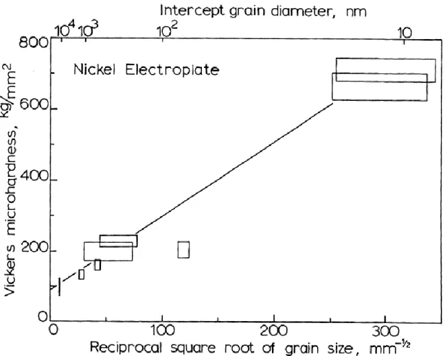
Thus, by decreasing the grain size, significant gains in strength and hardness can be obtained. A
hardness against grain size plot for electrodeposited nickel is shown in Fig. 2.8. The effect of
grain size on hardness and strength can be understood when considering that grain boundaries
and triple junctions are barriers to hinder dislocation motion in materials [Hall (1951), Petch
(1953), Wang et al. (1995)]. With the reduction in grain size the volume fraction of the
intercrystalline component increases, thus there is a greater number of barriers resulting from
18
Figure 2.8: Plot of Vickers micro-hardness against one over square root of grain size, [Huges et al. (1896)]
2.4 Deformation Mechanisms in Nanocrystalline Materials
The primary deformation mechanisms for polycrystalline materials at low temperature are
dislocation slip and twinning. To activate other mechanisms such as grain boundary sliding,
grain rotation and diffusional mechanisms, higher temperatures and/or high stresses are required.
In nanocrystalline materials, the volume fraction of intercrystalline defects is significantly higher
than in polycrystalline structures. With the larger volume fraction of grain boundaries and triple
19
movement or twinning. Many previous studies have shown that plastic deformation in
nanocrystalline materials at ambient temperature could be accommodated by diffusional creep,
grain boundary sliding and grain rotation [e.g. Whang, (2011)], such as summarized in Fig. 2.9.
Figure 2.9: Low temperature deformation mechanisms in nanocrystalline metals, from [Erb et al. (2004)]
2.4.1 Grain Boundary Sliding and Grain Rotation
Grain boundary sliding is a macroscopic deformation mechanism where un-deformed grains
slide over each other along their common boundaries. The original theory for polycrystals was
presented by Gifkins and Snowden [1966] and later further developed by Ashby and Verall
[1973]. This process is accommodated with other deformation mechanisms such as grain
rotation and diffusional processes.
50 nm
b20
Gifkins and Snowden proposed that grain boundary sliding is induced by applied stress, where
the adjacent grains slide in the opposite directions and the protrusions within the boundary move
through lattice diffusion. Thus, protrusions within the grain boundaries hinder the rate of grain
boundary sliding. As seen in Fig. 2.10a, under the applied stress, the top grain slides to the right
and the bottom grain slides to the left. The rate of boundary sliding is reduced due to the
movement of the protrusion, YX. As the grains slide over one another, the protrusion is under
a) b)
Figure 2.10: Schematic diagram of a) grain boundary sliding with a protrusion in the boundary, b) grain boundary sliding of the triple junction, Gifkins and Snowden [1966]
compressive stress at X and tensile stress at Y. The tension region has a higher concentration of
vacancies than the compression region X. Thus, the tension region acts as a vacancy sink and
the atoms in the compression region diffuse to the other side, thereby moving the protrusion
towards the right.
In 1968, Gifkins further developed the model and proposed that the rate determining step of
21
grain number 1 moves to the right while grain number 2 moves to the left. This creates a
compression stress on the BC boundary and a tensile stress on the BD boundary. Since boundary
BD has a higher vacancy concentration than boundary BC, the atoms in BC diffuse to boundary
BC, whereby boundary BC will slide to the right and boundary BD will slide to the left.
Ashby and Verral [1973] and Hahn et al. [1997] have proposed alternative models where grain
boundary sliding is accommodated with diffusional mechanisms in polycrystalline and
nanocrystalline materials, respectively. In Ashby and Verral's model, it is suggested that as one
grain slides over another grain in polycrystalline materials, the local deformation on the adjacent
boundaries accommodates changes through Coble and/or Nabarro-Herring creep. This allows
the grains to remain wedged together and the rate determining step for this model is suggested to
be the diffusion mechanisms, Coble and Nabarro-Herring creep.
22
The model developed by Hahn et al. [1997] is explicitly for grain boundary sliding in
nanocrystalline materials, Fig. 2.11. By assuming all grains in a material have similar shape and
size, Hahn et al. proposed that there's a macroscopic sliding plane (denoted by the black area
between the parallel lines) between the non-deforming grains (denoted by the white area), in
which these planes are activated to accommodate the deformation. Prior to sliding, deformation
is accommodated through grain boundary diffusion (Coble creep) along the interfaces. The
sharp edge of each grain is smoothened by diffusion to form the sliding plane. Grain boundary
sliding can only occur after the applied stress overcomes a certain threshold value. Molecular
dynamics simulations on sliding along grain boundaries were carried out by van Swygenhoven et
al. [2001]. Their results showed that grain boundary sliding is the primary deformation
mechanism in nanocrystalline materials. The sliding activity shown by the simulation is in
support of Hahn's model where grain boundary sliding is facilitated by stress assisted atomic
diffusion.
During grain boundary sliding, grain rotation can also occur simultaneously in which the grains
turn in the direction of the shear stress [e.g. Murayama et al. (2006)]. The adjacent grains may
rotate to a point where their orientations are closer to each other, which leads to softening.
Murayama et al. suggested that grains can rotate by disclination motion, where a disclination is a
line defect characterized by a rotation of the crystalline lattice around its line [Klimanek et al.
(2001)] and the motion of disclination dipole is a combination of two disclinations which causes
23
Figure 2.12: Schematic diagram of grain rotation of nanocrystalline material under tensile loading due to disclination dipole motion, as proposed by Ovid'ko [2002]
2.4.2 Nabarro-Herring Creep
Diffusion mechanisms for the deformation of polycrystalline materials were proposed by
Nabarro [1948] and further developed by Herring [1950]. Self-diffusion within the grains of a
polycrystalline material is driven by the applied shear stress. Vacancies within a grain can be
created under compression or tension and they can move through grain boundaries or lattice
diffusion. In the presence of tensile stress on a grain boundary, the energy needed for vacancy
formation is reduced by the atomic volume multiplied by the applied stressed normal to the
boundary. On the other hand, when a grain boundary experiences a compressive stress, the
energy required for vacancy formation is increased by the same amount. Thus, the formation of
vacancies at a grain boundary is more preferable under tensile stress than compressive stress and
the annihilation of vacancies is the opposite. Diffusion of matter within the grain flows towards
the vacancies, from the compression region towards the area under tension. Thus, in the
presence of stress, there is a pressure gradient within the lattice and lattice defects such as
24
concentration of vacancies varies across the grain based on its shape and these vacancies move
through the grain by lattice diffusion. Fig. 2.13 is a schematic diagram of a polycrystalline solid
showing the macroscopic stress state. The directional flow of vacancies is shown by the arrows.
Atoms and vacancies diffuse through the crystalline lattice to the grain boundaries, resulting in
macroscopic deformation.
Figure 2.13: Nabarro-Herring vacancy diffusion mechanism through a grain during loading, Herring [1949]
2.4.3 Coble Creep
Another deformation mechanism through diffusion was proposed by Coble [1963]. Similar to
Nabarro-Herring creep, Coble creep is a diffusion process that is induced by stress; however, the
diffusion of vacancies/atoms occurs through grain boundaries instead of the crystal lattice.
Coble proposed that the absorption and generation of vacancies is uniform along a given grain
boundary; however, the various angles of planar grain boundaries with respect to the applied
25
the opposing stress, σn, a vacancy concentration gradient arises between the boundaries. As shown in Fig. 2.14, two boundaries are under compressive stress while the other two boundaries
are in tension; this leads to the diffusion of vacancies toward the boundaries under compressive
stress and diffusion of atoms toward boundaries under tensile stress. Thus, the diffusive current
is similar to Nabarro-Herring's model. As mentioned above, with the reduction in grain size to
the nanocrystalline regime, the volume fraction of grain boundaries and triple junctions increases
by a significant amount. Hence, it is likely that Coble creep becomes the dominant deformation
mechanism as grain size decreases.
Figure 2.14: Coble vacancy diffusion mechanism along grain boundary during loading, Ashby [1969]
2.5 Strain Hardening in Polycrystalline and Nanocrystalline
Materials
Strain hardening of polycrystalline materials is a result of the increase in dislocation interactions.
Plastic deformation of polycrystalline materials can be separated into stages; in the early stage,
there is a random distribution of few dislocations in the crystal structure. These dislocations can
move along their slip planes with minimum interference from other dislocations. As plastic
26
results in a decrease in mean free dislocation length [Kuhlmann-Wilsdorf (1989)]. With further
deformation, the dislocation density increases even more and dislocations begin to pile up at
strong obstacles such as grain boundaries; this impedes dislocation motion on their respective
Fig. 2.15: The strain hardening behaviour of copper, brass and steel increase in tensile strength with increase in cold work [Callister (2005)].
slip plane. Thus, the mobility of a dislocation is reduced and higher stress is required for further
deformation. Most polycrystalline metals strain harden at room temperature. For example, Fig.
2.15 shows that the tensile strengths of copper, brass and 1040 steel increase significantly with
27
A previous study done by Liang and Yu demonstrated the strain hardening affect in
polycrystalline nickel [Liang and Yu (2008)]. Liang and Yu introduced strain into the material
through cold rolling. The specimens were cold rolled in small increments and water quenching
was used after each pass. The specimens were rolled to a strain of 80%, where strain, ε, was
given as
(6)
where Lf and Lo are the final and initial lengths of the specimens. Vickers micro-hardness was measured for fully annealed Ni and at strains of ~10, 20, 40, 60 and 80%, respectively. The
hardness value increased twofold from 1 GPa to over 2 GPa at 80% elongation, Fig. 2.16. The
material had the highest strain hardening, between 0-20% elongation. With further deformation
to 80% elongation, the strain hardening rate was reduced.
Figure 2.16: Plot of Vickers micro-hardness against elongation for as-received and cold-rolled polycrystalline nickel [Liang and Yu, (2008)]
Elongation (%) 0 20 40 60 80 100 M icro ha rdnes s ( G P a ) 0 1 2 3 4 5 6 Nanocrystalline Ni
28
Since strain hardening is due to dislocation-dislocation interactions, in order to form a
dislocation pile-up against grain boundaries, at least two dislocations are needed [Callister
(2005)]. Nieh and Wadsworth proposed that dislocation pile-ups can only be generated within a
grain that is over a critical size [Nieh and Wadsworth, (1991)]. When grains are below the size
where two dislocations cannot co-exist within the same slip plane within one grain, dislocation
mechanisms may not be suitable to interpret the deformation behavior. Eshelby’s analysis of the
critical distance between two dislocations provides an estimate of the lower and upper limits of
grain size for dislocations to form a pile-up within a grain [Eshelby et al. (1951)]. The critical
distance, dc, between two dislocations is given by,
(7)
where τc is the critical shear strength, b is the Burgers vector of the dislocation and K is the energy factor. Since the variables K and b are material constants, the distance between two
dislocations is determined by the shear strength. To estimate the lower limit of grain size,
theoretical shear strength, , which is the highest shear stress the material can with-stand, is
used. The upper limit is estimated by using the Peierls-Nabarro force, , the lowest shear
stress required to move a single dislocation. Peierls-Nabarro force is expressed as,
(8)
where G is the shear modulus, W is the width of the dislocation, b is the burger's vector and is
the Poisson's ratio. A previous study by Wang et al. [Wang et al. (1994)] has calculated the
critical distances for copper and nickel, given as (dc)u and (dc)L in Table 2.1. Thus, the smallest distance that two dislocations can be brought together without pushing them away in an infinite
crystal are 39.4nm and 25.6nm for the upper limits and 1.2 and 1.3 nm for the lower limits for
29
Table 2.1: Upper and lower limits for critical distance between two dislocations Crystal K (GPa) τmax
th
(GPa) τp-n (GPa) b (nm) (dc)U (nm) (dc)L (nm)
Cu 78.2 1.54 1.91 0.286 39.4 1.2
Ni 126 3.71 3.71 0.275 25.6 1.3
Previous studies on the strain hardening capacity of nanocrystalline nickel were carried out by
Wang et al. [1994], Kulovits et al. [2008], Zabev [2008] and Wu et al. [2009]. In these studies,
different methods such as tensile deformation and rolling were used to introduce strain into the
specimens. In the studies by Zabev and Wu et al. samples of electrodeposited nanocrystalline
nickel were used. Plastic deformation was introduced into the specimens through cold rolling;
however, there is a considerable discrepancy between their results. Zabev obtained samples of
electroplated nanocrystalline from Integran Technologies, Inc. with a grain size of 29 nm. After
characterizing the as-received materials, the specimens went through cold-rolling in small
increments (1-5 µm thickness reduction per pass and water quenched after each pass). Zabev's
strain calculation were also based on the elongation of the sample in terms of length as given in
equation 6. Vickers micro-hardness was measured at different strains from 0% to 80%. It was
found that the hardness values fluctuated only slightly (Fig. 2.17), approximately by 7%, as
compared to polycrystalline nickel, which exceeded 100% in the initial stage, Fig. 2.16 and also
shown in Fig. 2.17 for comparison.
In contrast, Wu et al. [2009] reported significant yield strength increases for cryogenically
deformed nanocrystalline nickel electrodeposits with an initial grain size of 20 nm, Fig. 2.18.
Rolling strain was defined as
30
where ti and tf are the initial and final sample thickness, respectively. Fig. 2.18 is a plot of yield strength against rolling strain, which illustrates a sharp rise in yield strength, from 1400 MPa to
~2300 MPa, with increasing rolling strain to 0.5. For higher strains the yield strength decreased
to an intermediate value of ~1900 MPa.
Elongation (%) 0 20 40 60 80 100 M icro ha rdnes s ( G P a ) 0 1 2 3 4 5 6 Nanocrystalline Ni
Polycrystalline Ni [Liang and Yiu, 2008]
Figure 2.17: Plot of Vickers micro-hardness against elongation for as-received and cold rolled polycrystalline and nanocrystalline nickel [Zabev, (2008)]
The hardness against elongation plot obtained by Zabev, Fig. 2.17, led to the suggestion that the
strain hardening capacity of electroplated nanocrystalline nickel is low due to their inability to
accumulate dislocations. In contrast, strong strain hardening under large plastic deformation was
observed by Wu et al. In view of this discrepancy regarding strain hardening effects in nickel as
31
compare strain hardening in polycrystalline and nanocrystalline nickel based on hardness
indentations. This will be explained in more detail in section 4.3
Figure 2.18: Plot of yield strength against rolling strain, where yield strength is determined by one third of Vickers micro-hardness relationship [Wu et al. (2009)]
2.6 Hardness
Hardness is a mechanical property that is often used to for comparison between different
materials. The hardness of a material is defined as the material's resistance to localized
plastic/permanent deformation [Callister (2005)]. One group of tests used to determine hardness
are known as static indentation tests, where an indenter with the geometry of a ball, pyramid, or
diamond cone is pressed into the surface of the material being tested. The hardness is either
determined from the total test force to the penetration depth or the indentation area. Common
static indentation tests include Rockwell, Vickers, Brinell and Knoop hardness tests [Callister
32
2.6.1 Rockwell and Superficial Rockwell Hardness
Rockwell hardness is classified as a penetration method, Fig. 2.19. The principle of the test can
be divided into three steps: first, a minor load is applied to establish a reference point, and then a
major load is applied and held for a specified dwell time. Lastly the major load is removed and
the final depth of indentation is measured. The initial minor load eliminates the effects of
backlash in the measuring system and surface roughness which could lead to potential measuring
errors. There are two types of Rockwell hardness tests: Superficial Rockwell and Rockwell.
The difference between the two is the load selections for specimens with different thickness and
test locations. For Superficial Rockwell, the reference point is set by a minor load of 3kgf, and
major loads of 15, 30, or 45 kgf, respectively. On the other hand, the minor load in Rockwell
testing is 10kgf, and the major loads are 60, 100, or 150 kgf. The selection of indenter is
determined by the type of material to be tested and the scale limitations; for testing hard
materials the 120º sphero-conical diamond indenter is utilized to avoid plastic deformation of the
indenter during the test. Hardened steel ball indenters with diameter of , , , inches are used
for testing softer materials.
The hardness value is derived from the differences in the two indentation depth measurements, h
in mm, Fig. 2.19, where the Superficial Rockwell hardness value is given as,
(10)
On the other hand, the Rockwell hardness value is given as,
Ball indenter:
33 Diamond cone indenter:
(12)
Figure 2.19: Schematic diagram of the cross section of Rockwell hardness measurement, modified [ASTM E18 – 08, (2008)]
2.6.2 Brinell Hardness
Brinell hardness testing is another static hardness test which utilizes the indentation depth to
determine the hardness of materials. The test consists of applying a load between 500 to 3000
kgf for a specific dwelling time usually between 10 to 30 seconds using a hardened steel or
tungsten carbide ball with a diameter of 5 or 10 mm. Once plastic deformation is introduced into
the testing specimen, the resultant recovered round impression is measured in millimeters using a
low power microscope. Hardness is determined by taking the mean diameter of the indentation,
the hardness number (HB) is given as,
34
where P is the load in kg; D is the diameter of the indenter in mm; and d is the diameter of the
indentation in mm.
2.6.3 Vickers and Knoop Hardness
Vickers and Knoop micro-hardness are static indentation tests which utilize the area of the
indentation to provide the measure of hardness. The hardness test involves indenting a diamond
indenter of specific geometry into the surface of the test specimen at loads ranging from 1 to
1000 grams force. Both methods are used to determine the hardness of material geometries that
are too small to be measured by conventional macroscopic methods. The differences between
Vickers and Knoop hardness test is the geometry of the indenter, Fig. 2.20. The Vickers indenter is a square based pyramidal diamond with a face angle of 136, while the Knoop indenter is a rhombic based pyramidal diamond shape. The long to short diagonal ratio for the Knoop indenter is about 7 to 1 with a longitudinal angle of 172 and a 130 transverse angle. With the difference in indenter geometry, Vickers indenter penetrates into the specimen about
twice as far as compared to Knoop indenter; thus, the Vickers hardness test is less sensitive to
surface conditions than the Knoop test.
The hardness value for both Vickers and Knoop is a stress value with units of kilograms per
millimeter square. It is determined by the ratio of the applied load, P, to the unrecovered
projected area of indentation, A.
35
Figure 2.20: Schematic diagrams of the indenter and indentation of Vickers and Knoop hardness [Callister (2005)].
Vickers and Knoop hardness values are designated as HV and HK, respectively. The formula for
Vickers hardness (HV) is given as,
(15)
where P is the applied load in kgf; d is the mean diagonal of the indentation in mm;. The Knoop
hardness value (HK) is expressed as,
(16)
where P is the applied load in kgf; l is the measured length of the long diagonal in mm. Since the
width of the Knoop indenter is much thinner, it is often used to measure hardness on the
cross-sections of thin coatings.
2.6.4 Nanoindentation Hardness
Nanoindentation is a very popular technique used for studying the mechanical properties of
solids in submicrometer or nanometer size regions [e.g. Oliver et al. (1986)]. Similar to Vickers
36
indentation. The hardness test involves indenting the so-called Berkovich indenter into the
surface of the test specimen, Fig. 2.21.
Figure 2.21: Schematic diagram of the Berkovich indenter
Since the projected residual area of the indent is correlated with penetration depth, as the load is
applied the depth of penetration is measured and the area of contact is determined by the depth of
the impression and the known angle of the Berkovich indenter. The nanoindentation hardness
value is expressed as,
(17)
where H is the hardness value measured by nanoindentaiton, P is the applied load and hp is the measured displacement. With the smaller indentations, nanoindentation is often used to measure
mechanical properties of coatings and thin films.
2.6.5. Summary of Hardness Tests
For a quick comparison, the various hardness tests described in sections 2.6.1 - 2.6.4 are
summarized in the following table giving details on the indenter and the equations for the various
37
Table 2.2 Summaries of the static hardness indentation tests
Test Indenter Formula for Hardness Number
Rockwell and Superficial Rockwell Hardness
Diamond cone;
, , , in. steel spheres
Rockwell Hardness:
Superficial Rockwell Hardness:
Brinell 10 mm sphere of steel or
tungsten carbide
Where P is load, kg; D is sphere diameter, mm; d is diameter of the indentation, mm.
Vickers micro-hardness Vickers diamond pyramid
Where P is load, kgf; d is the mean diagonal of the indentation, mm
Knoop micro-hardness Knoop diamond pyramid
Where P is the applied load, kgf; l is the measured length of long diagonal, mm.
Nanoindentation hardness Berkovich diamond pyramid
Where P is the applied load, and hp is
the measured displacement of
penetration depth
2.7 Hardness Conversion Relationship
Hardness conversion tables for metals such as copper, steel and nickel can be found in ASTM
38
and Knoop hardness for different metals are generated empirically from the hardness numbers
contained in the tables. The hardness conversion tables for nickel and high-nickel alloys can be
found in the appendix. ASTM suggested that these hardness conversion tables and relationships
are intended for nickel and high-nickel alloys, where the nickel content is over 50 %, and
particularly for nickel-aluminum-silicon specimens. To cover the large range of hardness values,
these alloys were in their annealed to heavily cold-worked or age-hardening conditions,
including intermediate conditions. However, a Rockwell/Superficial Rockwell to Vickers
hardness conversion table and relationship has yet to be developed for polycrystalline and
nanocrystalline nickel in which strengthening is solely due to grain size refinement.
2.8 Objectives of this Research
As mentioned in the previous chapter, in industry hardness values are commonly reported in
terms of Rockwell hardness value. However, in the past most of the hardness measurements for
nanocrystalline metals were limited to Vickers micro-hardness and nano-indentation hardness
tests, mainly due to sample size/thickness limitations which did not permit the application of the
Rockwell method. Hardness conversion relationships for various hardness scales and materials
can be found in ASTM standards. For nickel the hardness relationship are based on the materials
in which the strengthening mechanism were through alloying, annealing, cold working, and age
hardening. However, there is no Vickers-Rockwell hardness conversion for polycrystalline and
nanocrystalline nickel, in which the strengthening mechanism is mainly due to grain size
refinement. The first objective of this thesis is to establish such a relationship for nickel
39
With respect to strain hardening of nanocrystalline nickel electrodeposits, there are conflicting
results reported in the literature. Some studies have concluded that strain hardening decreases
with decreasing grain size on the basis of tensile test results [Wang et al. (1997)], others studies
found very little to no strain hardening when strain was introduced through cold rolling [Kulovits
et al. (2008) and Zabev et al. (2008)]. In contrast, Wu et al reported significant strain hardening
capacity on the basis of relatively large yield strength increases for cryogenically deformed
nanocrystalline nickel. In view of these conflicting results regarding strain hardening effects in
nickel as a function of grain size, the second objective of this study was to use a different
experimental approach to compare strain hardening in polycrystalline and nanocrystalline nickel
40
3.0 Materials and Experimental Methods
The goal of this study is to investigate hardness scale conversions and the strain hardening
behaviour in localized deformation zones for nanocrystalline nickel. This section details the
procedures followed in sample preparation, materials characterization and the different types of
hardness measurements for polycrystalline and nanocrystalline nickel.
3.1 Materials and Sample Preparation
Eight specimens of nickel with different grain sizes and hardness were used to determine the
relationship between the Rockwell/Superficial Rockwell hardness scales and the Vickers
micro-hardness. The grain sizes of these specimens ranged from polycrystalline down to
nanocrystalline. The polycrystalline metal samples were commercially available Ni-200 samples
while the electrodeposited nanocrystalline nickels were provided by Integran Technologies Inc..
Several nanocrystalline samples contained some iron or phosphorus alloying additions.
However, from previous studies, it is known that the strengthening mechanism of these materials
comes mainly from grain size reduction and not solid solution hardening [Erb et al. (1996)]. For
Rockwell/Superficial Rockwell hardness testing, the samples were electroplated with thicknesses
between 0.6 mm to 1 mm in accordance with ASTM standard (E18-08) for Rockwell hardness
testing of materials.
To investigate the effect of grain size on strain hardening, four lots of nickel were selected, and
these materials were chosen from the two extreme ends of the grain size range. The work
41
inducted into the specimens through large Rockwell hardness indentations. An ASTM standard
Rockwell scale D, 120° diamond cone indenter at 100kgf of load, and a Rockwell scale B, ball
indenter at 100kgf of load, were used to introduce macro-indents on each specimen.
Subsequently, the specimens were sectioned near the Rockwell indentation followed by cold
mounting into epoxy. Grinding and polishing were used to expose the cross-section of the
indentation. To reduce residual stresses introduced during grinding and polishing, standard
LECO's metallographic polishing procedures using progressively finer polishing media were
utilized. To determine the changes in hardness due to the localized deformation in the plastic
zone, hardness profiles along direction, x, away from the Rockwell indentation were measured
using a much smaller Vickers micro-hardness indentations, Fig. 3.1. For higher resolution of
hardness closer to the Rockwell indent, nano-indentation hardness contours were also carried out
for the smallest grained nickel. Similar to Vickers micro-hardness, the sample surface
preparation was as per ASTM standard (E2546-07) for nano-indentation.
Figure 3.1 Schematic diagram of the cross sections below the Rockwell indentations. Vickers micro-hardness profiles were measured along direction x.
42
3.2 Material Characterization
3.2.1 Energy-Dispersive X-ray Spectroscopy (EDX)
The compositions of the materials were determined by energy-dispersive X-ray spectroscopy
(EDX) in a conventional Hitachi S-570 field emission scanning electron microscope (SEM), at
an acceleration voltage of 20 kV. The specimens were prepared by wet-grinding and a total of
three measurements were made on each specimen using the area mode to analyze large areas
(~100 x 100 µm) on the specimens.
3.2.2 Grain Size Analysis
3.2.2.1 Transmission Electron Microscopy (TEM)
To investigate the microstructures and grain sizes of the nanocrystalline specimens, bright field
and dark field images and selected area diffraction patterns (SADP) were required. For this
analysis, a Philips CM12- LaB6 TEM, with an operating accelerating voltage of 200kV was utilized. To prepare the TEM specimens, the bulk materials were mechanically ground and
polished down to a thickness of approximately 100 µm. Subsequently, 3 mm discs were
mechanically punched out (Gatan sample punch) for further preparation. To create the thin
electron transparent area, the 3 mm discs were electropolished using a Struers TenuPol-5 twin-jet
electropolisher. The electrolyte used consisted of 90% methanol and 10% perchloric acid and
the temperature was kept between -40ºC to -50ºC with liquid nitrogen cooling. The polishing
was achieved at a voltage of 15V, at 74-95mA current density for 1 minute and 15 seconds per
disk. The average grain sizes were calculated from grain measurements on dark field images
![Figure 2.1: (a) Schematic representation of ECAP [Komura et al. (1999)], (b) the four processing routes for ECAP with sample rotation between each pass [Iwahashi et al](https://thumb-us.123doks.com/thumbv2/123dok_us/10009374.2899151/17.918.216.716.243.996/figure-schematic-representation-komura-processing-routes-rotation-iwahashi.webp)

![Figure 2.4: Schematic diagram of an electrodeposition set up [Cheung (2001)]](https://thumb-us.123doks.com/thumbv2/123dok_us/10009374.2899151/22.918.169.752.277.716/figure-schematic-diagram-electrodeposition-set-cheung.webp)

![Figure 2.11: Schematic diagram of grain boundary sliding, proposed by Hahn et al. [1997]](https://thumb-us.123doks.com/thumbv2/123dok_us/10009374.2899151/31.918.269.656.645.1018/figure-schematic-diagram-grain-boundary-sliding-proposed-hahn.webp)
![Figure 2.12: Schematic diagram of grain rotation of nanocrystalline material under tensile loading due to disclination dipole motion, as proposed by Ovid'ko [2002]](https://thumb-us.123doks.com/thumbv2/123dok_us/10009374.2899151/33.918.193.725.115.359/figure-schematic-diagram-rotation-nanocrystalline-material-disclination-proposed.webp)
![Figure 2.13: Nabarro-Herring vacancy diffusion mechanism through a grain during loading, Herring [1949]](https://thumb-us.123doks.com/thumbv2/123dok_us/10009374.2899151/34.918.246.689.315.678/figure-nabarro-herring-vacancy-diffusion-mechanism-loading-herring.webp)
![Fig. 2.15: The strain hardening behaviour of copper, brass and steel increase in tensile strength with increase in cold work [Callister (2005)]](https://thumb-us.123doks.com/thumbv2/123dok_us/10009374.2899151/36.918.254.670.231.698/strain-hardening-behaviour-increase-tensile-strength-increase-callister.webp)
![Figure 2.17: Plot of Vickers micro-hardness against elongation for as-received and cold rolled polycrystalline and nanocrystalline nickel [Zabev, (2008)]](https://thumb-us.123doks.com/thumbv2/123dok_us/10009374.2899151/40.918.207.709.322.676/figure-vickers-hardness-elongation-received-rolled-polycrystalline-nanocrystalline.webp)
