Fabrication of ferroelectric based
MEMS structures for electronically
s
witchable b
ulk
a
coustic
w
ave
r
esonator
s
By Tian Le Wang
This thesis is submitted to Materials Department,
Imperial College London for the degree of Doctor
Of Philosophy
Feburary 2
014
Abstract
The thesis describes the research carried out into fabrication of multilayer microwave capacitance structure with ferroelectric films in paraelectric state; and confirmation of the possibility to develop on their base an electronically switchable bulk acoustic wave (BAW) resonator. Different eigenmodes of acoustic resonances can be excited and switched electronically through the application to ferroelectric layers of the resonator unidirectional or oppositely directed dc biased electric fields..
The resonator was fabricated out of a SrRuO3/SrTiO3/SrRuO3/YSZ multilayer structure deposited on top of Si substrate. Pulsed Laser Deposition, Magnetron Sputtering, Photolithography, Argon Ion Beam Milling, and Reactive Ion Etching were the fabrication methods used to make this resonator.
This novel device is a demonstrator that will contribute to the telecommunications industry’s demand for flexibility in both microwave frequency switching and tuning. The Si MEMS concept of this resonator allows easy circuit board integration into many electronics products.
Preface
This thesis is the author’s own work and is submitted for the degree of Doctor of Philosophy at Imperial College London.
Parts of this thesis have either been published, presented at conferences,accepted for publication or are in the preparation for submission.
T.Wang; P.K.Petrov; N.M.Alford; A.K.Mikhaylov; S.V.Ptashnik; S.V.Zinoviev and
A.B.Kozyrev, Electronically switchable bulk acoustic wave resonator based on
paraelectric state ferroelectric films. Electronics Letters, 2011. 47(24)
T.Wang; P.K. Petrov and N.M. Alford, Deep reactive ion etching of silicon for MEMS
applications, Poster Presenation at VS3 Nanostructured Metal Oxide Thin Films, Coventry, UK 2012
T.Wang; P.K. Petrov and N.M. Alford, Alternative deep reactive ion etching of
silicon using metal masks. MRS Conference 2012 Symposium DD, Boston, USA P.K.Petrov;T.Wang;N.M.Alford A.K.Mikhaylov; S.V.Ptashnik; S.V.Zinoviev and
A.B.Kozyrev, Free-standing nanoscale functional oxides multlilayer structure for
electronically switchable bulk acoustic wave resonators. EMRS Conference 2013 Symposium H, Strasbourg, France
T.Wang; P.K.Petrov and N.M.Alford, Alternative deep reactive ion etching of silicon
using metal masks. Journal of Micromechanics and Microengineering, 2014
The copyright of this thesis rests with the author and is made available under a Creative Commons Attribution Non-Commrcial No Derivative license. Researchers are free to copy, distribute or transmit the thesis on the condition that they attribute it, that they do not use it for commercial purposes and that they do not alter, transform or build upon it. For any reuse or redistribution, researchers must make clear to others the license terms of this work.
Table of Contents Page
Abstract ... 2 Preface ... 3 Figure Contents ... 6 Table Contents ... 10 Acronyms ... 12 Acknowledgements ... 14 Chapter 1. Introduction ... 15
1.1 Introduction and Motivation ... 15
1.2 Thesis Facts Known and Unknown ... 17
1.3 Thesis Overview ... 17
1.4 Original Contributions ... 18
Chapter 2. Literature Review ... 19
2.1 Basic Ferroelectric Properties ... 19
2.2 Bulk Acoustic Wave Resonator ... 32
2.2.1 State of Art of Ferroelectric Materials in BAW Resonators ... 35
2.2.3 Types of Bulk Acoustic Wave Resonators ... 42
2.2.4 BAW Device Performance Requirements ... 45
2.3 Dielectric Acoustic Wave Resonator ... 49
2.4 Fabrication Technologies ... 54
2.4.1 Magnetron Sputtering ... 54
2.4.2 Pulsed Laser Deposition ... 56
2.4.3 Silicon Substrate Patterning ... 58
2.4.4 Device Patterning ... 61
2.5 Characterisation Techniques ... 65
2.5.1 Optical Microscopy ... 65
2.5.2 Scanning Electron Microscopy ... 66
2.5.3 X-Ray Diffraction ... 68
2.5.4 Profilometry ... 70
2.5.5 Electrical Characterisation ... 72
2.6 Conclusion ... 84
Chapter 3. Deposition and Characterisation of Thin Film Multilayer Structure ... 85
3.1 Processing Overview ... 85
3.2 Deposition of 8 mol% Yttria Stablized Zirconia(YSZ) buffer layer by Pulsed Laser Deposition ... 87
3.3.1 Deposition of Strontium Ruthenate (SrRuO3) Electrodes by Pulsed Laser Deposition ... 89
3.4.1 Deposition of Strontium Titanate (SrTiO3) Active Layer by Pulsed Laser
Deposition ... 94
3.4.2 Tunability vs. Frequency Measurement Results ... 98
3.5 Metal Layer Deposition ... 100
3.6 Conclusions ... 101
Chapter 4. Deep reactive ion etching of Silicon ... 102
4.1 Optimisation of the Si reactive ion etching process ... 102
4.2 Choice of the masking material for Si reactive ion etching ... 109
4.3 Conclusions ... 115
Chapter 5. Fabrication of a ferroelectric based tunable thin-‐film bulk acoustic wave resonator ... 116
5.1 Device Design ... 116
5.2 Device Mask Design ... 117
5.3 Resonator Patterning ... 119
5.3 Resonator device measurement results ... 123
5.4 Conclusions ... 127
Chapter 6. Theory and Device Operation ... 128
6.1 Theory and Device Operation of One Stacking Structure ... 128
6.1.1 Introduction ... 128
6.1.2 Theory of field dependent acoustic resonances ... 129
6.1.3 Theory of field dependent piezoelectric constitutive equations ... 132
6.1.4 Series and Parallel Resonance ... 133
6.2 Device Operation of Two Stacking Structure ... 135
6.3 Conclusion ... 136
Chapter 7. Conclusion and Future Works ... 137
References ... 138
Appendix I. ... 145
Modeling of the Resonator Device ... 145
Figure Contents
Figure 2.1.The crystallography structure of ABO3 type material an the unit cell
response to external electric field...20
Figure 2.2.The classification of the ferroelectric materials from the general class of dielectrics...21
Figure 2.3.Temperature dependence of the relative dielectric constant of a ferroelectric material and different responses to electric field in ferroelectric and paraelectric states...22
Figure 2.4.Temperature dependence of the loss tangent at zero biasing field for single crystal Strontium titanate at microwave frequencies...23
Figure 2.5.Variation of dielectric constant and loss factor with frequency of an AC electric field...26
Figure 2.6.The model of the interfacial dead layer within a ferroelectric device and the dependence of dielectric properties on the thickness of BST50/50 thin films...28
Figure 2.7.The bias induced resonant dips observed in BST50-50 based capacitors from 0V-20V...30
Figure 2.8.Electrical input impedance of a BAW resonator...35
Figure 2.9 The DC bias dependence of a resonant frequency and reflected power corresponding to states (on and off) at T=52K and DC field of 1.2kV/cm...40
Figure 2.10.The relationship between Curie temperature and Ba concentration for BST ceramic and single crystals and Temperature dependence of dielectric constant of BST ceramic for different Ba concentrations...41
Figure 2.11.Thin film acoustic resonator setup and Solidly mounted resonator topology...43
Figure 2.12.Thickness mode and Contour mode acoustic wave resonators...45
Figure 2.13.Excitation of wavefronts inside a resonant cavity...46
Figure 2.14.Potential applications of ferroelectric materials...53
Figure 2.15.Commercial applications relating to SAW, BAW and Temperature Compensated SAW technologies...53
Figure 2.16. Difference between the DC and RF magnetron sputtering system and the schematic of the magnetron sputtering system...55
Figure 2.17.Electrical resistivity vs. Argon pressure for sputtered titanium films and Zone model showing the influence of argon pressure and substrate temperature on the microstructure of metal thin films...56
Figure 2.18.The instrument setup of a pulsed laser deposition system...57
Figure 2.19.Growth temperature Td, thickness t and lattice parameters a of the multilayer structure...58
Figure 2.20. Difference between the wet etching and dry etching techniques...58
Figure 2.21. The system schematic of reactive ion etcher and inductively coupled plasma etcher...60
Figure 2.22. Results of deep silicon etching from different etching processing conditions...61
Figure 2.23.Contact, proximity and projection alignment systems...62
Figure 2.24. Ion beam milling system schematic...63
Figure 2.25. The etching rate of different materials vs. the angle of incidence during ion beam milling...64
Figure 2.26.Ion beam etching rate of different materials and Kaufman type ion beam etching system...64
Figure 2.27. The schematic of transmission and reflection optical microscope...65
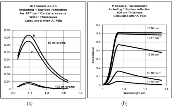
Figure 2.28. Si transmission improves with wafer thinning and P-type doped Si transmission decreases with increasing carrier concentration...66
Figure 2.29.Schematic diagram of a scanning electron microscope...68
Figure 2.30. XRD diffraction pattern for STO and BST films grown at 400 °C and 500°C...69
Figure 2.31. An X-ray beam scan process and relationship to Bragg’s Law...69
Figure 2.32. The schematic setup of a contact stylus profilometer...71
Figure 2.33.Different types of ferroelectric capacitors...73
Figure 2.34. Coplanar transmission line structures patterned on ferroelectric film...74
Figure 2.35. Frequency range applicability for each measurement techniques and the associated instrumental error/limits...75
Figure 2.36. Setup for current voltage measurement...76
Figure 2.37. Four point probe method of measuring resistivity of a specimen and the electrical field and equipotential line distribution on the sample during four point probe technique...77
Figure 2.38. Different measurement techniques used for different frequency ranges...78
Figure 2.39.The different measurement configurations for different impedance samples...79 Figure 2.40. Simplified diagram of the RF I-V technique setup...80 Figure 2.41. The two types of capacitance measurement circuit modes-Parallel and Series Equivalent mode...80 Figure 2.42. Setup for capacitance voltage measurement and the calibration
standards for measurements...81 Figure 2.43. Circuit model used to characterized the resonator performance...81 Figure 2.44. The Open/Short/Load compensation for RF IV measurement...82 Figure 2.45. One port measurement setup for resonator device characterisation....83 Figure 2.46. The calibration standard values for network analyzer in Vector
impedance plane and Smith Chart...84 Figure 3.1. The fabrication process of the bulk acoustic wave resonator...85 Figure 3.2. Crystal structure of Yttria Stabilized Zirconia...88 Figure 3.3. X-ray 2θ diffraction pattern of YSZ on Si substrate with native oxide and Si substrate with HF etching treatment...89 Figure 3.4. The orthorhombic crystal structure of SrRuO3 with lattice
parameters...91 Figure 3.5. Schematic drawing of the rectangle on cube epitaxial relation of SRO on YSZ...91 Figure 3.6. X-ray 2θ diffraction pattern of SRO on Si substrate...93 Figure 3.7. X-ray 2θ diffraction pattern of SRO on YSZ buffered Si substrate...93 Figure 3.8. The current voltage curve for the bottom electrode deposited directed on silicon substrate and deposited on YSZ buffered silicon substrate...94 Figure 3.9. X-ray 2θ diffraction pattern of STO thin films grown on SRO electrodes on Si substrate at different substrate temperature and at a constant oxygen partial pressure...96 Figure 3.10. X-ray 2θ diffraction pattern of STO thin films grown on SRO electrodes on Si substrate at different oxygen partial pressure and at a constant substrate temperature and an enlarged comparison XRD graph at STO (110) peak...97 Figure 3.11. X-ray 2θ diffraction pattern of STO thin films grown on SRO electrodes on YSZ buffered Si substrate at 850°C and 150mTorr O2 partial pressure...98 Figure 3.12. The capacitance-voltage behaviour of the resonator device at various frequencies with applied voltage from-2V to 2V...99
Figure 3.13. Frequency vs. Tunability of the 300nm SRO/500nm STO /300nm
SRO/10nm YSZ on Si multilayer structure ...99
Figure 4.1. Etch rates of Silicon vs Pressure under CF4 plasma...103
Figure 4.2. Etch rates of Silicon vs Pressure under Argon plasma...103
Figure 4.3. Etch rates of Silicon vs Pressure under CF4(25%)+Ar(75%) plasma mixture...104
Figure 4.4. Etch rates of Silicon vs Pressure under CF4(50%)+Ar(50%) plasma mixture...104
Figure 4.5. Etch rates of Silicon vs Pressure under CF4(75%)+Ar(25%) plasma mixture...105
Figure 4.6. Etch rates of Silicon vs Pressure under CF4 at 100V RF bias...106
Figure 4.7 Etch rates of Silicon vs Addition of Oxygen in CF4(25%)+Ar(75%) plasma mixture at 60Pa ...108
Figure 4.8 Etch rates of Silicon vs Addition of Oxygen in CF4(75%)+Ar(25%) plasma mixture at 60Pa ...108
Figure 4.9 Etch rates of Silicon vs Pressure in CF4(40sccm)+Ar(10sccm)+O2(5sccm) plasma mixture at 100V RF bias ...109
Figure 4.10. The chemical and physical reactions occurring during the etching process...110
Figure 4.11. The mask fabrication processing route...110
Figure 4.12. The relationship between Electronegativity and the silicon etching rate...112
Figure 4.13. The SEM images of Si etching profiles using different masking multilayer structures...113
Figure 4.14. X-ray diffraction pattern of the multilayer structure before and after the backside etching process...114
Figure 5.1. Bulk acoustic wave resonator configuration...116
Figure 5.2. Microscopic image of the bottom electrode pattern...117
Figure 5.3. Microscopic image of the ferroelectric layer pattern...118
Figure 5.4. Microscopic image of the top electrode pattern...118
Figure 5.5. Microscopic image of the substrate backside etching pattern...119
Figure 5.6. Microscopic image of the bottom electrode layer patterning on the SRO+YSZ layer...120
Figure 5.7. Microscopic image of the active layer patterning on the STO+SRO+YSZ layer...120 Figure 5.8. Microscopic image of the top electrode layer patterning on the
SRO+STO+SRO+YSZ layer ...121 Figure 5.9. Microscopic image of the silicon substrate backside patterning on the silicon substrate...122 Figure 5.10. Microscopic image of the three different active area dimensions and final device structure 50×50µm after photolithography patterning and ion beam milling steps...123 Figure 5.11. The capacitance voltage and current voltage measurement at different frequencies for the entire resonator device after silicon substrate backside
etching...124 Figure 5.12. The capacitance frequency measurement from the one port reflection setup compared with modelling...125 Figure 5.13. Results of phonon transport theory...126 Figure 6.1. Layout of the one stacking structure for FBAR resonator...129 Figure 6.2. Simplified cross section (a) and two terminal equivalent circuit of a tunable FBAR as a frequency selective switch...130 Figure 6.3. The series resonant circuit diagram and the parallel resonant circuit diagram...134 Figure 6.4. The series frequency response and the parallel frequency
response...134 Figure 6.5. Layout of the two stacking structure for the electronically switchable FBAR resonator...136
Table Contents
Table 2.1.Comparison between the ferroelectric materials and piezoelectric materials
in terms of mechanical and electrical properties...32
Table 2.2.Summary of dielectric properties measurements reported for STO and BST thin films...36
Table 2.3.Summary of various ferroelectric materials based tunable FBARs...38
Table 2.4.Comparison of different technologies for microwave devices...52
Table 2.5.Typical Specifications of a Stylus Profiler...72
Table 3.1. Growth conditions for each layer within the multilayer structure for the bulk acoustic wave resonator...86
Table 3.2. Physical properties of the materials used in the pulsed laser deposition...92
Table 3.3. The sputtering conditions for different metal mask materials...100
Table 4.1. The etch rates of Si and different masking materials...111
Table 4.2. The etching rates of different multilayer masking structures against the reactive plasma...113
Acronyms
AC
Alternating Current
BAW
Bulk Acoustic Wave
BSE
Backscattered Electrons
BST
Barium Strontium Titanate
BTO
Barium Titanate
DC
Direct Current
DUT
Device Under Test
EHF
Extremely High Frequency
FBAR
Film Bulk Acoustic Wave Resonator
GPS
Global Positioning System
GSG
Ground Signal Ground
HRS
High Resistive Silicon
IC
Integrated Circuit
ICP
Inductively Coupled Plasma
LAO
Lanthanum Aluminate
MEMS
Micro-electro-mechanical Systems
NA
Numerical Aperture
PLD
Pulsed Laser Deposition
RF
Radio Frequency
RIE
Reactive Ion Etching
SAW
Surface Acoustic Wave
SDA
Semiconductor Device Analyzer
SE
Secondary Electrons
SEM
Scanning Electron Microscope
SHF
Super High Frequency
SMR
Solidly Mounted Resonator
SRO
Strontium Ruthenate
TFBAR
Thin Film Bulk Acoustic Wave Resonator
UHF
Ultra High Frequency
UMTS
Universal Mobile Telecommunications System
UV
Ultraviolet
WLAN
Wireless Local Area Network
XRD
X-ray Diffraction
Acknowledgements
I would like to thank my supervisor Professor Neil Alford for allowing
me to join his group to carry out this PhD project together with the
endless support and guidance towards me throughout this project.
I would like to especially thank my supervisor Dr.Peter Petrov for the
advice, encouragement and support regarding the experimental work of
this research project.
I would like to thank Professor Andrey Kozyrev for providing the
theorectical concept of this research. Without this, my PhD project would
have never occurred.
I would like to thank Dr. Bin Zou for the invaluable discussions and
tutoring relating to the fabrication and characterisation issues occurred
during this project.
I would like to express my thanks to Dr. Peter Gammon, Dr.Sean
McMitchell, Jing Pang, Evgeniy Donchev,Clementine Walker, Laurentiu
Braic. This work would not have been possible without the help and
support from all the students and staff in the Thin Film Technology Lab.
Finally I would like to sincerely thank my parents Jianxun Wang and
Suzhen Wang for their constant support and guidance. I would like to
thank my girlfriend Baoli He for her everlasting love and moral support
through the best and worst times of my PhD research at Imperial College
London.
Tianle Wang
London,UK
Januray 2014
Chapter 1. Introduction
This introductory chapter is to provide the overview of thesis and motivation for the work presented.
1.1 Introduction and Motivation
The evolution of wireless communication systems in recent years has been accelerating at an extraordinary pace. This is mainly due to the increasing public demand for greater functionality while demanding a reduction in size and cost. The modern smart phone of Apple Inc. known as the iPhone has been the revolutionary
product of the 21st Century and the competition in this market has only intensified
with time. This is where research in the reconfigurable technologies such as Multi-frequency band and multi-mode cellular networking, GPS and WLAN connectivity can expect to answer the questions posed by current and future demands. For example, most mobile phones nowadays operate on the third generation (3G) with higher data rate services for video calls, mobile internet access and mobile TV. These smart mobile phones with 3G capability are required to operate over the global UMTS frequency bands of 850/900/1700/1900/2100MHz and fulfil the GPS standards of 1.5GHz bands and WiFi in the 2.4/5.0GHz bands. With the newly developed successor- the fourth generation(4G) being gradually integrated into future wireless mobiles and computers, it is highly desirable to provide multi-frequency band and multi-mode wireless devices with increased data transfer speeds using a single hardware device. This also presents a difficult challenge to integrate this technology with elegant designs and cost effective materials for mass commercial production. Therefore by using a single electronically tunable device to replace several wireless transceivers will bring a massive cost savings.
The microwave resonator is based on the excitation of an electromagnetic wave and is a part of many devices such as filters, oscillators, amplifiers and frequency meters. The size of these devices is directly related to the wavelength of electromagnetic wave at a certain frequency, which is also related to the propagation velocity of the electromagnetic wave at the same time. The main goal of designing microwave devices are concentrated at achieving high performance with small size and integrated with different devices on one chipset. The resulting size of microwave resonators at RF/Microwave frequencies is a big limitation for integration of portable communication systems. The acoustic resonator is an elgant solution to these
limitations due to advantages like lower propagation velocity, smaller size and integrated circuits compatibility compared to the electromagnetic wave resonators. The unique property of the ferroelectric materials such as electric field dependent permittivity and relatively low loss at microwave frequencies have made them promising candidates for electrically tunable RF and microwave devices in the wireless communication application. Ferroelectric materials are widely used in tunable microwave components such as tunable resonators, variable capacitors, phase shifters and filters.
This thesis proposes to use ferroelectric thin films for novel switchable and tunable bulk acoustic wave resonators at RF and microwave frequencies. The main focus of this thesis is to fabricate a novel type of thin film bulk acoustic wave resonator(TFBAR) on Si substrate using a MEMs setup and characterisation of ferroelectric thin films at microwave frequencies. The free standing TFBAR resonator will consist of single multilayer structure consisting of SrRuO3/SrTiO3/SrRuO3/YSZ deposited on the silicon substrate. The multilayer structure will be grown by PLD technique and an air cavity will be etched through the substrate using metal mask assisted dry etching method to create the free standing structure. The switchable and tunable characteristics of this resonator are based on the field dependent behaviour of the ferroelectric material in paraelectric state under DC bias. In current switchable and tunable microwave devices, external switches and varactors are required for frequency tuning, which results in increased loss in the path of RF signal, circuit design complexity and cost. Thus, by successfully fabricating prototypes of these intrinsically tunable resonators, we can contribute to the design and production of energy saving, cost effect and compact microwave systems. The principle of operation has been theoretically demonstrated recently by our colleagues from Professor Andrey Kozyrev’s group from St.Petersburg State Electrotechnical
University (LETI).[1]
The thesis presents the fabrication of the SrRuO3/SrTiO3/SrRuO3/YSZ multilayer structure on the silicon substrate, the development of a new alternative etching method for the silicon substrate and combining the deposition of the multilayer structure and the silicon etching technique to develop a novel TFBAR.
1.2 Thesis Facts Known and Unknown
Facts Known Facts Unknown
Pulsed Laser Deposition Conditions for SRO/STO/SRO/YSZ stack on Si substrate
How to make tunable BAW resonator in terms of deposition of multilayer stack?
Deep Reactive Ion Etching Conditions for fabricating free standing TFBARs on Si substrate
How to etch silicon substrate fast enough without ICP(Inductively Coupled Plasma)?
Masking Material Selection for etching through Si substrate
Which materials could be used as a resist?
Ferroelectric Material Selection for Tunable Bulk Acoustic Wave Resonator
How to protect the device side while maintain the functionality?
Design of the electrode structure for Tunable Bulk Acoustic Wave Resonator
Electrostriction are negative in terms of microwave losses, nobody utilized these materials for tunable BAW applications
1.3 Thesis Overview
The organization of the thesis is as follows.
Chapter 2 presents the background to concept of ferroelectricity, introduces the ferroelectric material system used for tunable microwave applications and reviews the fabrication and characterisation techniques involved in this project.
Chapter 3 details the fabrication and electrical characterisation of the YSZ/SRO/STO/SRO multilayer sturcutre on Si substrate. The influence of the PLD deposition conditions on the growth of epitaxial STO thin films has been studied. Chapter 4 describes an alternative Si deep etching method using metal masking materials developed to form a free standing MEMS structures. A Si etching rate of
11µm/min was achived using etching mixture of CF4(40sccm)+Ar(10sccm)
+O2(5sccm) at 60Pa pressure and 100V RF bias voltage and metal masking layers of 100nm Au/100nm Ti/100nm Au/100nm Ti.
Chapter 5 presents the design, the fabrication and the electrical performance measurement of an electronically switchable bulk acoustic wave resonators based on the ferroelectric MEMS structures.
Chapter 6 presents the theory of the single layer device as presented in the thesis and the desired two layer device. The device operation are explained qualitatively and final device layout is presented.
Chapter 7 concludes the thesis and outlines the directions for future work.
1.4 Original Contributions
This thesis has presented original contributions to knowledge of tunable ferroelectrics thin films for microwave applications. The summary of these contributions is listed below:
1. The processing conditions were established for epitaxial growth of
Strontium Titanate/Strontium Ruthenate multilayer thin films on high resistive Silicon substrate by pulsed laser deposition.
2. A novel alternative Silicon deep etching method using reactive ion milling
was established. This method demonstrates the possible incorporation in the device fabrication of the MEMs system.
3. A novel free standing functional oxides multilayer structure for
electronically switchable bulk acoustic wave resonator was proposed and fabricated on highly resistive Silicon substrate using pulsed laser deposition.
Chapter 2. Literature Review
This chapter gives an overview of the tunable microwave technologies and a general background introduction into the ferroelectric materials with detailed description of their dielectric, piezoelectric and acoustic properties. The current status and prospects are also reviewed. Various fabrication techniques are reviewed together with structural and electrical characterization to establish the relationship between processing parameters and material performance.
2.1 Basic Ferroelectric Properties
In 1921, Ferroelectricity was discovered by Joseph Valasek during an investigation of
the dielectric properties of the Rochelle Salt (NaKC4H4O6•4H2O) and demonstrated
the polarisation hysteresis with electric field and the temperature dependence.[2] Since
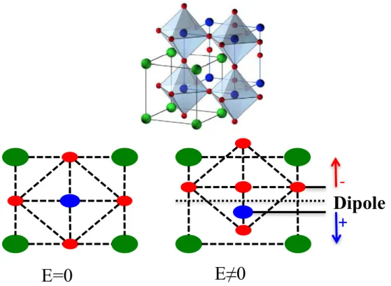
then the number of known ferroelectric materials has rapidly increased. Most of the useful ferroelectric materials belong to the perovskite family, which is characterised by the chemical formula ABO3. Figure 2.1 shows the cubic cell structure of the ABO3
type materials, with A2+ ions at the corner, B4+ions at the centre of the octahedral and
O2-ions at the face centres of the cube. This perovskite ABO3 structure allows variable
compositions by substituting on the A or B sites with compatible ions. When an
external electric field is applied, both B4+cation and O2-cation shift from their
equilibrium positions and form electric dipoles shown in Figure 2.1. This shift leads to the polarisation of the material under electric field and the shape of the unit cell is elastically deformed, which known as the Electrostriction effect. In contrast to the common converse piezoelectric effect, electrostriction is present in all dielectric materials and the deformation strain has a quadratic dependence on the magnitude of the applied electric field. Although the value of piezoelectricity induced by electrostriction effect may be small compared to the piezoelectricity in crystalline materials, they may be quite large in ferroelectric materials.
Figure 2.1. The crystallography structure of ABO3 type material and the unit cell response to external electric field (Green-A, Blue-B, Red-O)
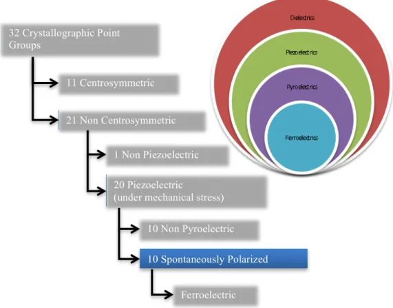
From the crystal symmetry, all of the crystal structures can be separated into 32 crystallographic point groups and only 11 of them are centrosymmetric. Centrosymmetric means the crystal contains a center of symmetry that inhibits any
polar properties from the crystal.[3] The other 21 crystallographic point groups are all
non-centrosymmetric and allow the crystal to contain one or more polar axes. All but one these non-centrosymmetric structure exhibit piezoelectricity described as a coupling between the electrical and mechanical energies. Piezoelectricity is linear with the applied electric field, so the piezoelectric response is reversed with the sign of the electric field is changed. 10 out of the 20 piezoelectric crystal point groups contains an unique polar axis and named as the polar crystals, because they posses a spontaneous polarization in absence of an external electric field. The spontaneous polarization is temperature dependent and its existence can be detected by observing the flow of charges to and from the surfaces on change of temperature. This known as the pyroelectric effect and the crystals with this effect are called pyroelectrics. A subgroup of the pyroelectrics is the ferroelectrics, which are polar materials that the direction of the spontaneous polarization can be switched by an external electric field. This classification is shown in Figure 2.2.
E=0
Dipole
-‐
+
E
≠
0
Figure 2.2. The classification of the ferroelectric materials from the general class of dielectrics
The piezoelectricity phenomenon was discovered in the 80s by the brothers Jacques
and Pierre Curie[4]. The direct piezoelectric effect is the ability to induce an electrical
polarization by the applied mechanical stress in crystals of certain categories. The converse piezoelectric effect is the production of a mechanical stress through the application of an electric field. The piezoelectricity phenomenon is reversible and expresses a linear interaction between mechanical and electrical domains in a single
elastic body. The relationship is mathematically correlated as below, [5]
S=s
ET+d
TE
(2.1)D=dT+ε
TE (2.2)where S is strain, s is compliance, T is stress, D is electric displacement, d is
piezoelectric coefficient,ε is permittivity, E is electric field strength.
Ferroelectric materials are a subset of the dielectric materials, which exhibit a reversible spontaneous polarization within a certain temperature range. The spontaneous polarization is temperature dependent and deceases with increasing temperature to disappear above a phase transition temperature known as the Curie
32 Crystallographic Point Groups 21 Non Centrosymmetric 11 Centrosymmetric 1 Non Piezoelectric 20 Piezoelectric
(under mechanical stress) 10 Non Pyroelectric 10 Spontaneously Polarized
point Tc. The ferroelectric material is in the paraelectric state when the temperature is above the Curie point Tc and exhibits a cubic structure. When the temperature is below Tc, the crystal structure experiences a slight deformation, the centre of positive charges and negative charges does not coincide, so the electric dipoles are formed and spontaneous polarisation occurs in the ferroelectric state. There is also a rapid decrease in the dielectric constant with further increasing the temperature after the
Curie point Tc and it follows the Curie-Weiss relationship.[6]
ε
!=
!!!!!
(T>T
c)
(2.3)where C is the Curie-Weiss constant, T0 is the Curie-Weiss temperature (normally below Tc, only equal to Tc for a continuous transition). The temperature effect on the dielectric constant and polarization and dielectric constant responses to applied electric field for ferroelectric phase transition to paraelectric phase are shown in Figure 2.3. Tunable ferroelectric based devices should operate slightly above their Curie temperature point in the paraelectric phase, because it retains a less dispersive permittivity at microwave frequencies and low hysteresis effect. In Figure 2.4, the microwave losses in single crystal strontium titanate is shown to be controlled not only by the bias field, but also sensitive to the temperature changes in the surrounding environment.
Figure 2.3.Temperature dependence of the relative dielectric constant of a ferroelectric material and different responses to electric field in ferroelectric and paraelectric states[7]
Figure 2.4. Temperature dependence of the loss tangent at zero biasing field for single crystal Strontium titanate at microwave frequeuncies [7]
Ferroelectrics can be divided into domains separated by domain walls, where domain is a group of unit cells within a single crystal and all of them has the same spontaneous polarization orientation. By applying alternating electric field, the spontaneous polarisation of domains will change repeatedly and this switching process results in a polarisation vs. electric field hysteresis loop. Generally, the existence of P-E loop is the evidence of classifying a ferroelectric material. In the paraelectric phase, the polarisation is strongly proportional to the external applied electric field and no hysteresis exists. In the ferroelectric phase, the polarisation does not go to zero when the external electric field is removed and exhibit a remanent polarisation Pr. This is due to the oriented domains being unable to return to their original random state without an additional energy input by an oppositely directed field, known as the coercive field Ec is needed to bring the polarisation to zero. Thus, the ferroelectrics operating at frequencies higher than 1MHz suffers from high dielectric losses. Further increasing the reverse electric field will lead to polarization saturation in the opposite direction.
The theory of ferroelectricity was first developed in 1949 by Devonshire and Landau[8,
9] to explain the ferroelectric phenomenon in BaTiO3. He used an expansion of the
Helmholtz free energy F of a ferroelectric crystal as function of the macroscopic
F
=
!!P
!+
!!
P
! (2.4)
where ! and ! are constants. The higher order terms are ignored in this expansion and
the series do not contain terms of odd powers of polarisation vector due to the free
energy of crystal will not change with polarisation reversal. The equation of state !"!"
leads to a derivative with respect to P gives the following,
F
=
α
P
+
βP
! (2.5) Using ! = !! ! !" !" and ! 0 =(!!!)!!,ε
=
! ! !(!!!"# !!!!!) (2.6)where !! =8.864 ×10⁻¹²Fm-1. The dielectric constant in absence of electric
field/polarisation is given by,
ε
0
=
!!!!
(2.7)
where ! is assumed to be linear function of temperature and vanishes at the
Curie-Weiss temperature Tc,
α
=
!!!
!!!!
! (2.8)
where C is the Curie-Weiss constant. This assumption agrees with the incipient ferroelectric SrTiO3 and KTaO3 from 50-80K to the melting points of the materials
shown by Rupprecht et.al[11] in 1964. However, later Muller et.al[12] found for
temperatures below the Debye temperature, the assumption will not work and the
lattice vibrations should be included as the temperature dependence of ! slows down.
Dielectric materials are generally electrical insulators and susceptible to polarization in the presence of an externally applied electric field. The capacitance of a parallel plate capacitor will increase if a dielectric is inserted and the applied electric field will induce dipole moments within the material. One of the main characteristics of
dielectric material is the dielectric constant εr (also known as relative permittivity). It
is the ratio of the permittivity of a dielectric material (ε) to the permittivity of a
vacuum (ε0=8.85×10!!"F/m).
ε
!=
!!! (2.9)
For real dielectric materials, which possess both capacitive and resistive contributions, complex relative permittivity is used to describe the material,
ε
!∗=
ε
!
!
−
j
ε
!
!!
(2.10)
where ε!! is the real relative permittivity or dielectric constant, ε
!
!! is the relative
resistive loss factor and j is a complex number.
The dielectric constant of the ferroelectric materials can be varied by applying an external electric field and this property is often described by the term “tunability”, shown below:
Tunability
=
!!"!!!"!!"
×
100%
(2.11)where !!! is the dielectric constant of the ferroelectric material without external
electric field, !!" is the dielectric constant when the ferroelectric material is biased
with an external electric field.
When an alternating electric field is applied to the dielectric, the absorption of electrical energy by the material is described as “dielectric loss”, which is presented
as the loss tangent tanδ.
tan
δ
=
!!!! !!!=
!
!!" (2.12)
where QFE is the quality factor of the ferroelectric material. The dielectric loss can be contributed by intrinsic losses such as the interaction of the microwave field with the phonons or extrinsic losses such as the interaction between the microwave field and
the defects.[13]
The tunability and loss tangent are closely related and require an optimal trade-off
between them for a better microwave device performance. Experimentally[13] it was
shown that a ferroelectric material with higher loss tangent usually has a larger
tunability. To indicate the quality of ferroelectric material, the K factor[13] correlates
the tunability and the loss tangent parameters,
!
=
!∙!"#$(!(!!!)!!"#)∙!"#$(!!"#) (2.13)
where n is the tunability (! =!(!!(!)
!"#) !"# ! ≥1), Umin and Umax are the voltage
states applied to the ferroelectric material. A ferroelectric material for microwave applications and devices is usually operated in its paraelectric state close to its Curie temperature to ensure high tunability and low loss tangent, but it does require a large electric field to obtain a relatively high tunability value in the thin film form. The quality factor (Q factor) can be used to characterize the losses in devices, which is defined as the ratio of stored energy to the energy dissipated.
Polarization of a dielectric material is defined as the total dipole moment per unit volume. It originates from the dipole alignments upon the application of an external electric field. A dipole is a system made up of positive and negative charges that are
separated by a distance a. Assuming if the position vector is ri, then the dipole
moment p of the charge qi is
p
=
q
∙
a
(2.14)p
=
!q
!r
! (2.15)A dielectric material is polarized by the rearrangement of charges inside the dielectric when an electric field is applied. In macroscopic view, the dielectric has no net charges when no electric field is applied, because the dielectric has equal number of positive and negative charges within a macroscopic volume, so the net charge is essentially zero.
The total dielectric displacement D on the application of an electric field E is the sum of the displacement due to electric field E and due to the net polarization P from the material.
!
=
!
!!
+
!
(2.16)
The net polarization P is proportional to the electric field E by
P
=
ε
!ε
!−
1
=
ε
!χ
E
(2.17)where the dielectric susceptibility χ is related to the relative dielectric constant by
χ=ε!−1 and are both field-dependent.
There are four types of polarization mechanisms that can contribute towards the
dielectric response. The frequency dependence of the dielectric constant ε!! and loss
factor ε!!! for dielectric in an alternating electric field is presented in Figure 2.5.
Figure 2.5. Variation of dielectric constant and loss factor with frequency of an AC electric field. [14]
When an alternating electric field is introduced, the polarizability of the dielectric material is selectively excited through different polarization mechanisms at various frequency ranges. There are four types of polarization mechanism that contributes to the dielectric response and total polarization:
• Electronic polarization-It occurs when an electric field displaces the nucleus
of a neutral atom with respect to the surrounding electrons. This polarization is
present in all materials and the electronic polarizability !!" is approximately
proportional to the volume of an electron shell, so large atoms have bigger electronic polarization.
• Ionic polarization-It occurs when the materials are ionic and the cations and
anions are shifted in opposite directions under an applied electric field, which induces a net dipole moment.
• Orientation polarization-It describes the alignment of permanent dipoles. The
electric field can generate a preferred direction for the dipoles, while the thermal vibrations of the atoms can affect the alignment. Thus, orientation polarization decreases with increasing temperature.
• Space charge polarization-It occurs for dielectric materials that show spatial
inhomogeneities of charge carrier densities and occurs when the mobile charge carriers are restricted by a physical barrier that inhabits charge migration, then the charges will build up at this barrier producing a localized polarization.
The total polarization of a dielectric material results from all the contribution discussed above.
!
=
!
!"+
!
!"#+
!
!"+
!
!" (2.18)The contribution of a particular polarization mechanism at a particular frequency range is dependent upon the mass of the particles. When frequency reaches the radio frequency range, the molecular polarization will slowly cease to contribute to net polarization as the frequency continuously increases. As frequency increases, the number of polarization mechanisms will decrease and cease to function. Frequency regions where the dielectric constant is modified and dielectric loss peak occurs are the dispersion regions. The frequency dependent phenomena observed in these regions are due to dielectric relaxation, which is attributed to a delayed response of a certain polarization mechanism to the alternative electric field.
The dielectric constant depends on the film thickness and increases with thickness
shown in Figure 2.6.[15, 16] The decrease in dielectric constant can be modeled by
assuming the presence of the “dead-layer” at the electrode/ferroelectric interface. This dead layer is considered of a thin dielectric later with severely depressed dielectric constant and tunability. The dielectric constant deteriorates with thinner films as the effect of dead layer becomes more significant. The dead layer can be modeled using series capacitor model consisting of bulk and interfacial deal layer capacitors, where the capacitance is given below.
Figure 2.6. The model of the interfacial dead layer within a ferroelectric device and the dependence of dielectric properties on the thickness of (Ba50Sr50)TiO3 thin films.[15, 16] ! !
=
! !!+
! !! (2.19)Here, Ci and Cb are the capacitance values of the interfacial (i) and bulk
ferroelectric(b). If the dead layer thickness di is independent of the total thickness d, then ! !
=
!! !!+
!!!! !!=
!! !!+
! !! (2.20)where ε is the dielectric constant,d=db+di, εb>>εi. The last term of equation 2.20 is
valid due to the total film thickness is much larger than the interfacial dead layer
thickness. The term !! is a linear function of d with gradient of !!
! and y axis intercept
of !!
!!.
[15] This model is valid when the film is thicker than the assumed dead layer
thickness. Thus, the effect of interfacial dead layer on the dielectric constant becomes smaller as the film thickness increases.
d
Ferroelectric di Dead Layer Electrode Ci CbThe theory of dielectric losses in the ferroelectrics was thoroughly investigated by
Taganstev[17] and Vendik et.al[18], where the intrinsic phonon loss mechanism and the
extrinsic defect loss mechanism are the two main components. The intrinsic loss is originated from the interaction of the alternating field with the phonons of the materials, which is the absorption of the energy quantum of the electromagnetic field in collision with the thermal phonons. Thus, the energy from the electric field will transfer into thermal energy causing an increase in the dielectric temperature. For
frequencies lower than the damping frequency of the phonons Γ, (e.g
SrTiO3-150GHz) the dependence is
Tanδ
!"#$#$%∝
ω
T
!ε
! !
! (2.21)
where ! is the angular frequency, T is the temperature !! is the relative dielectric
constant. In typical non-centrosymmetric crystals, the quasi-Debye mechanism
contributes to the total intrinsic losses. For frequencies ! <Γ, the contribution is
Tan
δ
!!"#$!!"#$"E
=
AI(
E)
ω
n
(2.22) where A is the fitting parameter, n is the tunability, the function I(E) approximately equal to 1 for small values of n. However, when the electric field is large, the
Tanδ!"#$%!!"#$" vs. Electric field dependence deviates from the expression above
and would be different for various materials.
The extrinsic losses of the paraelectric state ferroelectrics are due to the charged defects associated with the electrostriction effect. The electrostriction around the charged defect excites acoustic vibration within the material, which dissipates the energy of the microwave field. The losses due to charged defects are characterized by
the relation[13],
Tan
δ
!"∝
ωε
(2.23)However, the loss tangent is experimentally more like the following behaviour[19],
Tanδ
!"=
A(E
)
ω
!! (2.24)When the ferroelectric materials based microwave devices operate at high frequencies, the reflection coefficient under electric field shows a resonant dip that is not observed for low frequencies, shown in Figure 2.7. The depth of these resonances varies with the electric voltage and frequencies at which the resonances occur depend on the layer structure of the device. This phenomenon is found to be caused by the electrostrictive property of the ferroelectric and induced field dependent piezoelectricity.
Electrostriction is a non-linear electromechanical coupling mechanism in the centrosymmetric crystal structure as opposed to piezoelectricity that governs the non-centrosymmetric crystal structure. Electrostricition is the coupling that exists between the strain and the electric field applied and it exists for al dielectrics.
Figure 2.7. The bias induced resonant dips observed in BST50-50 based capacitors from 0V-20V.[20]
A general relation between induced strain S and the electrical polarization P due to
the electrostriction effect can be deduced assuming there is zero applied stress[21],
S
=
Q
P
! (2.25)where Q is the electrostriction coefficient. Using the polarization term due to applied electric field,
P
=
P
!+
χE
(2.26)where Ps is the spontaneous polarization, !" is the induced polarization due to applied
electric field. Total strain can now be separated into three parts- spontaneous strain, linear piezoelectric strain and quadratic electrostrictive strain.
S
=
Q
P
!!+
2
Q
P
!
χ
E
+
Q
χ
!E
! (2.27)In the paraelectric state, there is no hysteresis and piezoelectric effect since the crystal structure is centrosymmetric, so only the electrostrictive term dominates the resultant strain. Due to the electrical field dependent polarization, the electrostrictive effect is dependent on the applied electric field, this allows us to control the mechanical/electrical coupling and generate acoustic waves through the converse piezoelectric effect. For ferroelectric materials, the generation and strength of acoustic waves are dependent mainly on the applied DC electric field. Therefore, tunable bulk
acoustic wave resonators can be fabricated using paraelectric state ferroelectric materials.
The bulk ferroelectrics are widely found in electronics such as ceramic capacitors, positive temperature coefficient resistors for thermistors and piezoelectric/pyroelectric ceramics for sensing applications. Bulk ferroelectric was not suitable for microwave tunable devices, because of the difficulties matching the reactance of the bulk ferroelectric to the impedance of the rest of circuit and requirement of high tuning voltages. Thin film ferroelectrics were seen as the solution and gathered interest in the late 1960, but it was limited to the fabrication technology and device electronics at that time. They only developed into reality with the advance of thin film deposition techniques and ability of integrate ferroelectrics with semiconductor in the mid 80s. The current and potential application for thin film ferroelectrics include memories, microelectromechanical systems(MEMs) and microwave tunable devices. The bias electric field dependence of the dielectric constant is an intrinsic property of ferroelectric that is crucial to produce voltage controlled tunable microwave devices and systems.
In the present FBAR resonator using piezoelectric materials usch as AlN and ZnO, the highest tunability achieved by heating, semiconductor and varactor loading is below 1% and large DC voltage are required for tunable filter applications. The ferroelectric films in their polar/piezoelectric phase such as PZT and BTO exhibits higher tunability of 2% and above, but their large hysteresis and low Q factor limits their application. Strontium titanate (SrTiO3) and barium strontium titanate (BaxSr1-xTiO3) thin films are the most commonly used ferroelectric thin films for tunable film bulk acoustic wave resonator. Their paraelectric phase is ideal for this purpose due to the high dielectric constant, high tunability, absence of hysteresis and lower dielectric loss at microwave frequencies. SrTiO3 is an incipient ferroelectric or quantum paraelectric material, which means it is a centrosymmetric cubic structure at room temperature and undergoes a structural phase transition with reducing temperature to
a tetragonal phase at 105K.[13] The tunability of STO at room temperature is relatively
low and they need to be cooled down to cryogenic temperature to reach reasonable tunability. By mixing BaTiO3 and SrTiO3, a solid solution of BaxTi1-xO3 is formed and the Curie temperature can be changed from around 40K to 385K by varying the
Ba to Sr ratio in the mixture.[22] This is very useful since the important material
voltage controlled switchable FABRs using paraelectric state ferroelectric materials have the advantages of exhibiting fixed resonance frequency and also additional functionalities such as switching and frequency tuning. The DC bias induced acoustic transformation from microwave power in the ferroelectric materials makes it desirable for a BAW resonator. Table 2.1 shows a comparison between the mechanical and electrical properties of ferroelectric and piezoelectric materials and its shows the ferroelectric-based materials are comparable in every aspect, thus making ferroelectric materials ideal candidates for use in bulk acoustic wave resonator applications. Materi al Density (kg/m3) εr Vlong(m/s) Lattice Constant(Å) k2(%) Tanδ e33 SrTiO3 5120 300 7672 3.905 3 0.005 at 1GHz -0.13 C/m2 BST 5100-6000 360 -900 3.9-4 7-20 0.0004-0.003 at 1GHz BaTiO3 6035 120 0 5600 4 6.2 0.1 at 1 GHZ 191 pC/N AlN 3260 10.5 11340 a=3.11;c=4.98 6.1 0.003 at 1 to 10kHz 1.5C/m2 ZnO 5680 10.2 6370 a=5.2;c=3.25 7.4 0.01..0.1 at 1 to 10kHz 1.32C/m2
Table 2.1. Comparison between the ferroelectric materials and piezoelectric materials in terms of mechanical and electrical properties[3, 23] (εr is the dielectric
constant, Vlong is the longitudinal velocity, k2 is the piezoelectric coupling coefficient,
e33 is the piezoelectric stress coefficient) 2.2 Bulk Acoustic Wave Resonator
The concept of bulk acoustic wave resonators originated first in 1967 by Sliker and Roberts from a composite bulk quartz crystal resonator with thin film CdS
transducers.[24] Later in 1968, Page et.al[25] showed that the quartz crystal can be
replaced by a thinner 75µm substrate of single crystal silicon. Satoh et.al[26, 27] have
improved the device and fabricated ZnO and AlN based micromachined film bulk acoustic wave resonators fully compatible with IC integration. The film bulk acoustic wave resonator (FBAR) technology can be potentially used in bandpass filters and chemical sensors. Aluminium Nitride and Zinc Oxide are the most investigated materials for TFBAR applications, because they exhibit high quality factor, high electromechanical coupling coefficient, high acoustic propagation velocity and
reliability, but require external frequency tuning passive components.[28, 29] Resonance frequency tunability of these piezoelectric materials with microelectromechanical systems (MEMs)structure setup as tuning layer has been reported to be around
0.4%-1.5%.[30] Electrostatic tuning of the bulk acoustic resonator itself is relatively weak
and the tunability can only reach 1%.[31] The paraelectric phase ferroelectrics are
generally not piezoelectric either, but the piezoelectric effect can be externally
induced through DC electric field. Gevorgian et.al[32] have recently demonstrated that
a tunable bulk acoustic wave resonator using ferroelectric materials in the paraelectric phase Ba0.25Sr0.75TiO3 is based on the use of electrostriction phenomenon and field dependent piezoelectric effects to achieve tunable resonant frequencies. Tunable bulk acoustic wave resonators would enable development of a new class of components with enhanced functionalities such as tunable switches, tunable filters, voltage-controlled oscillators and tunable amplifiers.
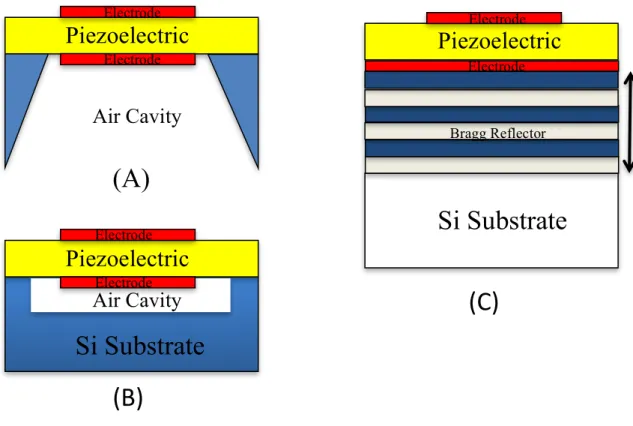
The most common configuration of a thin film bulk acoustic wave resonator (TFBAR) is based upon the standing bulk acoustic wave across the thickness of the piezoelectric layer sandwiched between two metal electrodes. This structure setup must be enclosed by acoustically insulating boundaries such that energy loss is minimized through the substrate and this is typically done by introducing an air cavity
or an acoustic reflector under the resonator.[33] Low cost substrates can be used
instead of piezoelectric substrates and can be potentially compatiable with Integrated Circuits & Systems. The typical frequency range of a FBAR resonator is from 1GHz
to 10GHz[31], such high frequency capabilities are becoming increasingly important in
today’s demanding communications sector.
Mechanical motion is initiated in the piezoelectric when an RF signal is applied across the device. Resonance occurs when the thickness of the film is equal to a
multiple of half the wavelength of the input signal shown below[34],
F
res=1/ λ
res=V
a/2d
(2.28)V
a=
!! (2.29)where Fres is the resonant frequency of the device, λres is the wavelength, d is the
thickness of the film, E is the Young’s Modulus, Va is the speed of a travelling wave
The resonator is one of the key components of frequency generation and selection applications of oscillators and filters. By applying an AC electric field to a piezoelectric crystal, acoustic waves will be excited that result in a resonance at a frequency determined by the mechanical properties and physical dimensions of the crystal. Since the resonance frequency of the piezoelectric resonators based on bulk acoustic waves depend on the crystal dimensions, the maximum frequency is mainly
related to the thickness of the piezoelectric crystal.[35]
It must be noted that the electrical performance of bulk acoustic wave (BAW) resonators depends on the piezoelectric layer and how the acoustic wave is confined in the structure. The acoustic waves are generated and reflected within the piezoelectric film due to the converse piezoelectric effect in bulk acoustic wave resonator as an AC electric field is applied. When half of the acoustic wavelength is equal to the thickness of the piezoelectric film, a mechanical standing wave is formed and resonance is observed. The thickness must be at odd number of half-wavelength for higher order resonances. The acoustic waves then polarize the material through the direct piezoelectric effect. The mechanically induced polarization at the standing
wave frequency is 180° out of phase with the dielectric polarization due to the
externally applied AC field. At this frequency, the current is minimized due to polarization charge cancelling out and gives a parallel type resonance at the electrical port. At a lower frequency, the two polarization charges are in phase and results are high current and a series resonance.
In an ideal scenario of bulk acoustic wave resonator with infinitely thin electrodes, the
thickness mode resonant frequency in series (fs) and parallel (fp) is given as the
following,[21]
f
!=
!!" !"=
! !" !!!! ! (2.30)f
!=
f
!1
−
!!!k
!! (2.31)k
!=
!!!! !!!! ! !! !(2.32)
where Vac is the acoustic wave velocity, t is the thickness of the ferroelectric film, ktis
the electromechanical coupling coefficient(k33), ρ is the density of the ferroelectric
piezoelectric film, !!!! is the permittivity coefficient and !
!! is the piezoelectric stress
coefficient.
The electrical impedance of a bulk acoustic wave resonator is characterized by the
resonances at the resonance frequency fr where the impedance value is at the
minimum and the resonances at the antiresonance frequency fa where the impedance
value is at infinity. This is illustrated in Figure 2.8. The BAW resonator behaves as an inductor when the phase at 90° and exhibit a capacitive behaviour when the phase reaches -90°.
Figure 2.8. Electrical input impedance of a BAW resonator[36] 2.2.1 State of Art of Ferroelectric Materials in BAW Resonators
Ferroelectric materials such as Strontium Titanate (STO) and Barium Strontium Titanate (BaxSr1-xTiO3) are promising candidate for bulk acoustic wave resonator with tunability, i.e a possibility to change the resonance frequency. Therefore, it would enable development of new components such as tunable filters, switches and voltage controlled oscillators. Ferroelectric materials are strong candidates for commercial tunable microwave frequency devices and applications, because of their fast tuning speeds, low cost, high power handling, miniaturization and potential for Si
integration.[37] The permittivity of ferroelectric materials can be changed
proportionally with the applied DC electric field, but it is limited to the Curie temperature as the phase change from ferroelectric to paraelectric. The main disadvantage for using ferroelectric materials in tunable microwave devices is the
relatively large dielectric loss tangent and associated microwave dissipation. However, recent literature, including our collaborators in Russia has suggested this loss tangent is due to interaction of microwave field with the phonons causing the excitation of bulk acoustic waves within the ferroelectric film and this microwave power loss can
be utilized to make a novel tunable bulk acoustic wave resonator.[1] This microwave
loss can also be reduced through improving thin film fabrication techniques, but the device tunability will decrease as well as the insertion loss.
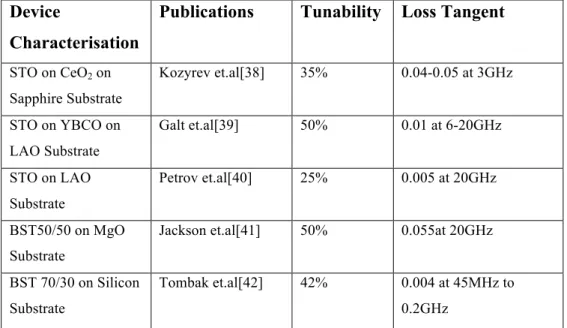
The microwave properties of these ferroelectric materials like STO and BST have been characterized by many research groups. A summary of the measured tunability and loss tangent is summarized in the table 2.2 and 2.3 below.
Device
Characterisation
Publications Tunability Loss Tangent STO on CeO2 on Sapphire Substrate Kozyrev et.al[38] 35% 0.04-0.05 at 3GHz STO on YBCO on LAO Substrate Galt et.al[39] 50% 0.01 at 6-20GHz STO on LAO Substrate Petrov et.al[40] 25% 0.005 at 20GHz BST50/50 on MgO Substrate
Jackson et.al[41] 50% 0.055at 20GHz BST 70/30 on Silicon
Substrate
Tombak et.al[42] 42% 0.004 at 45MHz to 0.2GHz
Table 2.2. A summary of the dielectric properties measurements reported for STO and BST films
Kozyrev et.al[38] reported the microwave properties of STO planar varactors on CeO2
buffered r-plane Al2O3 substrates using 200nm thick YBa2Cu3O7-x electrodes. The planar varactor was inserted into the gap at the midpoint of the resonator’s microstrip line, thus loading the resonator with an additional capacitance. The varactors are
made up of 1mm2 pads separated by 20µm gaps, which gave a capacitance of 0.4pF at
zero bias and is tuned to 0.26pF with 260V corresponding to electric field of
130kV/cm at 3GHz. The tan δ ranged from 0.04 to 0.05 at zero bias and was reduced
by a factor of 1.3 at higher bias voltages. This was one of the first reported STO device structures considered for electrically tunable microwave applications.
Galt[39] investigated the dielectric reporsponse of a microstrip resonator incorporated
![Figure 2.4. Temperature dependence of the loss tangent at zero biasing field for single crystal Strontium titanate at microwave frequeuncies [7]](https://thumb-us.123doks.com/thumbv2/123dok_us/11108814.2998655/23.892.180.707.107.470/figure-temperature-dependence-tangent-strontium-titanate-microwave-frequeuncies.webp)
![Figure 2.9. The dc bias dependence of a) resonant frequency and b) reflected power corresponding to two states (On and Off) at T=52K and dc field of 1.2kV/cm .[49]](https://thumb-us.123doks.com/thumbv2/123dok_us/11108814.2998655/40.892.185.716.428.654/figure-dependence-resonant-frequency-reflected-power-corresponding-states.webp)
![Figure 2.16. a)Difference between the DC and RF Sputtering System, b) the simple schematic of the magnetron sputtering system [94]](https://thumb-us.123doks.com/thumbv2/123dok_us/11108814.2998655/55.892.145.808.111.370/figure-difference-dc-sputtering-simple-schematic-magnetron-sputtering.webp)
![Figure 2.17. a)Electricial resisitivity vs Argon pressure for sputtered titanium films [97] and b)Zone Model showing the influence of argon pressure and substrate temperature on the microstructure of metal thin films [97]](https://thumb-us.123doks.com/thumbv2/123dok_us/11108814.2998655/56.892.160.742.425.720/electricial-resisitivity-pressure-sputtered-influence-substrate-temperature-microstructure.webp)
![Figure 2.26. A)Ion beam etching rate of different materials and b)Kaufman type ion beam etching system [117]](https://thumb-us.123doks.com/thumbv2/123dok_us/11108814.2998655/64.892.142.767.659.994/figure-ion-beam-etching-different-materials-kaufman-etching.webp)