Operational Transresistance Amplifier Based PID
Controller
Rajeshwari PANDEY
1, Neeta PANDEY
1, Saurabh CHITRANSHI
1, Sajal K. PAUL
21Department of Electronics and Communication Engineering, Shahbad Daulatpur, Delhi Technological University, Bawana Road, DL - 42, Delhi, India
2Department of Electronics Engineering, Indian School of Mines, Dhanbad – 826004, Jharkhand, India
[email protected], [email protected], [email protected], [email protected] DOI: 10.15598/aeee.v13i2.1164
Abstract.This paper presents Operational transresis-tance amplifier (OTRA) based proportional-integral-derivative (PID) controller with independent electronic tuning of proportional, integral, and derivative con-stants. The configuration can be made fully integrated by implementing the resistors using matched transistors operating in the linear region. Theoretical propositions are verified through SPICE simulations using 0.18µm
process parameters from MOSIS (AGILENT). In or-der to demonstrate the workability of the proposed con-troller, its effect on step response of an OTRA based second order system is analyzed and presented.
Keywords
OTRA, PD, PI, PID, second order system.
1.
Introduction
A controller monitors and modifies the operational con-ditions of a given dynamical system. These opera-tional conditions are referred to as measured output variables and can be modified by adjusting certain in-put variables. The controller calculates the difference between a measured output variable and a desired set point as an error value and attempts to minimize the error by adjusting the process control inputs. In gen-eral controllers can be classified as (i) conventional and (ii) non-conventional controllers. For conventional con-trollers, such as PID controller, a prior knowledge of the mathematical model of the process to be controlled is required in order to design a controller whereas for unconventional controllers this information is gener-ally not needed. P, PI, PD, and PID are few
typ-ical examples of conventional controllers, and neuro-fuzzy controllers are representatives of the unconven-tional class. The controllers based on proportional-integral-derivative (PID) algorithm are most popularly used in the process industries. These are used to con-trol various processes satisfactorily with proper tuning of controller parameters. Generally operational ampli-fiers (OPAMPs) are used to design classical analog con-trollers [1], [2]. However the OPAMPs, being voltage mode circuit, have their limitations of constant gain bandwidth product (fT) and low slew rate. This
in-accurately limits the speed of the OPAMP-based con-trollers and might influence the dynamics of the system [3]. It is well known that inherent wide bandwidth al-most independent of closed loop gain; greater linearity and large dynamic range are the key performance fea-tures of current mode technique [4]. Therefore, the current mode building blocks would be a good alter-native of OPAMP for designing the analog controllers. Literature survey reveals that number of current mode circuits have been reported relating to PID controllers [3], [5], [6], [7], [8]. Operational transconductance am-plifier (OTA) based controllers are proposed in [5] and are electronically tunable. However, these provide volt-age output at high impedance making a buffer nec-essary to drive the voltage input circuits. The cur-rent difference buffered amplifier (CDBA) based PID controller presented in [6] uses an excessively large number of active and passive components. References [3], [7], [8] present current conveyor II (CCII) based PID controllers. Two different structures are proposed for voltage and current outputs respectively in [7], [8] whereas [3] presents only voltage output configuration. All the CCII based voltage mode designs deliver output voltage at high impedance and are thus not suitable for driving voltage input circuits. The OTRA is yet an-other, relatively recently proposed current mode
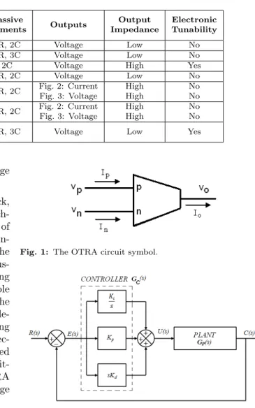
build-Tab. 1: Comparison of proposed work with existing literature. Reference Active block used No. of Active block used Passive elements Outputs Output Impedance Electronic Tunability
[1] Opamp 4 8R, 2C Voltage Low No
[3] Opamp 1 3R, 3C Voltage Low No
[5] OTA 8 2C Voltage High Yes
[6] CDBA 4 8R, 2C Voltage Low No
[7] CCII 3 4R, 2C Fig. 2: Current Fig. 3: Voltage
High High
No No [8] CCII 3 4R, 2C Fig. 2: Current
Fig. 3: Voltage High High No No Proposed
work OTRA 2 4R, 3C Voltage Low Yes
ing block which is a high gain current input, voltage output amplifier [9].
Being a current processing analog building block, it inherits the advantages of the current mode tech-nique. Additionally it is also free from the effects of parasitic capacitances at the input due to virtually in-ternally grounded input terminals [10] and hence the non-ideality problem is less in circuits implemented us-ing OTRA. Therefore, this paper aims at presentus-ing OTRA based PID controller with orthogonally tunable proportional, integral and derivative constants. The proposed circuit can be made fully integrated by imple-menting the resistors using MOS transistors operating in the non-saturation region. This also facilitates elec-tronic tuning of the controller parameters. A detailed comparison of the PID controllers available in the lit-erature is given in Tab. 1 which suggests that OTRA based structure is the most suitable choice for voltage mode operation.
2.
Proposed Circuits
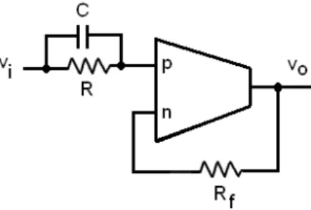
The OTRA is a three terminal device shown symboli-cally in Fig. 1 and its port relations can be character-ized by the matrix as follows:
Vp Vn V0 = 0 0 0 0 0 0 Rm −Rm 0 Ip In I0 , (1)
whereRmis the transresistance gain of the OTRA. For
ideal operations,Rmapproaches infinity and forces the
input currents to be equal. Thus, OTRA must be used in a negative feedback configuration [9], [10].
2.1.
PID Controller
In a given system the proportional action improves the rise time of the system, the integral action improves the steady-state error whereas the derivative action im-proves the degree of stability. So, none alone is capable
Fig. 1: The OTRA circuit symbol.
Fig. 2: Block diagram of a closed loop system with PID con-troller.
of achieving the complete improvement in system per-formance [11]. This leads to the motivation of using a PID controller so that the best features of each of the PI and PD controllers are utilized. In a PID con-troller as shown in Fig. 2 the proportional, integral and the derivative of the error signalE(s)are summed up to calculate the output actuating signal U(s) of the controller which controls the plant’s (GP(s)) function.
Thus, the transfer functionGC(s)of the PID controller
can be written as:
GC(s) =Kp+
Ki
s +sKd, (2)
where Kp, Ki, and Kd are the proportional, integral
and derivative constants respectively.
In the following subsection first an OTRA based PI controller is introduced followed by a PD controller. By combining these two controllers, the proposed PID controller is designed.
1) Proposed PI Controller
The PI controller comprises of proportional and in-tegral actions and can be derived from the controller block of Fig. 2 if the derivative block is excluded. The transfer function GP I(s), of the PI controller so ob-tained is given by:
GP I(s) =Kp+
Ki
s . (3)
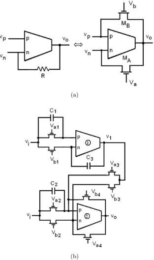
The OTRA based proposed PI controller is shown in Fig. 3.
Fig. 3: Proposed PI controller.
Using routine analysis the voltage transfer function of the proposed controller can be as expressed as:
GP I(s) = Vo Vi = C Cf + 1 s·Cf·R . (4)
From Eq. (4) the controller parameters can be com-puted as: Kp= C Cf , Ki= 1 R·Cf . (5)
It is clear from Eq. (5) that Kp value can be
ad-justed independently of Ki by varying C, andKi can
be independently controlled by varyingR.
2) Proposed PD Controller
A PD controller can be obtained if proportional and derivative actions only are taken into consideration in Fig. 2. Transfer function of a PD ControllerGP D(s),
can be represented as:
GP D(s) =Kp+s·Kd. (6)
Figure 4 shows the proposed PD controller circuit and the transfer function of this controller is obtained as: GP D(s) = Vo Vi =Rf R +s·C·R. (7)
The controller parameters can be expressed as:
Kp=
Rf
R , Kd=s·C·R. (8)
From Eq. (8) it is clear that by varyingR,Kpvalue
can be adjusted independently of Kd and by
simulta-neous variation ofRf andR such that Rf/Rremains
constant,Kd can be independently controlled.
Fig. 4: Proposed PD controller.
3) Proposed PID Controller
The proposed OTRA based PID Controller can be de-rived by combining the proposed PI and PD controllers and is shown in Fig. 5. The routine analysis of this cir-cuit gives the transfer function of the controller as:
GP ID(s) = Vo Vi == R4 R2 +R4·C1 R3·C1 + R4 s·C3·R1·R3 +s·C2·R4, (9)
from Eq. (9) the controller parameters can be identified as: Kp= R4·C1 R3·C3 +R4 R2 , Ki= R4 C3·R1·R3 , Kd=C2·R4. (10)
It is observed from Eq. (10) that the Kp value can
be adjusted independently by varyingR2, independent tuning ofKi is possible throughR1 variation whereas
Kd can be controlled independently by simultaneous
variation of R2, R3 and R4, such that R4/R2 and
R4/R3remain constant.
2.2.
MOS-C Implementation and
Electronic Tuning of the
Proposed Controllers
It is well known that the linear passive resistor con-sumes a large chip area as compared to the linear resis-tor implementation using transisresis-tors operating in the non-saturation region. The differential input of OTRA
Fig. 5: Proposed PID controller.
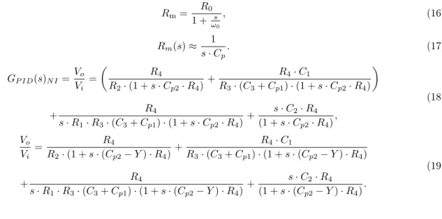
allows the resistors connected to the input terminals of OTRA to be implemented using MOS transistors with complete non-linearity cancelation [10]. Figure 6(a) shows a typical MOS implementation of resistance con-nected between negative input and output terminals of OTRA. The resistance value may be adjusted by ap-propriate choice of gate voltages thereby making con-troller parameters electronically tunable. The value of resistance so obtained is given by:
R= 1 µn·Cox· W L ·(Va−Vb) , (11)
whereVa andVb are control gate voltages; the
param-eters µn, Cox, W, and L represent electron mobility,
oxide capacitance per unit gate area, effective channel width, and effective channel length respectively and their value are expressed as:
µn = µ0 θ(VGS−VT) , (12) Cox= εox tox , (13) W =WDrawn−2WD, (14) L=LDrawn−2LD, (15)
where the symbols have their usual meaning.
The MOS transistors based implementation of lin-ear resistors not only reduces the chip area but also makes controller parameters electronically tunable. The MOS-C implementation of the circuit of Fig. 5 is shown in Fig. 6(b).
(a)
(b)
Fig. 6: MOS implementation of (a) linear resistance, (b) pro-posed PID controller.
3.
Nonideality Analysis of PID
Controller
The non-idealities associated with OTRA based cir-cuits may be divided into two groups. The first group results due to finite trans-resistance gain whereas the second one concerns with the nonzero impedances ofp
andnterminals of OTRA.
3.1.
Nonideality due to Finite
Transresistance Gain
Here the effect of finite transresistance gain (Rm) on
PID controller is considered, and passive compensa-tion is employed for high-frequency applicacompensa-tions. Ide-ally theRm is assumed to approach infinity. However,
practically Rm is a frequency dependent finite value.
Considering a single pole model for the trans-resistance gain, it can be expressed in Eq. (16):
Rm= R0 1 + s ω0 , (16) Rm(s)≈ 1 s·Cp . (17) GP ID(s)N I= Vo Vi = R 4 R2·(1 +s·Cp2·R4) + R4·C1 R3·(C3+Cp1)·(1 +s·Cp2·R4) + R4 s·R1·R3·(C3+Cp1)·(1 +s·Cp2·R4) + s·C2·R4 (1 +s·Cp2·R4) , (18) Vo Vi = R4 R2·(1 +s·(Cp2−Y)·R4) + R4·C1 R3·(C3+Cp1)·(1 +s·(Cp2−Y)·R4) + R4 s·R1·R3·(C3+Cp1)·(1 +s·(Cp2−Y)·R4) + s·C2·R4 (1 +s·(Cp2−Y)·R4) . (19)
where R0 is dc transresistance gain. For high-frequency applications the transresistance gain reduces to Eq. (17).
The termCprepresents parasitic capacitance
associ-ated with OTRA and is given by Cp=R0ω0. Taking this effect into account Eq. (9) modifies to Eq. (18), where Cp1 and Cp2 are the parasitic capacitances of OTRA1 and OTRA2 respectively.
For high-frequency applications, compensation methods must be employed to account for the error in-troduced in Eq. (9). The effect ofCp1can be eliminated by pre-adjusting the value of capacitors C3 and thus achieving self-compensation. The sCp2 term appear-ing in parallel toR4will result in the introduction of a parasitic pole having radian frequency asω= 1/R4Cp2. The effect ofCp2 can be eliminated by connecting an admittanceY between the non-inverting terminal and the output as shown in Fig. 7. Considering the circuit of Fig. 7, Eq. (18) modifies to Eq. (19).
By taking Y = sCp2, Eq. (19) reduces to Eq. (9) thus eliminating the effect ofCp2 and hence achieving the passive compensation.
3.2.
Effect of Nonzero Impedances of
p and n Terminals
Ideally the input as well as output resistances of an OTRA are assumed to be zero. Considering the in-put (Rn and Rp) and output (Ro) resistances of the
OTRA to be finite, the equivalent model of proposed PID controller can be drawn as shown in Fig. 8.
Routine analysis of circuit of Fig. 8 results in termi-nal currentsIp1 andIn1 as:
Ip1=
Vi·(1 +s·C1·R1)
R1+Rp1+s·C1·R1·Rp1
, (20)
Fig. 7: Compensated PID controller.
Ip1=
Vi·s·C3
1 +s·C3·Rn1
, (21)
whereIp1andIn1are the currents andRp1andRn1are the input resistances ofpandnterminals respectively of OTRA 1. ConsideringRm1to be the transresistance gain and Ro1 is the output resistance of OTRA1, the output voltage of OTRA1, can be computed as:
V10 =Rm1(Ip1−In1)−R0·In1, (22) V10=Rm1·Ip1−(Rm1+R0)·In1, (23) asRm1>> Ro1, so Rm1+Ro1≈Rm1and hence: V10=Rm1·(Ip1−In1), (24) V10 Vi = Rm1·(1 +s·C1·R1) R1+Rp1+s·C1·R1·Rp1 · 1 +s·C3·Rm1 1 +s·C3(Rm1+Rn1) , (25)
V10 Vi = (1 +s·C1·R1)·(1 +s·C3·Rm1) R1·(1 +s·C1·Rp1)· 1 Rm1 +s·C3 , (26) Vi0= (1 +s·C1·R1)·(1 +s·C3·Rm1)·Vi R1·(1 +s·C1·Rp1)·(s·C3) , (27) Ip2= V10R2+ViR3(1 +sC2R2) R2Rp2+R2R3+Rp2R3(1 +sC2R2) = V1 0R 2+ViR3(1 +sC2R2) R2(Rp2+R3) +Rp2R3(1 +sC2R2) ≈ V1 0R 2+ViR3(1 +sC2R2) R2R3+Rp2R3(1 +sC2R2) = V1 0R 2+ViR3(1 +sC2R2) R3(R2+Rp2) +sC2R2R3Rp2 ≈ V1 0 R3(1 +sC2Rp2) + Vi(1 +sC2R2) R2(1 +sC2Rp2) , (28) Ip2= (1 +sC1R1)(1 +sC3Rm1)Vi R1R3(1 +sC2Rp2)(1 +sC1Rp1)(sC3) + Vi(1 +sC2R2) R2(1 +sC2Rp2) . (29)
SubstitutingIp1andIn1, Eq. (24) results in Eq. (25). As R1 >> Rp1 and Rm1 >> Rn1, Eq. (25) yields to Eq. (26). It can be further simplified to Eq. (27) since
1/Rm1<<1.
From Fig. 8 Ip2, thepterminal current of OTRA2, can be written as Eq. (28), whereRp2is thepterminal resistance of OTRA2. Substituting for from Eq. (27)
Ip2can be expressed as Eq. (29)
Similarly consideringRn2to be thenterminal resis-tance of OTRA2 theIn2can be represented as Eq. (30) shown bellow:
In2=
Vo
R4+Rn2
, (30)
and the output voltage of OTRA2, can be computed as:
Vo=Rm2(Ip2−In2)−Ro2In2, (31) whereRm2andRo2are transresistance gain and output resistance of OTRA2 respectively. SinceRm2 >> R2, soRm2+Ro2≈Rm2 and hence Vo≈Rm2(Ip2−In2), (32) Vo= R4(1 +sC1R1)(1 +sC3Rn1)Vi R1R3sC3(1 +sC1Rp1)(1 +sC2Rp2) +R4(1 +sC2R2)Vi R2(1 +sC2Rp2) , (33)
and the transfer functionVo/Vi modifies to:
Vo Vi = 1 (1 +sC2Rp2) R 4C1(1 +sC3Rn1) R3C3(1 +sC1Rp1) +R4 R2 + R4(1 +sC3Rn1) R1R3sC3(1 +sC1Rp1) (1 +sC2Rp2) + sC2R4 (1 +C2Rp2) . (34)
It is observed from Eq. (34) that the nonzero val-ues of input resistances atnandpterminal of OTRAs result in introduction of parasitic pole and zero in pro-portional and integral terms and the derivative term consists of a parasitic pole. The numerical values of poles and zeros are very high as parasitic resistances of OTRA are very small. Thus, the parasitic zero and pole frequencies would not practically influence the sys-tem performance.
4.
Simulation Results
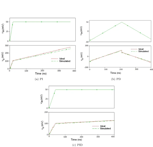
The theoretical propositions are verified through SPICE simulations using 0.18µm CMOS process pa-rameters provided by MOSIS. The CMOS implemen-tation of the OTRA, proposed in [13] with supply voltages ± 1.5 V was used for simulation. For per-formance evaluation of the proposed controllers, their time domain responses are obtained. The ideal and simulated time domain responses of the proposed PI controller of Fig. 3, for a 50 mV step input voltage with 20 ns rise time, are shown in Fig. 9(a). The passive component values of the PI controller are cho-sen as R = 50 kΩ, C = 4 pF and Cf = 2 pF and
the corresponding controller parameters are computed to be Kp = 2, Ki = 107 s−1. For transient
analy-sis of PD controller of Fig. 4, a 50 mV peak trian-gular input voltage is applied. The ideal and sim-ulated transient responses are depicted in Fig. 9(b). The component values for the PD controller are cho-sen as R = 10 kΩ, Rf = 20 kΩ and C = 20 pF and
the controller parameters are computed to beKp = 2,
Kd = 0.4 µs. For the PID controller of Fig. 5, values
of the capacitors are taken as C1 = C3 = 10 pF and
C2= 0.05 pF. The resistive component values are cho-sen as R1 = R2 = R3 = R4 = 50 kΩ. Using these passive component values various controller
parame-Fig. 8: Equivalent model of proposed PID controller.
(a) PI (b) PD
(c) PID
ters are computed as Kp = 2, Ki = 2 · 106 s−1 and
Kd = 2.5 ns. For time domain analysis, a 50 mV step
signal with 10 ns rise time is applied. The transient re-sponse of proposed PID controller is shown in Fig. 9(c). It is observed that for all the controllers the simulated and ideal responses are in close agreement.
5.
Performance Evaluation of
the Proposed Controllers
To evaluate the effect of various controllers, the per-formance of a second order plant is analyzed by form-ing a closed loop system as shown in Fig. 10(a) where
GP(s) represents the open loop transfer function of a
unity feedback system. For OTRA based realization of the closed loop system the low-pass filter (LPF) presented in [14] is used and is modified as shown in Fig. 10(b). The OTRA1, resistors R1, R2, along with capacitorsC1andC2form the second order plant whereas OTRA2 along with resistorsRaandRbis used
as subtractor thereby forming the error signal. The cir-cuit of Fig. 10 can also be made electronically tunable by implementing all the related resistors using MOS transistors operating in the linear region.
(a) Block diagram.
(b) OTRA based realization.
Fig. 10: Second order closed loop system.
The transfer function of the circuit of Fig. 10(b) us-ing equal component design with R1 = R2 = R and
C1=C2=Ccan be derived as:
Vo(s) Vi(s) = K R2C2 s2+ s CR+ K R2C2 , (35) where K= Rb Ra . (36)
The standard characteristic polynomial,D(s), of sec-ond order system [12] is given by:
D(s) =s2+ 2ξωns+ω2n, (37)
whereωn is the natural frequency of oscillations andξ
represents the damping factor. Comparing the denom-inator of Eq. (35) with Eq. (37) the ωn and ξ for the
LPF can be computed as:
ωn= √ K RC and ξ= 1 2√K. (38)
In the study that follows, the step response of the open loop second order system (LPF) is analysed first and then the effect of various proposed controllers on this second order system is observed by forming closed loop with controllers.
For the second order system shown in Fig. 10(b), the passive component values are chosen as
Ra = Rb = 20 kΩ,R1 = R2 = R3 = 2 kΩ, and
C1 = C2 =20 pF. Thefn andξfor the LPF can be
computed as 3.98 MHz and 0.5 respectively.
(a) with fixedξ
(b) with varyingξ
Fig. 11: Step Response of LPF.
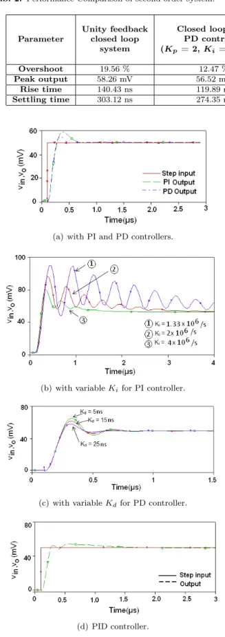
To observe the step response of the LPF a step in-put of 50 mV is applied, and the simulated response is shown in Fig. 11(a). The effect of damping ratio,ξon the step response of the second order LPF is shown in Fig. 11(b). To changeξ, Rb is kept constant whileRa
Tab. 2: Performance Comparison of second order system.
Parameter
Unity feedback closed loop
system
Closed loop with PD controller (Kp= 2,Ki= 107 s−1)
Closed loop with PI controller (Kp= 2,Kd = 0.4µs)
Closed loop with PID controller (Kp= 2, Ki= 2·106s−1, Kd= 2.5 ns) Overshoot 19.56 % 12.47 % 18.76 % 8.16 % Peak output 58.26 mV 56.52 mV 57.83 mV 52.59 mV Rise time 140.43 ns 119.89 ns 112.28 ns 99.75 ns Settling time 303.12 ns 274.35 ns 266.11 ns 252.27 ns
(a) with PI and PD controllers.
(b) with variableKifor PI controller.
(c) with variableKdfor PD controller.
(d) PID controller.
Fig. 12: Response of a second order system.
is varied electronically by changing gate voltages of the transistors used for implementing it. It is observed that
with the increase in ξ, oscillations are decreasing and is perfectly in tune with the theoretical concept. The performance of PI, PD, and PID controllers is evalu-ated by comparing step responses of closed loop sys-tems based on these controllers. Figure 12(a) depicts the effects of proposed PI (Kp = 2, Ki = 107 s−1)
and PD (Kp = 2, Kd = 0.4 µs) controllers on step
response of the closed loop system. Step response for varying values of Ki, while keeping Kp = 2 constant,
is depicted in Fig. 12(b). The effect of variable Kd
on the step response of the system, keeping Kp = 2
constant, is shown in Fig. 12(c). System step response with PID controller is represented by Fig. 12(d). Per-formance parameters such as overshoot, peak output, rise time and settling time of the closed-loop system with different controllers are measured and tabulated in Tab. 2. The study of the table clearly suggests that with the help of controllers the system performance is improved in a desired manner. The PD controller prominently improves the overshoot whereas PI con-troller influences mainly the settling time as compared to all other parameters. The PID includes best features of all individual controllers and results in improvement of all the performance measure parameters.
6.
Conclusion
Operational transresistance amplifier based PI, PD and PID controllers have been presented which possess the feature of independent tuning of proportional (Kp),
derivative (Kd) and integral (Ki) constants. By
imple-menting the resistors using MOS transistors operating in linear region MOS-C equivalent of the controllers can be obtained which are suitable for full integration. This also results in reduced chip area and power con-sumption as compared to passive resistors. To verify the functionality of the proposed controllers their ef-fect on a second order closed loop system was analyzed through simulations. The simulated results are in line with the proposed theory. The performance analysis reveals that PD controller improves percentage over-shoot, PI controller refines settling time while PID as a combination of the two, enhances transient as well as the steady-state response of the system.
References
[1] FRANCO, S. Design with operational amplifiers and analog integrated circuits. 3rd ed. Boston: McGraw-Hill, 2002. ISBN 00-723-2084-2.
[2] KARA, M. T. and M. E. RIZKALLA. Sin-gle op-amp proportional-integral compensator with antiwindup. In: 1993 IEEE International Symposium on Circuits and Systems. Chicago: IEEE, 1993, pp. 2260–2263. ISBN 0-7803-1281-3. DOI: 10.1109/ISCAS.1993.394212.
[3] MICHAL, V., C. PREMONT, G. PILLONET and N. ABOUCHI. Single active element PID con-trollers. In: 20th International Conference Ra-dioelektronika 2010. Brno: IEEE, 2010, pp. 1– 4. ISBN 978-1-4244-6318-3. DOI: 10.1109/RA-DIOELEK.2010.5478563.
[4] TOUMAZOU, C., F. J. LIDGEY and D. G. HAIGH. Analogue IC Design the Current Mode Approach. 1st ed. London: Peter Peregrinus on behalf of the Institution of Electrical Engineers, 1990. ISBN 08-634-1297-1.
[5] EDRAL, C., A. TOKER and C. ACAR. OTA-C Based Proportional- Integral-Derivative (PID) Controller and Calculating Optimum Parameter Tolerances. Turkish Journal of Electrical Engi-neering and Computer Sciences. 2001, vol. 9, no. 2, pp. 189–198. ISSN 1303-6203.
[6] KESKIN, A. U. Design of a PID Controller Circuit Employing CDBAs. International Jour-nal of Electrical Engineering Education. 2006, vol. 43, no. 1, pp. 48–56. ISSN 0020-7209. DOI: 10.7227/IJEEE.43.1.5
[7] MINAEI, S., E. YUCE, S. TOKAT and O. CICEKOGLU. Simple Realizations of Current-Mode and Voltage-Current-Mode PID, PI and PD Con-trollers. In:Proceedings of the IEEE International Symposium on Industrial Electronics. Dubrovnik: IEEE, 2005, pp. 195–198. ISBN 0-7803-8738-4. DOI: 10.1109/ISIE.2005.1528911
[8] YUCE, E., S. TOKAT, S. MINAEI and O.
CICEKOGLU. Low-Component-Count
In-sensitive Current-Mode and Voltage-Mode PID, PI and PD Controllers. Frequenz. 2006, vol. 60, no. 3–4, pp. 65–70. ISSN 2191-6349. DOI: 10.1515/FREQ.2006.60.3-4.65.
[9] CHEN, J. J., H. W. TSAO and C. C.
CHEN. Operational transresistance amplifier us-ing CMOS technology. Electronics Letters. 1992, vol. 28, no. 22, pp. 2087–2088. ISSN 0013-5194. DOI: 10.1049/el:19921338.
[10] SALAMA, K. N., A. M. SOLIMAN and C. C. CHEN. CMOS operational transresistance am-plifier for analog signal processing. Microelec-tronics Journal. 1999, vol. 30, no. 3, pp. 235– 245. ISSN 0026-2692. DOI: 10.1016/S0026-2692(98)00112-8.
[11] ASTROM, K. J., T. HAGGLUND and C. C. CHEN. The future of PID control.Control Engi-neering Practice. 2001, vol. 9, no. 11, pp. 1163– 1175. ISSN 0967-0661. DOI: 10.1016/S0967-0661(01)00062-4.
[12] GOLNARAGHI, M. and B. C. KUO. Automatic control systems.9th ed. Hoboken, NJ: Wiley, 2010. ISBN 978-047-0048-962.
[13] KAFRAWY, A. K. and A. M. SOLIMAN. A modified CMOS differential operational transre-sistance amplifier (OTRA). AEU - International Journal of Electronics and Communications.2009, vol. 63, no. 12, pp. 1067–1071. ISSN 1434-8411. DOI: 10.1016/j.aeue.2008.08.003.
[14] GOKCEN, A., S. KILINC and U. CAM. Sec-ond Order Analog Filter Design Using a Single OTRA Suitable for Integration. In: 15th Signal Processing and Communications Applications. Es-kisehir: IEEE, 2007, pp. 1–4. ISBN 1-4244-0719-2. DOI: 10.1109/SIU.2007.4298816.
About Authors
Rajeshwari PANDEYdid B.Tech. (Electronics and Telecommunication) from University of Allahabad, India, M.E. (Electronics and Control) from Birla In-stitute of Technology and Sciences, Pilani, Rajasthan, and Ph.D. from Delhi University, India.Currently, she is Associate Professor in Department of Electronics and Communication Engineering, Delhi Technological University, Delhi. Her research interests include Analog Integrated Circuits, and Microelectronics.
Neeta PANDEY did M.E. in Microelectronics from Birla Institute of Technology and Sciences, Pilani, Rajasthan, India and Ph.D. from Guru Gobind Singh Indraprastha University Delhi, India. At present she is Associate Professor in Department of Electronics and Communication Engineering, Delhi Technological University, Delhi. A life member of ISTE, and member of IEEE, USA, she has published papers in International, National Journals of repute and conferences. Her research interests are in Analog and Digital VLSI Design.
Saurabh CHITRANSI did B.Tech. (Electronics and Communication) from Uttar Pradesh Technical
University of Lucknow, India and M.Tech. (VLSI De-sign and Embedded System) from Delhi Technological University, Delhi, India. Currently, he is Executive Engineer in Diffusion and CVD Department, SITAR, DRDO, Bangalore, India. His research interests include Analog Integrated Circuits, MEMS and Silicon process integration.
Sajal K. PAUL did B.Tech., M.Tech., and Ph.D. in Radio Physics and Electronics from the Institute of Radio Physics and Electronics, University of Calcutta. He has served Webel Telecommunication Industries, Kolkata; Indira Gandhi National Open University
(IGNOU), Kolkata; Advanced Training Institute for Electronics and Process Instrumentation(ATI-EPI), Hyderabad; North Eastern Regional Institute of Sci-ence Technology(NERIST), Nirjuli and Delhi College of Engineering(DCE), Delhi in various capacities. He has served the Department of Electronics Engineering, Indian School of Mines, Dhanbad as Head of the Department and at present Professor of the same department. His research interest includes Microelec-toncic Devices, Electronic Properties of Semiconductor and Bipolar and MOS Analog Integrated Circuits. He has more than 60 research publications in International and National journals of repute and conferences.