A Dissertation by
VIKRAM SEKAR
Submitted to the Office of Graduate Studies of Texas A&M University
in partial fulfillment of the requirements for the degree of DOCTOR OF PHILOSOPHY
August 2011
A Dissertation by
VIKRAM SEKAR
Submitted to the Office of Graduate Studies of Texas A&M University
in partial fulfillment of the requirements for the degree of DOCTOR OF PHILOSOPHY
Approved by:
Chair of Committee, Kamran Entesari Committee Members, Robert D. Nevels
Laszlo B. Kish Debjyoti Banerjee Head of Department, Costas Georghiades
August 2011
ABSTRACT
Advances in Filter Miniaturization and
Design/Analysis of RF MEMS Tunable Filters. (August 2011) Vikram Sekar, B.E., Visveswariah Technological University;
M.S., Texas A&M University
Chair of Advisory Committee: Dr. Kamran Entesari
The main purpose of this dissertation was to address key issues in the design and analysis of RF/microwave filters for wireless applications. Since RF/microwave filters are one of the bulkiest parts of communication systems, their miniaturization is one of the most important technological challenges for the development of compact transceivers. In this work, novel miniaturization techniques were investigated for single-band, dual-band, ultra-wideband and tunable bandpass filters. In single-band filters, the use of cross-shaped fractals in half-mode substrate-integrated-waveguide bandpass filters resulted in a 37% size reduction. A compact bandpass filter that occupies an area of 0.315 mm2 is implemented in 90-nm CMOS technology for 20 GHz applications. For dual-band filters, using half-mode substrate-integrated-waveguides resulted in a filter that is six times smaller than its full-mode counterpart. For ultra-wideband filters, using slow-wave capacitively-loaded coplanar-waveguides resulted in a filter with improved stopband performance and frequency notch, while being 25% smaller in size.
A major part of this work also dealt with the concept of ‘hybrid’ RF MEMS tunable filters where packaged, off-the-shelf RF MEMS switches were used to imple-ment high-performance tunable filters using substrate-integrated-waveguide technol-ogy. These ‘hybrid’ filters are very easily fabricated compared to current state-of-the-art RF MEMS tunable filters because they do not require a clean-room facility. Both
the full-mode and half-mode substrate-integrated waveguide tunable filters reported in this work have the bestQ-factors (93−132 and 75−140, respectively) compared to any ‘hybrid’ RF MEMS tunable filter reported in current literature. Also, the half-mode substrate-integrated waveguide tunable filter is 2.5 times smaller than its full-mode counterpart while having similar performance.
This dissertation also presented detailed analytical and simulation-based studies of nonlinear noise phenomena induced by Brownian motion in all-pole RF MEMS tunable filters. Two independent mathematical methods are proposed to calculate phase noise in RF MEMS tunable filters: (1) pole-perturbation approach, and (2) admittance-approach. These methods are compared to each other and to harmonic balance noise simulations using the CAD-model of the RF MEMS switch. To ac-count for the switch nonlinearity in the mathematical methods, a nonlinear nodal analysis technique for tunable filters is also presented. In summary, it is shown that output signal-to-noise ratio degradation due to Brownian motion is maximum for low fractional bandwidth, high order and high quality factor RF MEMS tunable filters.
Finally, a self-sustained microwave platform to detect the dielectric constant of organic liquids is presented in this dissertation. The main idea is to use a voltage-controlled negative-resistance oscillator whose frequency of oscillation varies according to the organic liquid under test. To make the system self-sustained, the oscillator is embedded in a frequency synthesizer system, which is then digitally interfaced to a computer for calculation of dielectric constant. Such a system has potential uses in a variety of applications in medicine, agriculture and pharmaceuticals.
ACKNOWLEDGMENTS
A significant number of years has passed since my childhood days of pretending to be a scientist by collecting bugs, mixing “chemicals” I obtained from my mother’s kitchen and walking around with my father’s oversized white shirt and work gloves. My make-believe ideas were often fueled by “Dexter’s Laboratory”, a popular cartoon series in the nineties, about a boy genius who performed advanced scientific experi-ments in his hidden laboratory only to be destroyed by his clumsy sister. Those were probably the early roots of my scientific inquiry. Nearly two decades have passed, and I now have a completed doctoral dissertation. I cannot help but feel the end of my student years draw near while realizing that I have only managed to amass a tiny speck of knowledge from the vast multitude of existing information. Although learning is a lifelong process, there are several people I am thankful to, who helped me get to where my childhood dreams were.
Among these people is my Ph.D. advisor, Prof. Kamran Entesari, whose guidance has helped me develop my scientific rigor, rational thought and ideas through my years of advanced technical learning. His advice on various aspects of time management, technical analysis and scientific vision has helped me build a strong foundation for the future, which will aid me for many years to come. I would also like to thank my doctoral committee members, Prof. Robert D. Nevels, Prof. Laszlo B. Kish and Prof. Debjyoti Banerjee for all their assistance during my PhD program. I also thank Prof. Samuel Palermo for all the technical advice he provided during the development of the microwave sensor. I would also like to thank my colleagues and friends at Texas A&M University, especially Dr. Mohamed El-Nozahi, Mr. Ahmed A. Helmy, Mr. Marcelino Armendariz, Mr. Felix O. Fernandez, Dr. Raghavendra Kulkarni, Mr. William J. Torke, Mr. Hajir Hedayati, Mr. Mohamed Elkholy, and Mr. Ming-yi Li
for their help with measurement, design, fabrication and other matters. I would also like to thank Ms. Tammy Carda in the electrical engineering office for taking care of all my paperwork related issues, and Ms. Claudia Samford for assisting me in travel preparations.
I would like to thank my parents and family for their unwavering support from the early school years all through graduate school, and for their reassurance in difficult times. Finally, I would like to thank my wife for supporting me through graduate school, putting up with my long work hours, and making sure my graphs looked ‘pretty.’
TABLE OF CONTENTS
CHAPTER Page
I INTRODUCTION. . . 1
A. Filter Miniaturization . . . 5
B. RF MEMS Tunable Filters: Hybrid Approach and Noise Analysis . . . 9
C. Overview . . . 12
II NOVEL TECHNIQUES FOR FILTER MINIATURIZATION . . 15
A. Miniaturized UWB Bandpass Filters With Notch Using Slow Wave CPW Multiple Mode Resonators . . . 16
1. Introduction . . . 16
2. Initial UWB BPF . . . 17
a. Slow-Wave CPW MMR . . . 17
b. Stub-Loaded Transition with DGS Unit . . . 19
c. Measurements . . . 21
3. Slow-Wave UWB BPF with Notch . . . 23
4. Conclusion . . . 24
B. A K-Band Integrated Bandpass Filter in 90 nm CMOS Technology . . . 26
1. Introduction . . . 26
2. Filter Design . . . 27
a. Technology . . . 27
b. Meander-Line Inductor . . . 28
c. Filter Topology and Implementation . . . 30
d. Effect of Metal Filling . . . 33
3. Measurement Results . . . 33
4. Conclusion . . . 35
C. Miniaturized Half-Mode Substrate Integrated Waveg-uide Bandpass Filters Using Cross-Shaped Fractals . . . . 36
1. Introduction . . . 36
2. Design . . . 37
a. Fractal HMSIW Resonators . . . 37
b. Coupling . . . 40
CHAPTER Page
4. Conclusion . . . 46
D. A Novel Compact Dual-Band Half-Mode Substrate In-tegrated Waveguide Bandpass Filter . . . 47
1. Introduction . . . 47
2. Filter Synthesis . . . 48
a. Dual-Band Resonator . . . 48
b. Methodology . . . 49
3. Design and Implementation . . . 51
4. Fabrication and Measurements . . . 55
5. Conclusion . . . 57
III SUBSTRATE INTEGRATED WAVEGUIDE RF MEMS TUN-ABLE FILTERS. . . 58
A. Introduction . . . 58
B. A 1.2—1.6-GHz Substrate Integrated Waveguide RF MEMS Tunable Filter . . . 61
1. Tunable Resonator Structure . . . 61
a. SIW Cavity . . . 61
b. Tuning Mechanism . . . 63
c. Packaged RF MEMS Switch . . . 66
2. Tunable Resonator Design . . . 67
a. Resonance Contours . . . 67
b. External Quality Factor . . . 72
c. Tunable Cavity Implementation . . . 73
3. Filter Design . . . 77
4. Fabrication and Measurement . . . 79
a. Fabrication, Implementation and Biasing . . . 79
b. Measurements . . . 82
5. Spurious Suppression . . . 85
6. Nonlinear Characterization . . . 87
7. Conclusion . . . 90
C. Half-Mode Substrate Integrated Waveguide RF MEMS Tunable Filters . . . 91 1. Resonator Design . . . 91 a. HMSIW Model . . . 91 b. Tuning Mechanism . . . 93 c. Tuning Network . . . 95 d. Implementation . . . 97
CHAPTER Page
2. Filter Design . . . 101
a. Inter-Resonator Coupling . . . 101
b. External Coupling . . . 105
c. Complete Filter Simulation . . . 108
3. Fabrication and Measurement . . . 110
4. Conclusion . . . 116
IV NONLINEARITY AND NOISE ANALYSIS OF ALL-POLE RF MEMS TUNABLE FILTERS . . . 118
A. Introduction . . . 118
B. Nonlinear Noise Analysis of RF MEMS Tunable Filters Using Harmonic Balance Simulation∗ . . . 120
1. Brownian Motion Noise . . . 120
2. RF MEMS Tunable Filter . . . 121
3. Power Handling versus Bandwidth . . . 124
4. Phase Noise . . . 125
5. Higher Order Filters . . . 131
6. Conclusion . . . 136
C. Nonlinear Nodal Analysis of Tunable Microwave Filters . . 137
1. Introduction . . . 137
2. Theory . . . 138
3. Iterative Solution of Nonlinear Equations . . . 140
4. Nonlinear Varactor Model . . . 143
5. Case Study . . . 144
a. Nonlinear Reactance Deviations . . . 144
b. Peak Internal Voltage Distribution . . . 145
c. Large Signal S-Parameters . . . 145
6. Conclusion . . . 149
D. Pole Perturbation Theory for Nonlinear Noise Analysis of RF MEMS Tunable Filters . . . 150
1. Introduction . . . 150 2. Perturbation Theory . . . 151 a. Methodology . . . 152 b. Prototype Perturbation . . . 153 c. Pole Perturbation . . . 154 d. Discussion . . . 158
3. Nonlinear Noise Perturbation in RF MEMS Tun-able Filters . . . 158
CHAPTER Page
a. Nonlinear Analysis . . . 159
b. Noise Analysis . . . 160
c. Phase Noise Calculations . . . 163
4. RF MEMS Tunable Filter Example . . . 165
a. Design . . . 165 b. Nonlinearity . . . 168 c. Phase Noise . . . 170 5. Filter Nonidealities . . . 173 a. ResonatorQ-factor . . . 173 b. Nonideal Inverters . . . 176
6. Signal-to-Noise Ratio Analysis . . . 182
a. Basics . . . 183
b. Results . . . 185
c. Discussion . . . 186
7. Conclusion . . . 188
E. Unified Method of Nonlinear Noise Analysis Using the Method of Admittances . . . 189 1. Introduction . . . 189 2. Theory . . . 189 3. Filter Example . . . 192 4. Nonidealities . . . 193 a. ResonatorQ-Factor . . . 193 b. Frequency-Dependence of J-Inverters . . . 195 5. Conclusion . . . 197
V A SELF-SUSTAINED MICROWAVE PLATFORM FOR DE-TECTION OF ORGANIC LIQUIDS . . . 198
A. Introduction . . . 198
B. Fundamental Theory . . . 202
C. Oscillators for Dielectric Constant Measurement . . . 205
1. Oscillator Design . . . 205
a. Source Network . . . 207
b. Gate Network . . . 209
2. Response to Material Dielectric Constant . . . 210
3. Effect of Material Loss . . . 212
D. VCO Fabrication and Chemical Measurements . . . 215
E. Development of the Frequency Synthesizer System . . . 219
CHAPTER Page
2. Functionality . . . 220
3. Implementation . . . 223
F. Fully Self-Sustained Chemical Measurements . . . 227
1. Measurement Procedure . . . 229
2. Sensitivity Analysis . . . 230
3. Chemical Calibration and Detection . . . 232
G. Conclusion . . . 236
VI CONCLUSION AND FUTURE WORK. . . 237
A. Conclusion . . . 237
B. Future Work . . . 240
1. Half-Mode Substrate Integrated Waveguide Diplexer . 240 2. Ku-Band Half-Mode Substrate Integrated Waveg-uide RF MEMS Tunable Filter . . . 240
3. Experimental Verification of Nonlinear Noise in RF MEMS Tunable Filters . . . 241
4. Self-Sustained Platform for Detection of Material Loss 242 REFERENCES . . . 244
APPENDIX A . . . 260
APPENDIX B . . . 261
LIST OF FIGURES
FIGURE Page
1 UWB spectrum mask for indoor hand-held devices. . . 2 2 Block diagram of a multi-band wireless transceiver using RF MEMS
technology. . . 5 3 A substrate integrated waveguide formed by linear arrays of
metal-lic via-holes drilled in a planar substrate to emulate waveguide walls. 6 4 Metal-contact RF MEMS switches developed by (a) Radant MEMS
[40], (b) Omron Inc. [41], and (c) MIT Lincoln Laboratories [42]. . . 11 5 Three-dimensional view of the proposed UWB BPF with notch
using slow-wave CPW multiple-mode resonator (MMR). . . 17 6 Slow-wave CPW MMR and its equivalent circuit model. . . 18 7 Variation of loaded-line characteristic impedances, Z0,A/B,
nor-malized to the unloaded characteristic impedance Z0U, and the
change of resonance frequency of the first three modes of the
slow-wave CPW MMR against Lf. . . 20 8 (a) Stub-loaded transition with DGS unit, (b) improvement of
upper rejection skirt as the length of open stubs is increased, and (c) spurious suppression due to one DGS unit placed at the input
or output. . . 21 9 (a) Fabricated conventional and proposed UWB BPF prototypes,
(b) simulated/measured S-parameters of the conventional and pro-posed UWB BPF, and (c) simulated/measured group delay of the
FIGURE Page 10 (a) Proposed bridge structure over the slow-wave CPW MMR for
notch generation, (b) equivalent circuit model of the bridge, and (c) simulated response of Section B of CPW MMR with bridge and model parameters for various lengths of the bridge with Wb=0.2
mm, Wp=1 mm and d=0.6 mm. . . 23
11 (a) Fabricated UWB BPF with notch, and simulated/measured performance of the UWB BPF with notch—(b) S-parameters, (c)
group delay. . . 25 12 Layer configuration of the lumped inductors and capacitors in
IBM 90-nm CMOS process. . . 27 13 (a) Meander-line grounded inductor, (b) inductor equivalent
cir-cuit model, and (c) simulated inductance and quality factor vs.
frequency using Sonnet. . . 29 14 (a) Photograph of the fabricated two-port meander-line coupled
inductor structure in 90-nm CMOS process, and (b) resulting
S-parameters from the circuit model and measurements. . . 29 15 (a) Schematic of the two-pole Chebyshev bandpass filter, (b) top
view of the filter layout, (c) cross section ‘AA’, of the layout top
view, and (d) cross section ‘BB’ of the layout top view. . . 31 16 (a) Bandpass filter layout with dense metal filling around the filter
components, and (b) simulated filter response with and without
metal filling using Sonnet. . . 32 17 (a) Photograph of the fabricated bandpass filter in IBM 90-nm
CMOS process, and (b) simulated and measured S-parameters of
the bandpass filter. . . 34 18 (a) Conventional HMSIW resonator (0th-iteration), (b) the 1st
fractal iteration, and (c) the 2nd fractal iteration. . . 38 19 Simulated S21-parameters for various fractal iterations of the
FIGURE Page 20 Inductive input/output J-inverter for the (a) 0th-iteration, (b)
1st-iteration, and (c) 2nd-iteration, and (d) variation ofQextwith
hio for various fractal iterations. . . 40 21 Capacitive inter-resonator J-inverter for the (a) 0th-iteration, (b)
1st-iteration, and (c) 2nd-iteration, and (d) variation of k12 with
Lc for various fractal iterations. . . 42
22 Photographs of the fabricated filter prototypes. . . 43 23 Comparison between simulated and measured S-parameters for
(a) 0-th iteration, (b) 1st-iteration, and (c) 2nd-iteration HMSIW
bandpass filters. . . 44 24 A dual-band inverter coupled resonator. . . 49 25 (a) Generalized nth-order bandpass filter with ideal admittance
inverters, and (b) equivalent lowpass prototype network. . . 49 26 Synthesized response of the dual-band Chebyshev filter. . . 52 27 Geometrical structure of the proposed dual-band Chebyshev
HM-SIW BPF.. . . 52 28 (a) Photograph of the fabricated filter prototype, (b) measured
and simulated filter response, and (c) filter response up to 3.2 GHz. . 56 29 (a) Top view of the tunable SIW cavity using packaged RF MEMS
switches, (b)A−A0cross section of the tuning cavity, (c) top view of the tuning element employing an RF MEMS switch package, two tuning posts and a top via, and (d) B−B0 cross section of
the tuning element.. . . 62 30 (a) Photograph and structure of the packaged SPDT RF MEMS
switch, (b) side view of the SPST switch, (c) schematic of the
SPDT switch, and (d) measured S-parameters of the MEMS switch.. 65 31 Surface current distribution on the tuning post and vector
mag-netic field distribution within the cavity resonator at resonance
FIGURE Page 32 Magnitude of electric field distribution in the cavity at resonance
frequency, for various locations of tuning post; (a) disconnected post P near cavity center, and connected (b) post P near cavity center, (c) post Q near output port, (d) post R near input port,
and (e) post S away from ports and cavity center. . . 69 33 (a) Simulated magnitude of S21 for the tuning post configurations
in Fig. 32, and (b) resonance contours for a single tuning post
within the cavity. . . 71 34 Normalized variation of external quality factor for various
loca-tions of the tuning post with respect to (a) input port, and (b)
output port.. . . 73 35 (a) A tunable SIW resonator employing six tuning posts controlled
by three SPDT RF MEMS switch packages, and (b) coarse tuning
states obtained using only tuning posts ABCD. . . 74 36 Simulated resonant frequency of the SIW cavity for different
tun-ing states. . . 77 37 Simulated unloaded quality factor (Qu) of the SIW cavity for
dif-ferent tuning states. . . 78 38 Layout of the two-pole SIW RF MEMS tunable filter. . . 79 39 Simulated: (a) insertion loss and (b) return loss of the two-pole
1.2—1.6 GHz tunable SIW filter. . . 80 40 Fabricated 1.2—1.6 GHz SIW RF MEMS tunable filter. . . 81 41 Measured: (a) insertion loss and (b) return loss of the two-pole
1.2—1.6 GHz tunable SIW filter. . . 83 42 (a) Simulated/measured center frequency and measured insertion
loss. (b) Measured fractional bandwidth of the filter (3.7% ± 0.5%). 84 43 Comparison between the measured and simulated insertion loss
for three arbitrary states at 1.2 (State 1), 1.4 (State 8), and 1.6
FIGURE Page 44 Layout of the (a) two-pole SIW tunable filter employing LPFs at
the input/output for spurious suppression, (b) type-I LPF, and
(c) type-II LPF. . . 86 45 (a) Simulated wideband response of the tunable filter and lowpass
responses of Type-I and Type-II filters, and (b) spurious
suppres-sion for the lowest tuning state for various combinations of LPFs. . . 88 46 Measured wideband response of the 1.2—1.6 GHz tunable SIW
filter with spurious suppression. . . 89 47 (a) SIW with widthW operating in the TE10-mode with an
open-circuit along its symmetry plane, (b) higher order microstrip line with width W operating in the EH1-mode with a short-circuit along its symmetry plane, and (c) HMSIW with width W/2 as a
consequence of cases (a) and (b). . . 92 48 (a) Transverse equivalent network representation of the HMSIW
resonator. (b) HMSIW resonator with widthw=W/2 and length
L with via-holes of diameterd and spacing b. . . 92 49 (a) Transverse network representation, and (b) graphical
repre-sentation of resonance conditions of the HMSIW resonator.. . . 94 50 Complete circuit model of a tunable HMSIW resonator. . . 94 51 (a) Layout implementation of a tunable HMSIW resonator and
layout details for a pair of (b) coarse-tuning and (c) fine-tuning
branches. . . 98 52 Variation of resonance frequency and normalized admittance of
the tuning network for 15 different tuning states. . . 100 53 Implementation of the inter-resonator J-inverter. . . 102 54 Simulated electric and magnetic resonance peaks when two
HM-SIW resonators are weakly-coupled at the input/output for dif-ferent values of (a)w12, and (b)L12, and (c) variation of coupling
FIGURE Page 55 Variation of k12 versus tuning frequency of the resonator for
dif-ferent values of L12. In each case, w12 is adjusted to maintain
k12= 0.07 at the lowest tuning frequency. . . 104 56 Implementation of the input/output J-inverter and the
microstrip-to-HMSIW transition. . . 106 57 (a) Variation ofQe as a function ofwio and Lio, and (b) variation
of Qe versus tuning frequency of the resonator. In each case, wio
is adjusted to haveQe = 16.8 at the lowest tuning frequency.. . . 107
58 Simulated: (a) insertion loss and (b) return loss of the two-pole
1.2—1.6 GHz tunable HMSIW filter. . . 109 59 Fabricated 1.2—1.6 GHz HMSIW RF MEMS tunable filter. . . 110 60 Measured: (a) insertion loss and (b) return loss of the two-pole
1.2—1.6 GHz tunable HMSIW filter. . . 111 61 (a) Simulated/measured center frequency and insertion loss, and
(b) measured absolute 1-dB and 3-dB bandwidth of the filter. . . 112 62 Comparison between measured and simulated (a) insertion loss
and (b) return loss, for three arbitrary states at 1.2 (State 1), 1.4
(State 7), and 1.6 GHz (State 13). . . 114 63 Measured resonator unloaded quality factor (Qu). . . 115 64 Measured wideband response of the tunable HMSIW filter. . . 116 65 (a) A two-pole tunable bandpass filter, (b) three-bit RF MEMS
switched capacitor bank and (c) nonlinear electromechanical model
of the RF MEMS switch. . . 122 66 Simulated S21 of the tunable filter for fractional bandwidths of
0.5% and 5% for Q= 200. . . 124 67 Variation of RMS voltage across the switch with frequency for
different values of input power in a tunable filter of (a) 0.5%
FIGURE Page 68 Variation of RMS voltage across the switch with frequency for
different values of input power in a tunable filter of (a) 0.5%
frac-tional bandwidth and (b) 10% fracfrac-tional bandwidth. . . 127 69 Phase ofS21 versus frequency for the two-pole filter shown in Fig.
65(a) for different fractional bandwidths. . . 128 70 Variation of phase noise with input power and bandwidth, for
unloaded quality factor Q=100 and 200. Phase noise values are evaluated at Pin < Pin,max with all switches in the up-state
posi-tion and ω0 = 2π×13 kHz (ω0 < ωm). . . 129
71 Simulated phase noise for different tuning states of the filter. The tuning state (S1, S2, S3) = (0, 0, 0) shows the highest phase noise evaluated at Pin = 0 dBm (Pin < Pin,max), ω0 = 2π ×13 kHz
(ω0 < ωm) and Q=200. . . 131
72 Simulated phase noise as a function of mechanical frequency offset for different filter bandwidths. All switches are in the up-state
position, Pin = 0 dBm (Pin< Pin,max) and Q=200. . . 132 73 Three-pole tunable filter employing input/output capacitive
in-verters and inter-resonator inductive inin-verters. . . 133 74 Inductively-coupled lumped element tunable filter of order N. . . 133 75 Variation of phase noise with filter order for different fractional
bandwidths. All switches are in the up-state position. Phase noise is evaluated at Pin = 0 dBm (Pin < Pin,max) and ω0 = 2π×13
kHz (ω0 < ωm). . . 135 76 (a) Generalized all-pole Butterworth/Chebyshev bandpass filter
with ideal admittance inverters and lossless shunt resonators, and
(b) equivalent lowpass filter for a particular tuning state. . . 139 77 Recursive algorithm to find the nonlinear voltage distribution and
large signal s-parameters of a tunable filter. . . 142 78 N-pole lossless tunable filter implemented using GaAs varactors.
FIGURE Page 79 Nonlinear reactance deviations as a function of frequency for Case
A in (a) resonator 1, and (b) resonator 2, for different input powers.. 144 80 Nonlinear reactance deviations as a function of frequency for Case
B in (a) resonator 1, (b) resonator 2, (c) resonator 3 and (d)
resonator 4, for different input powers. . . 146 81 Voltage distribution for Case A across (a) resonator 1, and (b)
resonator 2, for different input powers, for different input powers. . . 147 82 Voltage distribution for Case B across (a) resonator 1, (b)
res-onator 2, (c) resres-onator 3, and (d) resres-onator 4, for different input
powers. . . 147 83 Large signal s-parameters for (a) Case A, and (b) Case B, for
different input powers. . . 148 84 (a) Generalized all-pole bandpass filter of orderN with ideal
ad-mittance inverters and lossless shunt resonators, and (b)
equiva-lent low-pass ladder network. . . 151 85 Distribution of poles on the complex s-plane for Butterworth
fil-ters with (a) odd order (eg. N=5) and (b) even order (eg. N=4). . . 155 86 Distribution of poles on the complex s-plane for Chebyshev filters
with (a) odd order (eg. N=5) and (b) even order (eg. N=4). . . 156 87 (a) A tunable RF MEMS shunt resonator, and (b) various
dis-placements in an RF MEMS shunt capacitive switch. . . 161 88 A tunable MEMS resonator implemented with P switched capacitors. 163 89 (a) AnN-pole lossless Butterworth/Chebyshev tunable filter with
ideal admittance inverters, (b) variable capacitor implementation using 2-bit RF MEMS switched capacitor banks, and (c) sim-ulated S-parameters of a lossless two-pole tunable Butterworth
FIGURE Page 90 (a) Nonlinear pole displacements in a two-pole Butterworth and
three-pole Chebyshev filter, (b) angular displacements of poles as a function of applied input power for different filter fractional bandwidths, and (c) group delay as a function of input power in two-pole Butterworth and three-pole Chebyshev filters for differ-ent filter fractional bandwidths. Theoretical values are compared
to large signal S-parameter (LSSP) simulations in ADS. . . 167 91 Phase noise of lossless two-pole Butterworth and three-pole
Cheby-shev filters as a function of input power for different fractional bandwidths, evaluated at an offset of ω0 = 2π×9 kHz (ω0 < ωm)
aroundf0 = 18 GHz. . . 170 92 Phase noise of lossless two-pole Butterworth and three-pole
Cheby-shev filters versus tuning state for different fractional bandwidths, evaluated at an offset ω0 = 2π×9 kHz (ω0 < ωm) from the center
frequency of that tuning state with Pin =−20 dBm. . . 171 93 Phase noise as a function of mechanical frequency offset around
f0=18 GHz in lossless two-pole Butterworth and three-pole
Cheby-shev filters for different fractional bandwidths at Pin=-20 dBm. . . . 172
94 Phase noise as a function of filter order for different fractional bandwidths of lossless Butterworth and Chebyshev filters, evalu-ated at an offset ω0 = 2π×9 kHz (ω0 < ωm) around f0=18 GHz
with Pin=-20 dBm. . . 173
95 (a) Displacement of poles to the left by δ due to losses present in the resonators of the tunable filter, and (b) Phase noise (Pph)
versus Qu for different fractional bandwidths in a two-pole
But-terworth and three-pole Chebyshev filter with noise calculation performed at a frequency offsetω0 = 2π×9 kHz (ω0 < ωm) around f0 = 18 GHz with Pin =−20 dBm and normalized to the phase
noise of the equivalent lossless filter. . . 175 96 Variation of phase noise versus input power in a two-pole
Butter-worth and three-pole Chebyshev filter with 1% fractional band-widths for Qu = 100 andQu = 500. Phase noise is evaulated at a
FIGURE Page 97 Equivalentπ-models for admittance inverters using (a) inductors,
and (b) capacitors. (c) Generalized lossy admittance inverter. . . 177 98 Comparison of phase noise versus tuning state in lossless
Butter-worth (N = 2) and Chebyshev (N = 3) filters with (a) 1% and (b) 8% fractional bandwidths employing ideal, capacitive and in-ductive inverters. Phase noise is evaluated with Pin =−20 dBm
at a frequency offsetω0 = 2π×9 kHz around the center frequency
of that tuning state. . . 178 99 (a) A lossless two-pole Chebyshev filter tunable from 15-18 GHz
with a constant fractional bandwidth of 8±0.1% with two-bit switched-capacitor bank implementations of (b) input/output ca-pacitor Cio, (c) resonator capacitance Cr and (d) inter-resonator
capacitanceCg. . . 179
100 Variation of phase noise with tuning state in a two-pole Chebyshev filter with a constant fractional bandwidth of 8±0.1% considering only noisy inverters, only noisy resonators and both noisy inverters and resonators. Phase noise is evaluated withPin=−20 dBm at
a frequency offsetω0 = 2π×9 kHz around the center frequency of that tuning state. The MEMS switch combinations for each state are also shown in the figure where ‘0’ and ‘1’ represent up- and
down-state positions, respectively.. . . 181 101 (a) Antenna and tunable filter in a 50 Ω system, (b) thermal
and phase noise when the received signal is weak (Thermal noise region: Pph,abs << Pth) and (c) thermal and phase noise when the
received signal is strong (Phase noise region: Pth << Pph,abs). . . 183
102 Total noise power and SNR calculated using harmonic balance in a 1-Hz bandwidth aroundf0 = 18 GHz for (a) Butterworth (N = 2) and, (b) Chebyshev (N = 3) filters versus received signal power (Pin), for different fractional bandwidths and quality factors, when
all switches are in the up-state position. The filter insertion loss
FIGURE Page 103 (a) Generalized all-pole Butterworth/Chebyshev tunable
band-pass filter with ideal admittance inverters and shunt resonators, (b) reduction of filter topology with respect to the ith resonator, and (c) simplified bandpass filter with theith noisy resonator and
complex terminating admittances. . . 190 104 Variation of filter phase noise for different fractional bandwidths
versus (a) input power, (b) mechanical frequency offset, (c) tuning state, and (d) filter order. Unless stated otherwise, phase noise is calculated at an offset of 2π×9 kHz at filter center frequency for
Pin =−20 dBm. . . 194
105 Variation of Butterworth filter phase noise with Qu for different
fractional bandwidths. Phase noise is calculated at an offset of
2π×9 kHz at filter center frequency for Pin =−20 dBm. . . 196
106 Comparison of phase noise in Butterworth filters versus tuning state for different inverter configurations for fractional bandwidths of (a) 1% and (b) 8%. Phase noise is calculated at an offset of
2π×9 kHz at filter center frequency for Pin =−20 dBm. . . 197
107 Real and imaginary components of complex permittivity for
com-mon organic liquids as predicted by the Debye model.. . . 204 108 Simplified schematic of the negative resistance oscillator used for
permittivity measurement. . . 205 109 (a) Simulation setup for the determination ofCs (DC biasing not
shown), (b) variation of magnitude of reflection coefficients at gate and drain withCs, and (c) phase variation of gate reflection
coefficient with frequency. . . 206 110 (a) Three-dimensional view of the sensing element, and (b)
di-mensions of the split-ring resonator (SRR). . . 208 111 Magnitude and phase variation of reflection coefficient of the gate
network as a function of the electrical length of the gate
FIGURE Page 112 Simulated: (a) phase of reflection coefficient of the gate network
caused by the presence of MUTs, and (b) change in oscillation
frequency and effective sensor capacitance versus dielectric constant. 211 113 Simulated: (a) Real part of sensor admittance when lossy, isotropic
MUTs with arbitrary 0r-value and various 00r-values are placed in the sample well. Oscillation condition in (5.4) as a function of 00r
for the case of (b) constant oscillation frequency and (c) constant
varactor voltage. . . 214 114 (a) Top-view of the fabricated permittivity-sensing oscillator
pro-totype, (b) side-view of the fabricated VCO, (c) measured oscil-lation spectrum without MUT, and (d) tuning characteristics of
the VCO. . . 216 115 (a) Measured oscillator frequency shift versus 0r for 10 µL MUT
samples. Error bars are shown only for calibration materials. (b) Error bars in measurement of MUTs for 10 µL sample volumes.
In both graphs, plotted symbols depict mean values. . . 217 116 (a) Measured oscillator frequency shift versus 0r for 20 µL MUT
samples. Error bars are shown only for calibration materials. (b) Error bars in measurement of MUTs for 20 µL sample volumes.
In both graphs, plotted symbols depict mean values. . . 218 117 Block diagram of a frequency synthesizer system digitally
inter-faced to a microcontroller unit. . . 221 118 Different phases of chemical detection using the frequency
synthe-sizer system. . . 222 119 Detailed implementation of the frequency synthesizer system with
a digital interface. . . 224 120 Schematic of the passive lowpass loop filter. . . 225 121 Schematic of the signal conditioning block. . . 226 122 Fabricated frequency synthesizer system for detection of organic
FIGURE Page 123 Measured frequency shift versus sample volumes for several MUTs. . 231 124 Chemical calibration curves for different sample volumes using air,
ethanol and methanol as reference materials.. . . 233 125 Extracted dielectric constant values for 2-butyl alcohol, o-xylene
and ethyl acetate for sample volumes between 10µL and 200 µL. . . 235 126 Block diagram of a dual-band receiver which uses a diplexer to
separate the received signal into appropriate frequency bands. . . 241 127 Frequency synthesizer architecture for organic liquid detection
LIST OF TABLES
TABLE Page
I Summary of Filter Performances (λg: Guided Wavelength at
Fil-ter CenFil-ter Frequency) . . . 45 II Final Dimensions of the Dual-Band HMSIW Filter . . . 55 III Cavity Parameters . . . 67 IV Positions of Tuning Posts (in mm) . . . 75 V Coarse and Fine Tuning Configurations . . . 76 VI ADS Model Element Values (r = 10.2, h = 0.635 mm, tanδ =
0.0023 at 10 GHz) . . . 99 VII Coarse and Fine Tuning Configurations (0:Open Switch, 1:Closed
Switch) . . . 100 VIII Filter Parameters for Different Filter Bandwidths . . . 123 IX Physical Dimensions and Electromechanical Parameters of the RF
MEMS Capacitive Switch . . . 123 X Resonator Model Element Values Used for ADS Simulations . . . 166 XI MEMS Switch Model Parameters . . . 166 XII Tunable Filter Model Element Values. . . 180 XIII Debye-Model Parameters for Organic Solvents @ 20◦C [112]. . . 203 XIV Comparison of the Extracted 0r Values with the Debye Model at
4.5 GHz . . . 219 XV Chemical Calibration Coefficients for the Frequency
TABLE Page XVI Comparison between Theoretical and Measured Values of
CHAPTER I
INTRODUCTION
Filters are among the most important components of communication and radar sys-tems, primarily due to their ability to select specific signal frequencies while rejecting unwanted interference. In the era of modern wireless communications, the frequency spectrum is a valuable resource that has been divided to serve a wide range of ap-plications. Conventionally, wireless systems only operate at a single frequency band allocated for that application. Thus, communication systems that operate at adja-cent frequency bands appear as interference to the narrowband system that must be rejected by appropriate filtering mechanisms. By selecting only a narrow range of frequencies around a desired signal frequency, the signal-to-noise ratio (SNR) of a narrowband communication system is greatly improved. Numerous books [1], [2] have been devoted to the design and implementation of single passband filters using a variety of microwave components such as waveguides, microstrip lines, striplines, etc.
For many applications, a single communication system may be required to work over multiple bands corresponding to several communication standards. The require-ments on such filters are much more stringent, and correspondingly their synthesis and design are much more involved. A trivial approach to filter design with multiple passband frequencies is to use a switched bank of single-passband filters in parallel combination. However, this approach often dramatically impacts size, cost and effi-ciency of the overall system and is avoided where possible. An elegant alternative is to design a single filtering structure that is capable of producing multiple passbands The journal model is IEEE Transactions on Microwave Theory and Techniques.
Fig. 1. UWB spectrum mask for indoor hand-held devices.
simultaneously. For this purpose, a variety of techniques have been developed for mul-tiple passband synthesis and have been implemented using waveguide and microstrip technologies [3], [4]. Since majority of the communication systems are inherently narrowband in nature, design techniques for single and multiple passband filters are generally limited to fractional bandwidths lower than 20% around the desired signal frequency.
Recently, the license-free assignment of the 3.1-10.6 GHz frequency range by the United States Federal Communications Commission (FCC) has pioneered the research and development of ultra-wideband (UWB) devices for low cost wireless sytems in military or commercial applications [5]. Fig. 1 shows the UWB spectrum mask for indoor hand-held devices specified by the FCC. UWB communication systems provide high bandwidth, reduced fading from multipath propagation and low power operation. For such applications, the design, implementation and fabrication of UWB filters used in UWB communication modules is a challenging problem when compared to narrow band systems primarily due to the very wide filter bandwidth (110% around center frequency of 6.85 GHz). In addition, the group delay flatness over the filter passband
is an important design parameter to avoid distortion of transmitted/received signals. An intuitive way to generate very wideband filters is to cascade highpass and lowpass filters with a corner frequencies at the lower and upper edges of the desired passband, respectively. A systematic procedure for the design of UWB filters using this approach is reported in [6]. However, a plethora of alternative design techniques have also been proposed which involve the use of multiple mode resonators [7], periodic structures [8], lumped elements on liquid crystal polymer [9], etc. A summary of these design techniques, along with their relative merits and demerits, is published in [10].
In addition to allocating the frequency spectrum according to fixed frequency bands, there is also a necessity to have narrowband filters whose center frequencies can be continuously changed. For example, in electronic support measures (ESM) systems, it may be required to classify the incoming signal according to frequency so that appropriate electronic countermeasures (ECM), such as signal-jamming, may be performed when necessary. To do this, the entire receive band is divided into smaller sub-bands and electronically scanned using a tunable filter with variable cen-ter frequency. In modern wireless communication systems, multi-band devices are becoming a major trend due to their ability to cover multiple standards using a sin-gle device [11]. Tunable filters are very important for such applications since they replace the use of a switched filter bank with a single component. Tunable filters are also essential components of “cognitive radios” which have the ability to change their network parameters (frequency, bandwidth, modulation) according to the available frequency spectrum for maximum data transfer. Most tunable filters belong to three basic types: mechanically tunable, magnetically tunable and electronically tunable.
Mechanically tunable bandpass filters are typically implemented using either coaxial or waveguide resonators [1], and offer large power handling capability with low insertion loss. However, their large size and slow tuning speeds render them
useless for modern highly integrated systems. Magnetically tuned filters typically employ Yttrium-Iron-Garnet (YIG) spheres in their resonators and are popular for their multi-octave tuning capability, spurious free response, low insertion loss and high quality factor (up to 10,000 in the 0.1 to 6 GHz range) [12]. However, their large size, slow tuning speed and high power consumption make them unacceptable in the context of modern low-power RF transceivers.
Electrically tunable filters use compact tunable capacitors as part of the res-onators so that the filter center frequency can be tuned very fast over a wide fre-quency range, making them ideal candidates for integrated RF front ends. Three major technologies are employed in electrically tuned filters [13].
(a) Semiconductor varactors: Varactor tuned filters rely on the change in
junc-tion capacitance when reverse bias is applied across the varactor diode. Although they exhibit superior tuning speed and have a compact size, they suffer from poor power-handling, significant non-linearity and poor quality factor at millimeter wave frequencies.
(b)Ferroelectric thin-film varactors: The ferroelectric nature of
Barium-Strontium-Titanate (BST) thin films has been used to develop a planar varactor technology that can be easily integrated with RF front ends. Much like semiconductor varactors, re-verse biasing the BST varactors results in a change in capacitance that is used to tune an RF filter. BST varactors are highly tunable at room temperature while having improved quality factors (60-100) and moderately nonlinear behavior.
(c) RF microelectromechanical systems (MEMS) switches: RF MEMS switches
are miniature devices which use mechanical movements to achieve an open- or short-circuit in a transmission line, and are actuated using electrostatic, thermal, magne-tostatic or piezoelectric mechanisms. Among these, electrostatic and piezoelectric mechanisms are widely used due to its simplicity, compactness and low power
con-Tuning network Tuning network LNA 0/90° Tuning network PA Tuning network Tunable antenna IF MEMS filter
MEMS tunable oscillator
Medium power amplifier From I/Q modulator SP2T To baseband MEMS tunable filter MEMS tunable filter MEMS tunable filter
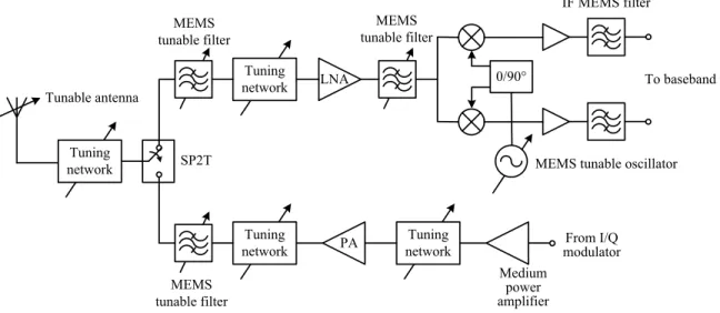
Fig. 2. Block diagram of a multi-band wireless transceiver using RF MEMS technology. sumption. Although MEMS switches have a moderate switching speed (3-100µs) and low power handling capability (1-2 W), they provide very low insertion loss (<0.2 dB) even up to 100 GHz, very high linearity (IIP3 >65 dBm), extremely low power con-sumption and very high isolation. They can also be integrated in a planar fashion with modern RF front-end electronics. Fig. 2 is an example of a multi-band wireless transceiver where tunability is implemented using RF MEMS technology.
The major themes of this dissertation are discussed in greater detail in the fol-lowing sections.
A. Filter Miniaturization
For applications where low-loss and high-selectivity are required, single- and dual-band filters have been implemented using waveguide technology in [1] and [14], re-spectively, since waveguide cavity resonators typically have very high quality factors (> 1000). However, such filters tend to be very bulky and expensive, and are not practical solutions for applications which require compactness. Planar,
transmission-Via h z y TE10-m ode d b
Fig. 3. A substrate integrated waveguide formed by linear arrays of metallic via-holes drilled in a planar substrate to emulate waveguide walls.
line based single- and dual-band filters are an excellent alternative when overall filter size is critical, and has emerged as a popular research topic in recent times. De-sign techniques for implementation of planar single passband filters using microstrip technology has been discussed in [15]. Several novel approaches have been developed to design dual-band filters which involve the use of stepped-impedance resonators (SIRs) [16], combline filters loaded with lumped series resonators [17] and reduced length parallel coupled lines [18]. While these techniques result in compact filters, the insertion loss performance and selectivity is relatively poor compared to their waveguide counterparts, primarily due to the low quality factor (100-150) of planar resonators.
Over the last decade, the search for middle ground between waveguide and pla-nar structures that provide high quality factor while still maintaining a relatively compact form-factor has given rise to the concept of substrate-integrated-waveguide (SIW) technology which was first introduced by Deslandes and Wu in [19]. Using SIW technology, waveguide components are implemented in planar substrates us-ing an array of closely spaced via holes to emulate the waveguide walls as shown in Fig. 3. As a consequence, relatively high resonator quality factors are achieved (300-400) using a technology that is relatively inexpensive to fabricate. Also, the
quasi-planar nature of SIWs makes it feasible for a lot of applications which require high performance filters but cannot tolerate the large size of conventional waveg-uide components. The excellent propagation characteristics of SIWs have resulted in rapid development of advanced single-band filtering structures that exhibit low insertion losses and good selectivity [20], [21]. In the context of multi-band filters, inverter-coupled bandpass/bandstop resonators have been utilized to implement dual passband filters using SIW technology in [22]. However, the size of SIW bandpass filters are still larger than their transmission-line based equivalents. Although there is some published work on the miniaturization techniques for SIWs in general [23], very little attention has been paid to miniaturization techniques for SIW filters to make them comparable in size to their planar counterparts while maintaining their excellent low-loss properties [24], [25]. Thus, one of the major purposes of this dis-sertation is to embark on the challenging issues of miniaturization of SIW filters, in an attempt to replace well-adopted planar filters with their SIW counterparts.
For UWB filters, high quality factor is not critical because the very wide frac-tional bandwidths involved often result in low insertion losses even for moderate quality factors. However, their miniaturization is still a primary concern. A variety of techniques have been proposed to design UWB filters, and a comprehensive review is provided in [10]. Among these, a configuration that has been increasingly popu-lar is based on the use of multiple-mode resonators (MMRs) to generate the UWB passband. Here, the multiple resonant modes of a microstrip or coplanar waveguide (CPW) resonator are designed to be quasi-equally distributed throughout the filter passband, and then strongly coupled to the input/output feed-lines using broadband coupling structures. In microstrip implementations [7], the coupling structures are implemented using parallel-coupled microstrip lines. However, to produce the nec-essary amount of coupling, the spacing between the coupled lines must be made
extremely narrow and hence imposes severe fabrication challenges. To overcome the fabrication complexity, composite microstrip-CPW transitions have been proposed in [26] that employ broadside coupling between microstrip and CPW lines to achieve tight coupling, and prove to be a feasible choice for easy implementation of UWB filters.
Within the 3.1-10.6 GHz communication band, there are a number of other communication standards operating at power levels that are much higher than that specified for UWB communication. To avoid interference between the UWB radio system and other narrowband standards present in the UWB frequency range, single-or multiple-notched bands are introduced in the UWB filter response. Several ap-proaches have been proposed to produce frequency notches in the UWB filter response including folded coupling fingers [27] and SIR resonators [28]. However, these struc-tures are difficult to incorporate into composite microstrip-CPW transitions without degrading the extent of coupling. Hence, new mechanisms for notch generation that are compatible with composite microstrip-CPW UWB filters are highly desired.
As specifications on system portability get more stringent, UWB filter miniatur-ization becomes a challenging problem considering that smaller size should not be accompanied by increased fabrication complexity. Thus, a part of this dissertation is devoted to developing techniques to miniaturize UWB filters, without increasing fabrication complexity, while producing interference rejection notches in the filter response and good out-of-band performance.
Besides the antennas, RF filters are generally the bulkiest parts of most commu-nication and radar systems. While the entire RF front-end electronics can be included in a single chip using modern integrated circuit (IC) technology, RF filters are mostly off-chip components that result in increased size and cost of the transceiver. From a system point of view, greatest miniaturization and cost-saving is achieved if the RF
filter is designed and implemented on-chip. While this approach has numerous advan-tages, various limitations pose challenging problems that need to be overcome before on-chip filters become a practical reality. First, the substrate losses in conventional IC processes such as complementary metal oxide semiconductor (CMOS) makes it difficult to realize high quality factor elements on chip. As a result, on-chip narrow-band filters often exhibit very high insertion losses. Second, the available area on-chip is very limited, and this makes transmission-line based approaches difficult to imple-ment on-chip due to their large size. Several distributed approaches to impleimple-menting on-chip passive filters have been reported in [29], [30] based on thin-film microstrip technology. However, these works have very large filter sizes even at frequencies of 60-and 77-GHz. Semi-lumped 60-and distributed approaches have been reported on CMOS technology in [31] and [32] that uses a multi-layer approach to implement compact on-chip filters. In this dissertation, techniques to implement K-band lumped-element filters will be studied in detail, in an effort to make fully-integrated system-on-chips feasible for 24-GHz Industrial-Scientific-Medical (ISM) unlicensed communication ap-plications.
B. RF MEMS Tunable Filters: Hybrid Approach and Noise Analysis
RF MEMS switches or varactors have a thin mechanical membrane suspended over a signal line, and provide a varying capacitance value depending on electrostatic or piezoelectric force applied to it. In varactors, application of an actuating force deforms the membrane, thereby continuously changing the capacitance between the membrane and signal line. However, MEMS varactors provide a narrow range of capacitance ratio (max/min ≈ 2), and are known to have poor reliability. On the other hand, MEMS switches provide only two values of capacitance depending on
whether the switch is in the up- or down-state position. When an actuating voltage is applied, the bridge collapses to its down-state thereby allowing the signal to pass through it. RF MEMS switches have better reliability and a much higher range of capacitance variation (max/min ≈ 20-100). Based on the type of contact made in the down-state position, MEMS switches are classified as metal-contact or capacitive switches. In both cases, when the switch is in the up-state position, it creates an open-circuit (Cup ≈ 6−80 fF). When in the down-state, a short circuit is created
using a metal-metal contact in metal-contact switches (Rs <2Ω) or a metal-dielectric
contact in capacitive switches (Cdown ≈1−2 pF). A detailed account of issues involved
in design and fabrication of RF MEMS switches in given in [33].
RF MEMS switches have been used to develop a variety of high performance tunable filters, and a comprehensive summary of the current state-of-the-art is pub-lished in [34]. A wide variety of planar RF MEMS tunable filters have been reported with unloaded quality factors between 50-150 [35]-[37]. By inserting monolithic RF MEMS capacitor modules into evanescent-mode waveguide cavities, very high quality factors between 300-400 have been obtained [38]. However, all these filters require extensive microfabrication in a clean-room environment which makes their implemen-tation very expensive and time-consuming. The detailed steps involved in fabrication of these filters are described in [39].
Recently, in an attempt to make RF MEMS switches more appealing to the automated-test equipment (ATE) industry, several efforts have been made to hermet-ically package these switches. Fig. 4 shows the packaged metal-contact RF MEMS switches developed by Radant MEMS [40], Omron Inc. [41], and MIT Lincoln Labo-ratories [42]. These switches have all been tested up to at least a 100 million cycles and have very good reliability. However, increased reliability comes at the cost of increased parasitic elements associated with the hermetic package. As a result, the
(a) (b) (c)
Fig. 4. Metal-contact RF MEMS switches developed by (a) Radant MEMS [40], (b) Omron Inc. [41], and (c) MIT Lincoln Laboratories [42].
quality factor of the packaged switches are lower than those of the actual switches themselves. This limits the use of packaged RF MEMS switches to the low-GHz fre-quency ranges, and results in very moderate performance when used with low quality factor elements such as transmission lines.
As discussed earlier, high quality factor resonators are easily obtained using SIW technology, while still being easy to fabricate using conventional printed circuit board technology. The use of packaged RF MEMS switches to develop tunable SIW filters gives rise to a new class of RF MEMS tunable filters with unprecedented performance that are very easy to fabricate and assemble. The concept of SIW “hybrid” RF MEMS tunable filters is relatively unexplored so far, and is one of the major goals of this dissertation.
As devices are scaled to the micro-scale, noise sources that are negligible in the macro-scale become significant and limit the performance of micro-devices. In RF MEMS switches, several noise sources impact switch performance including Brownian noise, acoustic noise, acceleration noise, and power supply noise [43] and are shown to have an impact on MEMS phase shifters and tunable filters [44]. From a system point of view, noise in RF MEMS tunable filters can have important SNR implications since they typically appear before the low-noise amplifier when used as band-select
filters. In current literature, the impact of Brownian noise on RF MEMS tunable filters has not been studied thoroughly although it can significantly impact system performance. In this dissertation, the effect of Brownian motion in RF MEMS tunable filters is presented in detail by developing fully-analytical, iterative and simulation-based methods to predict the level of signal degradation at the filter output.
C. Overview
The main purpose of this dissertation is two-fold. First, to develop state-of-the-art filter solutions for single/multi-band, ultra-wideband and tunable frequency alloca-tions with major emphasis on: (1) filter miniaturization, (2) high quality factor, (3) ease of fabrication and (4) good out-of-band performance. Second, to develop mathe-matical and simulation-based methods to derive fundamental limitations imposed by nonlinear noise in RF MEMS tunable filters. It also comprises the development of a self-sustained microwave platform for detection of organic liquids.
Chapter II focuses on miniaturization techniques for single-band, dual-band and UWB bandpass filters. First, methods to miniaturize composite microstrip-CPW UWB filters based on slow-wave capacitively-loaded CPW multiple-mode resonators are developed. A frequency notch is introduced using a bridge structure over the CPW resonator, and defected ground structures are used to improve the stopband performance. Second, a lumped-element K-band integrated filter is implemented in 90nm CMOS technology that is very compact compared to other reported on-chip passive filters at this frequency. Third, fractal structures are used to lower the size of half-mode SIW bandpass filters while simultaneously improving its quality factor. Finally, a very compact dual-band filter is implemented using half-mode SIW structures that results in a deep rejection notch between filter passbands, low insertion
loss and excellent upper stopband suppression.
Chapter III presents full-mode and half-mode hybrid SIW filters that are tunable from 1.2-1.6 GHz using discrete surface-mount RF MEMS switches. The SIW cavity resonators are tuned using via-holes to perturb the fields within the cavity. These fil-ters are designed to have either constant fractional or constant absolute bandwidths, and exhibit high quality factors are they are tuned. Techniques to improve the up-per stopband up-performance are also discussed in detail. It is shown that half-mode SIW tunable filters are much smaller than their full-mode counterparts while having comparable performance.
Chapter IV discusses the fundamental noise limits imposed by nonlinear noise in RF MEMS tunable filters, and their implications on SNR. First, a simulation-based approach is presented that employs the nonlinear model of the RF MEMS switch to predict nonlinear noise in RF MEMS tunable filters. Second, a nonlinear nodal analysis method customized to predict nonlinear effects in RF MEMS tunable filters without the use of computer-based techniques, is presented. Third, a mathematical approach to predict nonlinear noise in all-pole RF MEMS tunable filters is developed based on perturbation of the filter poles. The effect of filter nonidealities is discussed in detail. Finally, a unified approach to predict nonlinear noise in all-pole RF MEMS tunable filters is presented that is much simpler to use than the perturbation approach. Chapter V covers the design and implementation of a self-sustained microwave platform for the detection of lossy organic liquids. A novel technique to detect the dielectric constant of liquids based on microwave oscillators is presented. By using the microwave oscillator in a frequency synthesizer system, the whole measurement system is digitally interfaced to a computer and enables accurate determination of dielectric constant.
pro-vides a compact and high quality factor solution for many advanced filtering struc-tures, and can be used to develop diplexers with high rejection and isolation perfor-mance. A compact, low-loss, half-mode SIW tunable filter for 12-18 GHz applications is also proposed using RF MEMS switches which are monolithically fabricated along with the filter structure. Future research efforts must also be focused on experimental verification of the theories of nonlinear noise. The self-sustained detection platform must also be extended to detect the loss factor of materials, which is important for many practical applications.
CHAPTER II
NOVEL TECHNIQUES FOR FILTER MINIATURIZATION*
With the advent of wireless technology and ever increasing demand for high data rate mobile communications, the number of radios on mobile platforms have been steadily growing. Typically, each radio system is designed for a particular communication standard and requires the use of RF filters that select the required band of interest. In such cases, the overall size of each filter in the communication module must be as small as possible to reduce the overall size of the transceiver. Thus, techniques to miniaturize RF filters and reduce the overall circuit size are of vital importance. However, as it turns out, there is no generalized miniaturization technique that is equally applicable to all kinds of filtering structures. In this context, custom design techniques must be developed based on the actual filter topology for a particular application, that result in smaller filter sizes. As a result, as newer filtering struc-tures are developed to better suit the needs of a particular communication system, innovative filter miniaturization techniques are always required to make them smaller. In this chapter, miniaturization techniques are developed for single-band, dual-band and UWB dual-bandpass filters. First, slow-wave phenomena in capacitively loaded ∗c2011 IEEE. Part of this chapter is reprinted, with permission, from Vikram Sekar and Kamran Entesari, “Minia-turized UWB bandpass filter with notch using slow-wave CPW multiple-mode resonators,”IEEE Microwave and Wireless Components Letters,Feb. 2011.
c
2011 IEEE. Part of this chapter is reprinted, with permission, from Vikram Sekar and Kamran Entesari, “A K-band integrated bandpass filter in 90-nm CMOS technology,”IEEE Radio and Wireless Symposium,Phoenix, AZ, Jan. 2011.
c
2011 IEEE. Part of this chapter is reprinted, with permission, from Vikram Sekar and Kamran Entesari, “Minia-turized half-mode substrate integrated waveguide bandpass filters using cross-shaped fractals,”12th Annual IEEE Wireless and Microwave Conference (WAMICON),Clearwater, FL, Apr. 2011.
c
2011 IEEE. Part of this chapter is reprinted, with permission, from Vikram Sekar and Kamran Entesari, “A novel compact dual-band half-mode substrate integrated waveguide bandpass filter,”2011 IEEE International Microwave Symposium,Baltimore, MD, Jun. 2011.
coplanar waveguides are utilized to make the multiple-mode resonator used in UWB filters up to 40% smaller. Second, a very compact lumped element filter at K-band is designed and implemented on 90-nm CMOS technology. Lastly, miniaturization techniques for single-band and dual-band SIW filters are developed based on half-mode SIWs and cross-shaped fractals. For all cases, filter prototypes are fabricated and measured to validate the proposed design techniques.
A. Miniaturized UWB Bandpass Filters With Notch Using Slow Wave CPW Mul-tiple Mode Resonators
1. Introduction
Recently, there is increased interest in the development of ultra-wideband (UWB) systems operating between 3.1 to 10.6 GHz because they are capable of high data rates while consuming very low power. To this end, a variety of UWB filter topologies have been implemented to reject unwanted signal interference [10]. One popular approach is to employ stepped-impedance multiple-mode resonators (MMRs) using composite microstrip-coplanar waveguide (CPW) structures [26]. Since such filters are relatively large, there is a need for novel miniaturization schemes that result in filter sizes comparable to those in [45]-[48]. The UWB filters reported in [26]-[46] do not have broad upper stopbands with good rejection levels but this can be achieved in a compact way using defected ground structures (DGS) [47]. In addition, UWB filters employing composite microstrip-CPW structures such as those reported in [26]-[47] have no provision for generation of a frequency notch to reject WLAN interference.
In this section, a novel UWB filter using CPW MMR is presented with the fol-lowing advantages: (1) miniaturization using slow-wave CPW lines that result in 40% size reduction without DGS (25% with DGS) compared to the CPW MMR filter in
Open stubs Slow-wave CPW MMR DGS unit Microstrip-CPW transition Via-hole Notch structure Microstrip/Top layer CPW/Bottom layer
Fig. 5. Three-dimensional view of the proposed UWB BPF with notch using slow-wave CPW multiple-mode resonator (MMR).
[26], and comparable size to the slow-wave UWB microstrip filter in [48], (2) fre-quency notch generation using a novel bridge structure to reject WLAN interference, and (3) good upper skirt selectivity using stub-loaded microstrip-CPW transition and improved upper stopband rejection of greater than 22 dB from 11 to 16 GHz using DGS.
Fig. 5 shows the layout of the proposed UWB BPF with notch employing a slow-wave CPW MMR etched in the bottom layer which consists of CPW lines loaded with interdigital capacitors to create the slow-wave effect [49]. The slow-wave MMR is excited by a broadband microstrip to CPW transition to which open-ended stubs are attached to improve the upper skirt selectivity by introducing a transmission zero in the upper stopband. DGS units are located in the ground plane of the microstrip feed line to improve the upper stopband rejection. To produce a notch in the transmission response at a desired frequency, a novel bridge structure is etched in the top layer and connected to the bottom layer through via holes.
2. Initial UWB BPF a. Slow-Wave CPW MMR
Fig. 6 shows the slow-wave CPW MMR consisting of cascaded capacitively-loaded CPW lines indicated by Sections A and B, and the corresponding MMR equivalent
λg/4 λg/2 λg/4 Open Yin = 0 Equivalent model Sec. A Z0,A Sec. B Lf sA sB LA LB w w s wc g s Z0,B Z0,A Sec. A
Fig. 6. Slow-wave CPW MMR and its equivalent circuit model.
model. The fringing capacitance between interdigital fingers results in a higher ca-pacitance per unit length of the CPW line, and the electrical length of the resonator which is proportional toβ =ω√LC, is increased. Conversely, the required physical length of a CPW line for a given electrical length is smaller and hence results in miniaturization. Also, the characteristic impedance of the CPW line decreases be-cause Z0 =
q
L/C. Thus, the characteristic impedance and electrical length of each Section in the CPW MMR are controlled by appropriately choosing the number of fingers and the spacing between them, for a fixed finger length. The slow-wave CPW MMR design procedure is as follows: First, a standard high impedance CPW line is designed, typically around 70 Ω so that reasonable impedances are achieved after capacitive loading. Next, Section B of the slow-wave MMR is designed by maximally loading the CPW line using an arbitrary finger length Lf for greatest
miniaturiza-tion and lowest impedance, Z0,B. The number of fingers is chosen so that Section
B is λg/2-long at mid-band frequency. The minimum achievable size is ultimately
limited by fabrication tolerances. The characteristic impedance of Section A, Z0,A,
is determined using the equivalent model so that the resonant modes satisfying the condition Yin = 0 are quasi-equally distributed in the filter passband. Section A is
then designed by adjusting the number and spacing of the fingers so that its electrical length isλg/4 and characteristic impedance isZ0,A. The gapg at the open ends of the
resonators must be large enough to minimize parasitic capacitance to ground. Finally, the resonator is fine-tuned by adjustingLf till the required resonance frequencies are
obtained. Fig. 7 shows the variation ofZ0,A/B normalized to the unloaded impedance
of the CPW line (Z0U), and the corresponding change in the first three resonant
fre-quencies of the slow-wave MMR as a function ofLf. By choosing Lf = 1.2 mm, the
first three resonant frequencies of the CPW MMR are 4.13 GHz, 6.85 GHz and 9.57 GHz, when Z0,A = 47.3 Ω and Z0,B = 24.5 Ω at 6.85 GHz.
Full-wave simulations show that the slow-wave CPW lines exhibit bandgap be-havior around 22 GHz. Hence, Z0,A/B and normalized phase constants (β/k0) of the CPW lines are almost constant over the filter passband, since it is far away from the bandgap frequency [48]. Any Z0-variation over the passband range affects both
Z0A and Z0B so that their ratio remains constant, and hence the MMR resonant
frequencies are unchanged due to frequency dispersion. The final dimensions of the slow-wave CPW MMR design on 0.635 mm thick RT/Duroid 6010 with r = 10.2
are: wc = 2 mm, w = s =sB = 0.2 mm, sA = 0.7 mm, Lf = 1.2 mm, g = 0.8 mm,
LA = 2.45 mm and LB = 4.4 mm. The proposed slow-wave MMR is 40% smaller than the CPW MMR in [26].
b. Stub-Loaded Transition with DGS Unit
To design a UWB passband using the resonant modes of the slow-wave MMR, tight broadband-coupling between the feed lines and the slow-wave MMR is achieved with a broadside microstrip-CPW transition as shown in Fig. 8(a). The microstrip line on the top layer is coupled to the center conductor of the CPW on the bottom layer, and the coupling strength is higher if the length (L) and width (W) of the microstrip
f3
f2
f1
Fig. 7. Variation of loaded-line characteristic impedances, Z0,A/B, normalized to the
unloaded characteristic impedanceZ0U, and the change of resonance frequency
of the first three modes of the slow-wave CPW MMR againstLf.
line is increased. To improve the upper rejection skirt of the filter, two open-ended stubs with lengthsLs are attached to the top microstrip line to independently control
the upper transmission zero produced by the transition. The broadband transition is initially designed with Ls = 0 by increasing L and W till the coupling bandwidth
covers the UWB passband. The upper transmission zero is then brought closer to the upper passband edge by increasing the length of the stubs resulting in improved roll-off of the upper rejection skirt. Fig. 8(b) shows the S-parameters of the stub-loaded microstrip-CPW transition for different values of Ls. The final dimensions of
the stub-loaded transition are: L= 3.5 mm,W = 0.5 mm and Ls= 1.3 mm.
To improve the upper stopband suppression of the UWB filter, dumb-bell shaped DGS units are etched in the ground plane of the microstrip feed lines as shown in Fig. 8(a), so that each DGS unit resonates at the spurious frequency. As seen later, using
W d2 d1 s1 s2 gd Ls Ls L W L = 3.5 mm, W = 0.5 mm DGS Unit Open Stub (a) (b) (c) Dimensions in mm. s1 = 0.1 mm, d1 = 1.1 mm
Fig. 8. (a) Stub-loaded transition with DGS unit, (b) improvement of upper rejection skirt as the length of open stubs is increased, and (c) spurious suppression due to one DGS unit placed at the input or output.
a single DGS unit at the input and output of the filter results in a stopband rejection of greater than 20 dB from 11 to 16 GHz. Greater suppression can be achieved by increasing the number of DGS units, at the cost of larger filter area. Fig. 8(c) shows the S-parameters of the stub-loaded transition with DGS unit for different values ofs2 and d2. The optimized values of the DGS unit are: s1=0.1 mm, s2=0.4 mm, d1=1.1 mm,d2=1.35 mm and gd=1.2 mm.
c. Measurements
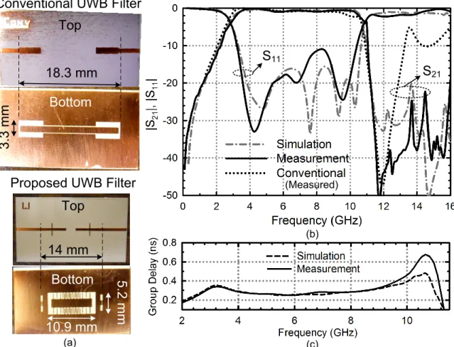
Fig. 9(a) shows the conventional and proposed UWB BPFs fabricated on 0.635 mm thick RT/Duroid 6010 substrate withr = 10.2. The proposed UWB BPF including DGS is 25% smaller in length compared to the conventional filter without DGS in [26]. The proposed UWB BPF was measured using an Anritsu 3680-20 Universal Test
(b)
(c) (Measured)
S11
S21 Conventional UWB Filter
Proposed UWB Filter 18.3 mm Top Bottom 3. 3 m m 10.9 mm 14 mm 5.2 m m (a) Top Bottom
Fig. 9. (a) Fabricated conventional and proposed UWB BPF prototypes, (b) simu-lated/measured S-parameters of the conventional and proposed UWB BPF, and (c) simulated/measured group delay of the proposed UWB BPF.
Fixture. The simulated/measured filter response and group delay are shown in Fig. 9(b) and (c), respectively. The proposed UWB BPF has a return loss better than 10-dB over the 3.1-10.6 GHz bandwidth with an insertion loss of 0.9 dB. The upper stopband suppression is better than 22 dB from 11 to 16 GHz and the group delay variation is relatively flat over the UWB passband. In comparison, the conventional UWB BPF has very poor stopband performance due to unsuppresed spurious modes.