1.
General description
The SC16C754B is a quad Universal Asynchronous Receiver/Transmitter (UART) with
64-byte FIFOs, automatic hardware/software flow control, and data rates up to 5 Mbit/s
(3.3 V and 5 V). The SC16C754B offers enhanced features. It has a Transmission Control
Register (TCR) that stores receiver FIFO threshold levels to start/stop transmission during
hardware and software flow control. With the FIFO Ready (FIFO Rdy) register, the
software gets the status of TXRDY/RXRDY for all four ports in one access. On-chip status
registers provide the user with error indications, operational status, and modem interface
control. System interrupts may be tailored to meet user requirements. An internal
loopback capability allows on-board diagnostics.
The UART transmits data, sent to it over the peripheral 8-bit bus, on the TX signal and
receives characters on the RX signal. Characters can be programmed to be 5, 6, 7, or
8 bits. The UART has a 64-byte receive FIFO and transmit FIFO and can be programmed
to interrupt at different trigger levels. The UART generates its own desired baud rate
based upon a programmable divisor and its input clock. It can transmit even, odd, or no
parity and 1, 1.5, or 2 stop bits. The receiver can detect break, idle, or framing errors,
FIFO overflow, and parity errors. The transmitter can detect FIFO underflow. The UART
also contains a software interface for modem control operations, and has software flow
control and hardware flow control capabilities.
The SC16C754B is available in plastic LQFP64, LQFP80 and PLCC68 packages.
2.
Features
n
4 channel UART
n
5 V, 3.3 V and 2.5 V operation
n
Pin compatible with SC16C654IA68, TL16C754, and SC16C554IA68 with additional
enhancements, and software compatible with TL16C754
n
Up to 5 Mbit/s data rate (at 3.3 V and 5 V; at 2.5 V maximum data rate is 3 Mbit/s)
n
5 V tolerant on input only pins
1n
64-byte transmit FIFO
n
64-byte receive FIFO with error flags
n
Industrial temperature range (−40
°C to +85
°C)
n
Programmable and selectable transmit and receive FIFO trigger levels for DMA and
interrupt generation
FIFOs
Rev. 04 — 6 October 2008
Product data sheet
n
Software (Xon/Xoff)/hardware (RTS/CTS) flow control
u
Programmable Xon/Xoff characters
u
Programmable auto-RTS and auto-CTS
n
Optional data flow resume by Xon any character
n
DMA signalling capability for both received and transmitted data
n
Supports 5 V, 3.3 V and 2.5 V operation
n
Software selectable baud rate generator
n
Prescaler provides additional divide-by-4 function
n
Fast data bus access time
n
Programmable Sleep mode
n
Programmable serial interface characteristics
u
5, 6, 7, or 8-bit characters
u
Even, odd, or no-parity bit generation and detection
u
1, 1.5, or 2 stop bit generation
n
False start bit detection
n
Complete status reporting capabilities in both normal and Sleep mode
n
Line break generation and detection
n
Internal test and loopback capabilities
n
Fully prioritized interrupt system controls
n
Modem control functions (CTS, RTS, DSR, DTR, RI, and CD)
n
Sleep mode
3.
Ordering information
Table 1. Ordering information
Type number Package
Name Description Version
SC16C754BIBM LQFP64 plastic low profile quad flat package; 64 leads; body 7×7×1.4 mm SOT414-1 SC16C754BIB80 LQFP80 plastic low profile quad flat package; 80 leads; body 12×12×1.4 mm SOT315-1 SC16C754BIA68 PLCC68 plastic leaded chip carrier; 68 leads SOT188-2
4.
Block diagram
Fig 1. Block diagram of SC16C754B
DTRA to DTRD RTSA to RTSD TRANSMIT FIFO REGISTERS TXA to TXD RECEIVE SHIFT REGISTER RECEIVE FIFO REGISTERS RXA to RXD INTERCONNECT B US LINES AND CONTR OL SIGNALS SC16C754B TRANSMIT SHIFT REGISTER XTAL2 XTAL1 002aaa866 INTSEL FLOW CONTROL LOGIC CLKSEL DATA BUS AND CONTROL LOGIC REGISTER SELECT LOGIC INTERRUPT CONTROL LOGIC D0 to D7 IOR IOW RESET A0 to A2 CSA to CSD INTA to INTD TXRDY
RXRDY CLOCK AND
BAUD RATE GENERATOR MODEM CONTROL LOGIC CTSA to CTSD RIA to RID CDA to CDD DSRA to DSRD FLOW CONTROL LOGIC
5.
Pinning information
5.1 Pinning
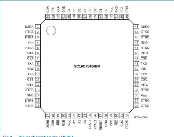
Fig 2. Pin configuration for LQFP64
SC16C754BIBM DSRA DSRD DTRA DTRD VCC RTSA RTSD INTA INTD TXA TXD IOW IOR TXB TXC CSB INTB INTC RTSB RTSC GND VCC DTRB DTRC CTSB DSRB CDA CDB RIA RIB RXA GND VCC D7 A2 D6 A1 D5 A0 D4 XTAL1 D3 XTAL2 D2 RESET D1 GND D0 RXC VCC RIC RXD CDC DSRC CDD 002aab564 1 2 3 4 5 6 7 8 9 10 11 12 13 14 15 16 48 47 46 45 44 43 42 41 40 39 38 37 36 35 34 33 17 18 19 20 21 22 23 24 25 26 27 28 29 30 31 32 64 63 62 61 60 59 58 57 56 55 54 53 52 51 50 49 GND RXB RID CTSA CSA CTSC CSC CSD CTSD
Fig 3. Pin configuration for LQFP80 SC16C754BIB80 n.c. n.c. n.c. DSRD DSRA CTSD CTSA DTRD DTRA GND VCC RTSD RTSA INTD INTA CSD CSA TXD TXA IOR IOW TXC TXB CSC CSB INTC INTB RTSC RTSB VCC GND DTRC DTRB CTSC CTSB DSRC DSRB n.c. n.c. n.c. n.c. n.c. n.c. CDA CDB RIA RIB RXA RXB GND CLKSEL D7 n.c. D6 A2 D5 A1 D4 A0 D3 XTAL1 D2 XTAL2 D1 RESET D0 RXRDY INTSEL TXRDY VCC GND RXD RXC RID RIC CDD CDC n.c. n.c. n.c. 1 2 3 4 5 6 7 8 9 10 11 12 13 14 15 16 17 18 19 20 60 59 58 57 56 55 54 53 52 51 50 49 48 47 46 45 44 43 42 41 21 22 23 24 25 26 27 28 29 30 31 32 33 34 35 36 37 38 39 40 80 79 78 77 76 75 74 73 72 71 70 69 68 67 66 65 64 63 62 61 002aaa867
5.2 Pin description
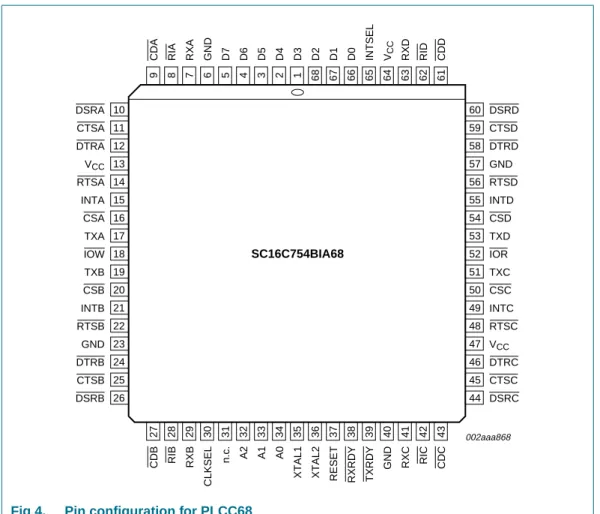
Fig 4. Pin configuration for PLCC68
SC16C754BIA68 DSRA DSRD CTSA CTSD DTRA DTRD VCC GND RTSA RTSD INTA INTD CSA CSD TXA TXD IOW IOR TXB TXC CSB INTB RTSB GND DTRB CTSB DSRB CSC INTC RTSC VCC DTRC CTSC DSRC CDB GND RIB D7 RXB D6 CLKSEL D5
CDA RIA RXA
n.c. D4 A2 D3 A1 D2 A0 D1 XTAL1 D0 XTAL2 INTSEL
RESET RXRDY TXRDY
GND RXC RIC CDC VCC RXD RID CDD 002aaa868 10 11 12 13 14 15 16 17 18 19 20 60 59 58 57 56 55 54 53 52 51 50 21 22 23 24 25 26 49 48 47 46 45 44 27 28 29 30 31 32 33 34 35 36 37 6 5 4 3 2 1 68 67 66 65 64 9 8 7 38 39 40 41 42 43 63 62 61
Table 2. Pin description
Symbol Pin Type Description LQFP64 LQFP80 PLCC68
A0 24 30 34 I Address 0 select bit. Internal registers address selection.
A1 23 29 33 I Address 1 select bit. Internal registers address selection.
A2 22 28 32 I Address 2 select bit. Internal registers address selection.
CDA 64 79 9 I Carrier Detect (active LOW). These inputs are associated with
individual UART channels A through D. A logic LOW on these pins indicates that a carrier has been detected by the modem for that channel. The state of these inputs is reflected in the Modem Status Register (MSR).
CDB 18 23 27
CDC 31 39 43
CDD 49 63 61
CLKSEL - 26 30 I Clock Select. CLKSEL selects the divide-by-1 or divide-by-4 prescalable
clock. During the reset, a logic 1 (VCC) on CLKSEL selects the
divide-by-1 prescaler. A logic 0 (GND) on CLKSEL selects the divide-by-4 prescaler. The value of CLKSEL is latched into MCR[7] at the trailing edge of RESET. A logic 1 (VCC) on CLKSEL will latch a logic 0 into MCR[7]. A logic 0 (GND) on CLKSEL will latch a logic 1 into MCR[7]. MCR[7] can be changed after RESET to alter the prescaler value. This pin is associated with LQFP80 and PLCC68 packages only. This pin is
CSA 7 9 16 I Chip Select (active LOW). These pins enable data transfers between
the user CPU and the SC16C754B for the channel(s) addressed. Individual UART sections (A, B, C, D) are addressed by providing a logic LOW on the respective CSA through CSD pins.
CSB 11 13 20
CSC 38 49 50
CSD 42 53 54
CTSA 2 4 11 I Clear to Send (active LOW). These inputs are associated with individual
UART channels A through D. A logic 0 (LOW) on the CTS pins indicates the modem or data set is ready to accept transmit data from the SC16C754B. Status can be tested by reading MSR[4]. These pins only affect the transmit and receive operations when auto-CTS function is enabled via the Enhanced Feature Register EFR[7] for hardware flow control operation. CTSB 16 18 25 CTSC 33 44 45 CTSD 47 58 59 D0 to D7 53, 54, 55, 56, 57, 58, 59, 60 68, 69, 70, 71, 72, 73, 74, 75 66, 67, 68, 1, 2, 3, 4, 5
I/O Data bus (bidirectional). These pins are the 8-bit, 3-state data bus for
transferring information to or from the controlling CPU. D0 is the least significant bit and the first data bit in a transmit or receive serial data stream.
DSRA 1 3 10 I Data Set Ready (active LOW). These inputs are associated with
individual UART channels A through D. A logic 0 (LOW) on these pins indicates the modem or data set is powered-on and is ready for data exchange with the UART. The state of these inputs is reflected in the Modem Status Register (MSR).
DSRB 17 19 26 DSRC 32 43 44 DSRD 48 59 60
DTRA 3 5 12 O Data Terminal Ready (active LOW). These outputs are associated with
individual UART channels A through D. A logic 0 (LOW) on these pins indicates that the SC16C754B is powered-on and ready. These pins can be controlled via the Modem Control Register (MCR). Writing a logic 1 to MCR[0] will set the DTR output to logic 0 (LOW), enabling the modem. The output of these pins will be a logic 1 after writing a logic 0 to MCR[0], or after a reset. DTRB 15 17 24 DTRC 34 45 46 DTRD 46 57 58 GND 14, 28, 45, 61 16, 36, 56, 76 6, 23, 40, 57
I Signal and power ground.
INTA 6 8 15 O Interrupt A, B, C, and D (active HIGH). These pins provide individual
channel interrupts INTA through INTD. INTA through INTD are enabled when MCR[3] is set to a logic 1, interrupt sources are enabled in the Interrupt Enable Register (IER). Interrupt conditions include: receiver errors, available receiver buffer data, available transmit buffer space, or when a modem status flag is detected. INTA to INTD are in the high-impedance state after reset.
INTB 12 14 21 INTC 37 48 49 INTD 43 54 55
INTSEL - 67 65 I Interrupt Select (active HIGH with internal pull-down). INTSEL can be
used in conjunction with MCR[3] to enable or disable the 3-state interrupts INTA to INTD or override MCR[3] and force continuous interrupts. Interrupt outputs are enabled continuously by making this pin a logic 1. Driving this pin LOW allows MCR[3] to control the 3-state interrupt output. In this mode, MCR[3] is set to a logic 1 to enable the 3-state outputs. This pin is associated with LQFP80 and PLCC68 packages only. This pin is connected to GND internally on the LQFP64 package.
IOR 40 51 52 I Input/Output Read strobe (active LOW). A HIGH-to-LOW transition on
IOR will load the contents of an internal register defined by address bits A[2:0] onto the SC16C754B data bus (D[7:0]) for access by external
Table 2. Pin description …continued
Symbol Pin Type Description LQFP64 LQFP80 PLCC68
IOW 9 11 18 I Input/Output Write strobe (active LOW). A LOW-to-HIGH transition on
IOW will transfer the contents of the data bus (D[7:0]) from the external CPU to an internal register that is defined by address bits A[2:0] and CSA and CSD. n.c. - 1, 2, 20, 21, 22, 27, 40, 41, 42, 60, 61, 62, 80 31 - not connected
RESET 27 33 37 I Reset. This pin will reset the internal registers and all the outputs. The
UART transmitter output and the receiver input will be disabled during reset time. RESET is an active HIGH input.
RIA 63 78 8 I Ring Indicator (active LOW). These inputs are associated with
individual UART channels, A through D. A logic 0 on these pins indicates the modem has received a ringing signal from the telephone line. A LOW-to-HIGH transition on these input pins generates a modem status interrupt, if enabled. The state of these inputs is reflected in the Modem Status Register (MSR).
RIB 19 24 28
RIC 30 38 42
RID 50 64 62
RTSA 5 7 14 O Request to Send (active LOW). These outputs are associated with
individual UART channels, A through D. A logic 0 on the RTS pin indicates the transmitter has data ready and waiting to send. Writing a logic 1 in the Modem Control Register MCR[1] will set this pin to a logic 0, indicating data is available. After a reset these pins are set to a logic 1. These pins only affect the transmit and receive operations when auto-RTS function is enabled via the Enhanced Feature Register (EFR[6]) for hardware flow control operation.
RTSB 13 15 22 RTSC 36 47 48 RTSD 44 55 56
RXA 62 77 7 I Receive data input. These inputs are associated with individual serial
channel data to the SC16C754B. During the local loopback mode, these RX input pins are disabled and TX data is connected to the UART RX input internally.
RXB 20 25 29
RXC 29 37 41
RXD 51 65 63
RXRDY - 34 38 O Receive Ready (active LOW). RXRDY contains the wire-ORed status of
all four receive channel FIFOs, RXRDY A to RXRDY D. It goes LOW when the trigger level has been reached or a time-out interrupt occurs. It goes HIGH when all RX FIFOs are empty and there is an error in RX FIFO. This pin is associated with LQFP80 and PLCC68 packages only. TXA 8 10 17 O Transmit data. These outputs are associated with individual serial
transmit channel data from the SC16C754B. During the local loopback mode, the TX output pin is disabled and TX data is internally connected to the UART RX input.
TXB 10 12 19
TXC 39 50 51
TXD 41 52 53
TXRDY - 35 39 O Transmit Ready (active LOW). TXRDY contains the wire-ORed status of
all four transmit channel FIFOs, TXRDY A to TXRDY D. It goes LOW when there are a trigger level number of spaces available. It goes HIGH when all four TX buffers are full. This pin is associated with LQFP80 and PLCC68 packages only.
Table 2. Pin description …continued
Symbol Pin Type Description LQFP64 LQFP80 PLCC68
6.
Functional description
The SC16C754B UART is pin-compatible with the SC16C554 and SC16C654 UARTs. It
provides more enhanced features. All additional features are provided through a special
enhanced feature register.
The UART will perform serial-to-parallel conversion on data characters received from
peripheral devices or modems, and parallel-to-parallel conversion on data characters
transmitted by the processor. The complete status of each channel of the SC16C754B
UART can be read at any time during functional operation by the processor.
The SC16C754B can be placed in an alternate mode (FIFO mode) relieving the processor
of excessive software overhead by buffering received/transmitted characters. Both the
receiver and transmitter FIFOs can store up to 64 bytes (including three additional bits of
error status per byte for the receiver FIFO) and have selectable or programmable trigger
levels. Primary outputs RXRDY and TXRDY allow signalling of DMA transfers.
The SC16C754B has selectable hardware flow control and software flow control.
Hardware flow control significantly reduces software overhead and increases system
efficiency by automatically controlling serial data flow using the RTS output and CTS input
signals. Software flow control automatically controls data flow by using programmable
Xon/Xoff characters.
The UART includes a programmable baud rate generator that can divide the timing
reference clock input by a divisor between 1 and (2
16−
1).
6.1 Trigger levels
The SC16C754B provides independent selectable and programmable trigger levels for
both receiver and transmitter DMA and interrupt generation. After reset, both transmitter
and receiver FIFOs are disabled and so, in effect, the trigger level is the default value of
one byte. The selectable trigger levels are available via the FIFO Control Register (FCR).
The programmable trigger levels are available via the Trigger Level Register (TLR).
VCC 4, 21, 35, 52
6, 46, 66 13, 47, 64
I Power supply input.
XTAL1 25 31 35 I Crystal or external clock input. Functions as a crystal input or as an
external clock input. A crystal can be connected between XTAL1 and XTAL2 to form an internal oscillator circuit (seeFigure 14). Alternatively, an external clock can be connected to this pin to provide custom data rates.
XTAL2 26 32 36 O Output of the crystal oscillator or buffered clock (see also XTAL1).
XTAL2 is used as a crystal oscillator output or a buffered clock output.
Table 2. Pin description …continued
Symbol Pin Type Description LQFP64 LQFP80 PLCC68
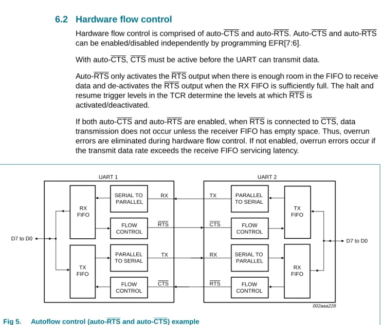
6.2 Hardware flow control
Hardware flow control is comprised of auto-CTS and auto-RTS. Auto-CTS and auto-RTS
can be enabled/disabled independently by programming EFR[7:6].
With auto-CTS, CTS must be active before the UART can transmit data.
Auto-RTS only activates the RTS output when there is enough room in the FIFO to receive
data and de-activates the RTS output when the RX FIFO is sufficiently full. The halt and
resume trigger levels in the TCR determine the levels at which RTS is
activated/deactivated.
If both auto-CTS and auto-RTS are enabled, when RTS is connected to CTS, data
transmission does not occur unless the receiver FIFO has empty space. Thus, overrun
errors are eliminated during hardware flow control. If not enabled, overrun errors occur if
the transmit data rate exceeds the receive FIFO servicing latency.
Fig 5. Autoflow control (auto-RTS and auto-CTS) example
RX FIFO FLOW CONTROL TX FIFO PARALLEL TO SERIAL TX FIFO RX FIFO UART 1 UART 2 D7 to D0 RX TX RTS CTS TX RX CTS RTS D7 to D0 002aaa228 SERIAL TO PARALLEL SERIAL TO PARALLEL FLOW CONTROL FLOW CONTROL FLOW CONTROL PARALLEL TO SERIAL
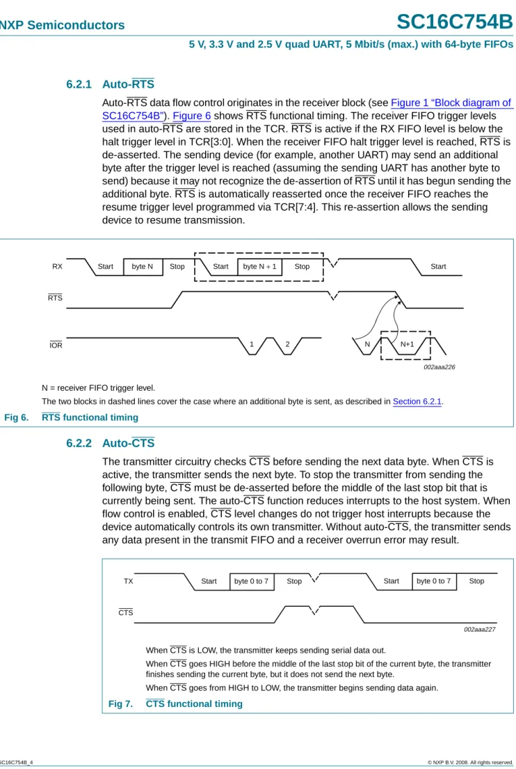
6.2.1 Auto-RTS
Auto-RTS data flow control originates in the receiver block (see
Figure 1 “Block diagram of
SC16C754B”
).
Figure 6
shows RTS functional timing. The receiver FIFO trigger levels
used in auto-RTS are stored in the TCR. RTS is active if the RX FIFO level is below the
halt trigger level in TCR[3:0]. When the receiver FIFO halt trigger level is reached, RTS is
de-asserted. The sending device (for example, another UART) may send an additional
byte after the trigger level is reached (assuming the sending UART has another byte to
send) because it may not recognize the de-assertion of RTS until it has begun sending the
additional byte. RTS is automatically reasserted once the receiver FIFO reaches the
resume trigger level programmed via TCR[7:4]. This re-assertion allows the sending
device to resume transmission.
6.2.2 Auto-CTS
The transmitter circuitry checks CTS before sending the next data byte. When CTS is
active, the transmitter sends the next byte. To stop the transmitter from sending the
following byte, CTS must be de-asserted before the middle of the last stop bit that is
currently being sent. The auto-CTS function reduces interrupts to the host system. When
flow control is enabled, CTS level changes do not trigger host interrupts because the
device automatically controls its own transmitter. Without auto-CTS, the transmitter sends
any data present in the transmit FIFO and a receiver overrun error may result.
N = receiver FIFO trigger level.
The two blocks in dashed lines cover the case where an additional byte is sent, as described inSection 6.2.1.
Fig 6. RTS functional timing
Start byte N Stop Start byte N + 1 Stop Start RX
RTS
IOR 1 2 N N+1
002aaa226
When CTS is LOW, the transmitter keeps sending serial data out.
When CTS goes HIGH before the middle of the last stop bit of the current byte, the transmitter finishes sending the current byte, but it does not send the next byte.
When CTS goes from HIGH to LOW, the transmitter begins sending data again.
Fig 7. CTS functional timing
Start byte 0 to 7 Stop TX
CTS
002aaa227
6.3 Software flow control
Software flow control is enabled through the enhanced feature register and the modem
control register. Different combinations of software flow control can be enabled by setting
different combinations of EFR[3:0].
Table 3
shows software flow control options.
Remark: When using software flow control, the Xon/Xoff characters cannot be used for
data characters.
There are two other enhanced features relating to software flow control:
•
‘Xon Any’ function (MCR[5]): Operation will resume after receiving any character
after recognizing the Xoff character. It is possible that an Xon1 character is
recognized as an ‘Xon Any’ character, which could cause an Xon2 character to be
written to the RX FIFO.
•
Special character (EFR[5]): Incoming data is compared to Xoff2. Detection of the
special character sets the Xoff interrupt (IIR[4]) but does not halt transmission. The
Xoff interrupt is cleared by a read of the IIR. The special character is transferred to the
RX FIFO.
6.3.1 RX
When software flow control operation is enabled, the SC16C754B will compare incoming
data with Xoff1/Xoff2 programmed characters (in certain cases, Xoff1 and Xoff2 must be
received sequentially). When the correct Xoff character is received, transmission is halted
after completing transmission of the current character. Xoff detection also sets IIR[4] (if
enabled via IER[5]) and causes INT to go HIGH.
To resume transmission, an Xon1/Xon2 character must be received (in certain cases
Xon1 and Xon2 must be received sequentially). When the correct Xon characters are
received, IIR[4] is cleared, and the Xoff interrupt disappears.
Table 3. Software flow control options (EFR[3:0])
EFR[3] EFR[2] EFR[1] EFR[0] TX, RX software flow controls
0 0 X X no transmit flow control 1 0 X X transmit Xon1, Xoff1 0 1 X X transmit Xon2, Xoff2
1 1 X X transmit Xon1, Xon2, Xoff1, Xoff2 X X 0 0 no receive flow control
X X 1 0 receiver compares Xon1, Xoff1 X X 0 1 receiver compares Xon2, Xoff2 1 0 1 1 transmit Xon1, Xoff1
receiver compares Xon1 or Xon2, Xoff1 or Xoff2 0 1 1 1 transmit Xon2, Xoff2
receiver compares Xon1 or Xon2, Xoff1 or Xoff2 1 1 1 1 transmit Xon1, Xon2, Xoff1, Xoff2
receiver compares Xon1 and Xon2, Xoff1 and Xoff2 0 0 1 1 no transmit flow control
6.3.2 TX
Xoff1/Xoff2 character is transmitted when the RX FIFO has passed the halt trigger level
programmed in TCR[3:0].
Xon1/Xon2 character is transmitted when the RX FIFO reaches the resume trigger level
programmed in TCR[7:4].
The transmission of Xoff/Xon(s) follows the exact same protocol as transmission of an
ordinary byte from the FIFO. This means that even if the word length is set to be 5, 6, or 7
characters, then the 5, 6, or 7 least significant bits of Xoff1/Xoff2 and Xon1/Xon2 will be
transmitted. (Note that the transmission of 5, 6, or 7 bits of a character is seldom done, but
this functionality is included to maintain compatibility with earlier designs.)
It is assumed that software flow control and hardware flow control will never be enabled
simultaneously.
Figure 8
shows an example of software flow control.
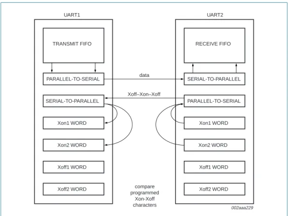
6.3.3 Software flow control example
6.3.3.1
Assumptions
UART1 is transmitting a large text file to UART2. Both UARTs are using software flow
control with single character Xoff (0Fh) and Xon (0Dh) tokens. Both have Xoff threshold
(TCR[3:0] = F) set to 60, and Xon threshold (TCR[7:4] = 8) set to 32. Both have the
interrupt receive threshold (TLR[7:4] = D) set to 52.
Fig 8. Software flow control example TRANSMIT FIFO PARALLEL-TO-SERIAL SERIAL-TO-PARALLEL Xon1 WORD Xon2 WORD Xoff1 WORD Xoff2 WORD RECEIVE FIFO PARALLEL-TO-SERIAL SERIAL-TO-PARALLEL Xon1 WORD Xon2 WORD Xoff1 WORD Xoff2 WORD UART2 UART1 002aaa229 data Xoff–Xon–Xoff compare programmed Xon-Xoff characters
UART1 begins transmission and sends 52 characters, at which point UART2 will generate
an interrupt to its processor to service the RX FIFO, but assumes the interrupt latency is
fairly long. UART1 will continue sending characters until a total of 60 characters have
been sent. At this time, UART2 will transmit a 0Fh to UART1, informing UART1 to halt
transmission. UART1 will likely send the 61
stcharacter while UART2 is sending the Xoff
character. Now UART2 is serviced and the processor reads enough data out of the RX
FIFO that the level drops to 32. UART2 will now send a 0Dh to UART1, informing UART1
to resume transmission.
6.4 Reset
Table 4
summarizes the state of register after reset.
Remark: Registers DLL, DLM, SPR, Xon1, Xon2, Xoff1, Xoff2 are not reset by the
top-level reset signal RESET, that is, they hold their initialization values during reset.
Table 5
summarizes the state of registers after reset.
Table 4. Register reset functionsRegister Reset control Reset state
Interrupt enable register RESET all bits cleared
Interrupt identification register RESET bit 0 is set; all other bits cleared FIFO control register RESET all bits cleared
Line control register RESET reset to 0001 1101 (1Dh) Modem control register RESET all bits cleared
Line status register RESET bit 5 and bit 6 set; all other bits cleared Modem status register RESET bits 3:0 cleared; bits 7:4 input signals Enhanced feature register RESET all bits cleared
Receiver holding register RESET pointer logic cleared Transmitter holding register RESET pointer logic cleared Transmission control register RESET all bits cleared Trigger level register RESET all bits cleared
Table 5. Signal RESET functions
Signal Reset control Reset state
TX RESET HIGH
RTS RESET HIGH
DTR RESET HIGH
RXRDY RESET HIGH
6.5 Interrupts
The SC16C754B has interrupt generation and prioritization (six prioritized levels of
interrupts) capability. The Interrupt Enable Register (IER) enables each of the six types of
interrupts and the INT signal in response to an interrupt generation. The IER can also
disable the interrupt system by clearing bits 7:5 and 3:0. When an interrupt is generated,
the IIR indicates that an interrupt is pending and provides the type of interrupt through
IIR[5:0].
Table 6
summarizes the interrupt control functions.
It is important to note that for the framing error, parity error, and break conditions, LSR[7]
generates the interrupt. LSR[7] is set when there is an error anywhere in the RX FIFO,
and is cleared only when there are no more errors remaining in the FIFO. LSR[4:2] always
represent the error status for the received character at the top of the RX FIFO. Reading
the RX FIFO updates LSR[4:2] to the appropriate status for the new character at the top of
the FIFO. If the RX FIFO is empty, then LSR[4:2] are all zeros.
For the Xoff interrupt, if an Xoff flow character detection caused the interrupt, the interrupt
is cleared by an Xon flow character detection. If a special character detection caused the
interrupt, the interrupt is cleared by a read of the IIR.
Table 6. Interrupt control functions
IIR[5:0] Priority level
Interrupt type Interrupt source Interrupt reset method
00 0001 None none none none
00 0110 1 receiver line status OE, FE, PE, or BI errors occur in characters in the RX FIFO
FE, PE, BI: all erroneous characters are read from the RX FIFO.
OE: read LSR 00 1100 2 RX time-out stale data in RX FIFO read RHR 00 0100 2 RHR interrupt DRDY (data ready)
(FIFO disable)
RX FIFO above trigger level (FIFO enable)
read RHR
00 0010 3 THR interrupt TFE (THR empty) (FIFO disable)
TX FIFO passes above trigger level (FIFO enable)
read IIR or a write to the THR
00 0000 4 modem status MSR[3:0] = 0 read MSR 01 0000 5 Xoff interrupt receive Xoff character(s)/special
character
receive Xon character(s)/Read of IIR
10 0000 6 CTS, RTS RTS pin or CTS pin change state from active (LOW) to inactive (HIGH)
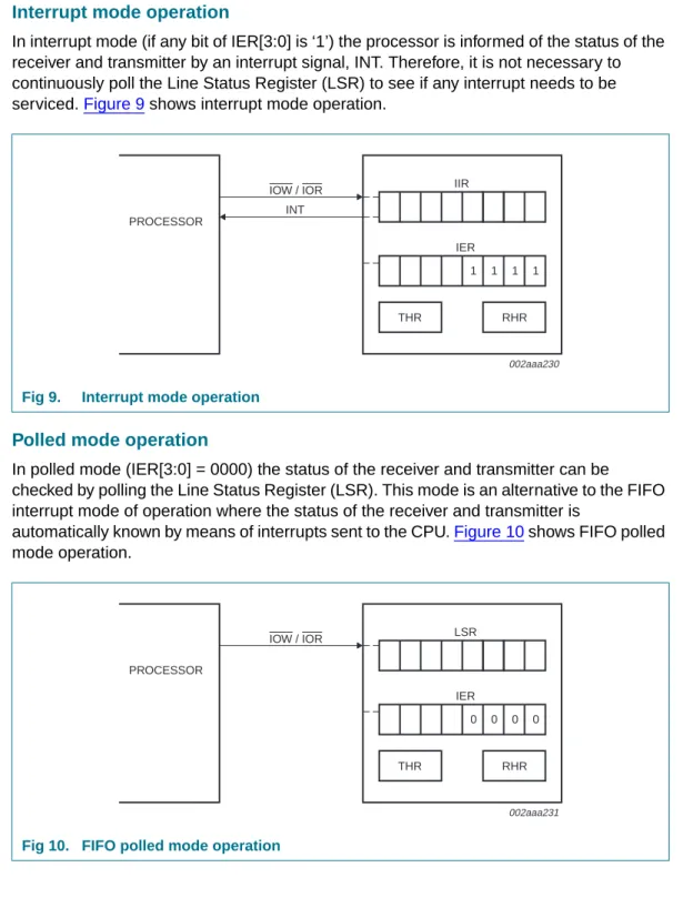
6.5.1 Interrupt mode operation
In interrupt mode (if any bit of IER[3:0] is ‘1’) the processor is informed of the status of the
receiver and transmitter by an interrupt signal, INT. Therefore, it is not necessary to
continuously poll the Line Status Register (LSR) to see if any interrupt needs to be
serviced.
Figure 9
shows interrupt mode operation.
6.5.2 Polled mode operation
In polled mode (IER[3:0] = 0000) the status of the receiver and transmitter can be
checked by polling the Line Status Register (LSR). This mode is an alternative to the FIFO
interrupt mode of operation where the status of the receiver and transmitter is
automatically known by means of interrupts sent to the CPU.
Figure 10
shows FIFO polled
mode operation.
Fig 9. Interrupt mode operation
1 1 1 1 IIR IER THR RHR PROCESSOR IOW / IOR INT 002aaa230
Fig 10. FIFO polled mode operation
0 0 0 0 LSR IER THR RHR PROCESSOR IOW / IOR 002aaa231
6.6 DMA operation
There are two modes of DMA operation, DMA mode 0 or DMA mode 1, selected by
FCR[3].
In DMA mode 0 or FIFO disable (FCR[0] = 0) DMA occurs in single character transfers. In
DMA mode 1, multi-character (or block) DMA transfers are managed to relieve the
processor for longer periods of time.
6.6.1 Single DMA transfers (DMA mode 0/FIFO disable)
Figure 11
shows TXRDY and RXRDY in DMA mode 0/FIFO disable.
6.6.1.1
Transmitter
When empty, the TXRDY signal becomes active. TXRDY will go inactive after one
character has been loaded into it.
6.6.1.2
Receiver
RXRDY is active when there is at least one character in the FIFO. It becomes inactive
when the receiver is empty.
Fig 11. TXRDY and RXRDY in DMA mode 0/FIFO disable TX wrptr wrptr FIFO EMPTY TXRDY RX rdptr rdptr FIFO EMPTY RXRDY RXRDY 002aaa232 at least one location filled at least one location filled TXRDY
6.6.2 Block DMA transfers (DMA mode 1)
Figure 12
shows TXRDY and RXRDY in DMA mode 1.
6.6.2.1
Transmitter
TXRDY is active when there is a trigger level number of spaces available. It becomes
inactive when the FIFO is full.
6.6.2.2
Receiver
RXRDY becomes active when the trigger level has been reached, or when a time-out
interrupt occurs. It will go inactive when the FIFO is empty or an error in the RX FIFO is
flagged by LSR[7].
6.7 Sleep mode
Sleep mode is an enhanced feature of the SC16C754B UART. It is enabled when EFR[4],
the enhanced functions bit, is set and when IER[4] is set. Sleep mode is entered when:
•
The serial data input line, RX, is idle (see
Section 6.8 “Break and time-out
conditions”
).
•
The TX FIFO and TX shift register are empty.
•
There are no interrupts pending except THR and time-out interrupts.
Remark: Sleep mode will not be entered if there is data in the RX FIFO.
In Sleep mode, the UART clock and baud rate clock are stopped. Since most registers are
clocked using these clocks, the power consumption is greatly reduced. The UART will
wake up when any change is detected on the RX line, when there is any change in the
state of the modem input pins, or if data is written to the TX FIFO.
Remark: Writing to the divisor latches, DLL and DLM, to set the baud clock, must not be
done during Sleep mode. Therefore, it is advisable to disable Sleep mode using IER[4]
before writing to DLL or DLM.
Fig 12. TXRDY and RXRDY in DMA mode 1
TX wrptr wrptr TXRDY FIFO full TXRDY RX rdptr rdptr FIFO EMPTY RXRDY RXRDY 002aaa869 trigger level trigger level
6.8 Break and time-out conditions
An RX idle condition is detected when the receiver line, RX, has been HIGH for
4 character time. The receiver line is sampled midway through each bit.
When a break condition occurs, the TX line is pulled LOW. A break condition is activated
by setting LCR[6].
6.9 Programmable baud rate generator
The SC16C754B UART contains a programmable baud generator that takes any clock
input and divides it by a divisor in the range between 1 and (2
16−
1). An additional
divide-by-4 prescaler is also available and can be selected by MCR[7], as shown in
Figure 13
. The output frequency of the baud rate generator is 16
× the baud rate. The
formula for the divisor is given in
Equation 1
:
(1)
Where:
prescaler = 1, when MCR[7] is set to 0 after reset (divide-by-1 clock selected)
prescaler = 4, when MCR[7] is set to 1 after reset (divide-by-4 clock selected).
Remark: The default value of prescaler after reset is divide-by-1.
Figure 13
shows the internal prescaler and baud rate generator circuitry.
DLL and DLM must be written to in order to program the baud rate. DLL and DLM are the
least significant and most significant byte of the baud rate divisor. If DLL and DLM are
both zero, the UART is effectively disabled, as no baud clock will be generated.
Remark: The programmable baud rate generator is provided to select both the transmit
and receive clock rates.
Table 7
and
Table 8
show the baud rate and divisor correlation for crystal with frequency
1.8432 MHz and 3.072 MHz, respectively.
Figure 14
shows the crystal clock circuit reference.
Fig 13. Prescaler and baud rate generator block diagramdivisor
XTAL1 crystal input frequency
prescaler
---
desired baud rate
×
16
(
)
---=
BAUD RATE GENERATOR LOGIC MCR[7] = 1 MCR[7] = 0 PRESCALER LOGIC (DIVIDE-BY-1) INTERNAL OSCILLATOR LOGIC 002aaa233 XTAL1 XTAL2 input clock PRESCALER LOGIC (DIVIDE-BY-4) reference clock internal baud rate clock for transmitter and receiverTable 7. Baud rates using a 1.8432 MHz crystal
Desired baud rate Divisor used to generate 16×clock
Percent error difference between desired and actual
50 2304 75 1536 110 1047 0.026 134.5 857 0.058 150 768 300 384 600 192 1200 96 1800 64 2000 58 0.69 2400 48 3600 32 4800 24 7200 16 9600 12 19200 6 38400 3 56000 2 2.86
Table 8. Baud rates using a 3.072 MHz crystal
Desired baud rate Divisor used to generate 16×clock
Percent error difference between desired and actual
50 3840 75 2560 110 1745 0.026 134.5 1428 0.034 150 1280 300 640 600 320 1200 160 1800 107 0.312 2000 96 2400 80 3600 53 0.628 4800 40 7200 27 1.23 9600 20 19200 10 38400 5
7.
Register descriptions
Each register is selected using address lines A0, A1, A2, and in some cases, bits from
other registers. The programming combinations for register selection are shown in
Table 9
.
[1] MCR[7] can only be modified when EFR[4] is set.
[2] Accessed by a combination of address pins and register bits. [3] Accessible only when LCR[7] is logic 1.
[4] Accessible only when LCR is set to 1011 1111 (BFh).
Fig 14. Crystal oscillator connection
002aaa870 C2 47 pF XTAL1 XTAL2 X1 1.8432 MHz C1 22 pF C2 33 pF XTAL1 XTAL2 1.5 kΩ X1 1.8432 MHz C1 22 pF
Table 9. Register map - read/write properties
A2 A1 A0 Read mode Write mode
0 0 0 Receive Holding Register (RHR) Transmit Holding Register (THR) 0 0 1 Interrupt Enable Register (IER) Interrupt Enable Register (IER) 0 1 0 Interrupt Identification Register (IIR) FIFO Control Register (FCR) 0 1 1 Line Control Register (LCR) Line Control Register (LCR) 1 0 0 Modem Control Register (MCR)[1] Modem Control Register (MCR)[1]
1 0 1 Line Status Register (LSR) not applicable 1 1 0 Modem Status Register (MSR) not applicable
1 1 1 ScratchPad Register (SPR) ScratchPad Register (SPR) 0 0 0 Divisor Latch LSB (DLL)[2][3] Divisor Latch LSB (DLL)[2][3]
0 0 1 Divisor Latch MSB (DLM)[2][3] Divisor Latch MSB (DLM)[2][3]
0 1 0 Enhanced Feature Register (EFR)[2][4] Enhanced Feature Register (EFR)[2][4]
1 0 0 Xon1 word[2][4] Xon1 word[2][4]
1 0 1 Xon2 word[2][4] Xon2 word[2][4]
1 1 0 Xoff1 word[2][4] Xoff1 word[2][4]
1 1 1 Xoff2 word[2][4] Xoff2 word[2][4]
1 1 0 Transmission Control Register (TCR)[2][5]
Transmission Control Register (TCR)[2][5]
1 1 1 Trigger Level Register (TLR)[2][5] Trigger Level Register (TLR)[2][5]
Table 10
lists and describes the SC16C754B internal registers.
[1] These registers are accessible only when LCR[7] = 0.
[2] This bit can only be modified if register bit EFR[4] is enabled, that is, if enhanced functions are enabled. [3] The Special register set is accessible only when LCR[7] is set to a logic 1.
Table 10. SC16C754B internal registers
A2 A1 A0 Register Bit 7 Bit 6 Bit 5 Bit 4 Bit 3 Bit 2 Bit 1 Bit 0 Read/ Write
General register set[1]
0 0 0 RHR bit 7 bit 6 bit 5 bit 4 bit 3 bit 2 bit 1 bit 0 R 0 0 0 THR bit 7 bit 6 bit 5 bit 4 bit 3 bit 2 bit 1 bit 0 W 0 0 1 IER 0/CTS interrupt enable[2] 0/RTS interrupt enable[2] 0/Xoff[2] 0/X Sleep mode[2] modem status interrupt receive line status interrupt THR empty interrupt RX data available interrupt R/W 0 1 0 FCR RX trigger level (MSB) RX trigger level (LSB) 0/TX trigger level (MSB)[2] 0/TX trigger level (LSB)[2] DMA mode select TX FIFO reset RX FIFO reset FIFO enable W 0 1 0 IIR FCR[0] FCR[0] 0/CTS, RTS 0/Xoff interrupt priority bit 2 interrupt priority bit 1 interrupt priority bit 0 interrupt status R 0 1 1 LCR DLAB break control bit
set parity parity type select parity enable number of stop bits word length bit 1 word length bit 0 R/W 1 0 0 MCR 1× or 1×/ 4 clock[2] TCR and TLR enable[2] 0/Xon Any [2] 0/enable loopback IRQ enable OP FIFO ready enable RTS DTR R/W 1 0 1 LSR 0/error in RX FIFO THR and TSR empty THR empty break interrupt framing error
parity error overrun error
data in receiver
R
1 1 0 MSR CD RI DSR CTS ∆CD ∆RI ∆DSR ∆CTS R 1 1 1 SPR bit 7 bit 6 bit 5 bit 4 bit 3 bit 2 bit 1 bit 0 R/W 1 1 0 TCR bit 7 bit 6 bit 5 bit 4 bit 3 bit 2 bit 1 bit 0 R/W 1 1 1 TLR bit 7 bit 6 bit 5 bit 4 bit 3 bit 2 bit 1 bit 0 R/W 1 1 1 FIFO Rdy RX FIFO D status RX FIFO C status RX FIFO B status RX FIFO A status TX FIFO D status TX FIFO C status TX FIFO B status TX FIFO A status R
Special register set[3]
0 0 0 DLL bit 7 bit 6 bit 5 bit 4 bit 3 bit 2 bit 1 bit 0 R/W 0 0 1 DLM bit 15 bit 14 bit 13 bit 12 bit 11 bit 10 bit 9 bit 8 R/W
Enhanced register set[4]
0 1 0 EFR auto-CTS auto-RTS special character detect enable enhanced functions [2] software flow control bit 3 software flow control bit 2 software flow control bit 1 software flow control bit 0 R/W
1 0 0 Xon1 bit 7 bit 6 bit 5 bit 4 bit 3 bit 2 bit 1 bit 0 R/W 1 0 1 Xon2 bit 7 bit 6 bit 5 bit 4 bit 3 bit 2 bit 1 bit 0 R/W 1 1 0 Xoff1 bit 7 bit 6 bit 5 bit 4 bit 3 bit 2 bit 1 bit 0 R/W 1 1 1 Xoff2 bit 7 bit 6 bit 5 bit 4 bit 3 bit 2 bit 1 bit 0 R/W
Remark: Refer to the notes under
Table 9
for more register access information.
7.1 Receiver Holding Register (RHR)
The receiver section consists of the Receiver Holding Register (RHR) and the Receiver
Shift Register (RSR). The RHR is actually a 64-byte FIFO. The RSR receives serial data
from the RX terminal. The data is converted to parallel data and moved to the RHR. The
receiver section is controlled by the Line Control Register (LCR). If the FIFO is disabled,
location zero of the FIFO is used to store the characters.
Remark: In this case, characters are overwritten if overflow occurs.
If overflow occurs, characters are lost. The RHR also stores the error status bits
associated with each character.
7.2 Transmit Holding Register (THR)
The transmitter section consists of the Transmit Holding Register (THR) and the Transmit
Shift Register (TSR). The THR is actually a 64-byte FIFO. The THR receives data and
shifts it into the TSR, where it is converted to serial data and moved out on the TX
terminal. If the FIFO is disabled, the FIFO is still used to store the byte. Characters are
lost if overflow occurs.
7.3 FIFO Control Register (FCR)
This is a write-only register that is used for enabling the FIFOs, clearing the FIFOs, setting
transmitter and receiver trigger levels, and selecting the type of DMA signalling.
Table 11
shows FIFO control register bit settings.
Table 11. FIFO control register bits descriptionBit Symbol Description
7:6 FCR[7] (MSB), FCR[6] (LSB)
RX trigger. Sets the trigger level for the RX FIFO.
00 — 8 characters 01 — 16 characters 10 — 56 characters 11 — 60 characters 5:4 FCR[5] (MSB), FCR[4] (LSB)
TX trigger. Sets the trigger level for the TX FIFO.
00 — 8 spaces 01 — 16 spaces 10 — 32 spaces 11 — 56 spaces
FCR[5:4] can only be modified and enabled when EFR[4] is set. This is because the transmit trigger level is regarded as an enhanced function. 3 FCR[3] DMA mode select.
logic 0 = set DMA mode 0 logic 1 = set DMA mode 1 2 FCR[2] Reset TX FIFO.
logic 0 = no FIFO transmit reset (normal default condition)
logic 1 = clears the contents of the transmit FIFO and resets the FIFO counter logic (the transmit shift register is not cleared or altered). This bit will return to a logic 0 after clearing the FIFO.
1 FCR[1] Reset RX FIFO.
logic 0 = no FIFO receive reset (normal default condition)
logic 1 = clears the contents of the receive FIFO and resets the FIFO counter logic (the receive shift register is not cleared or altered). This bit will return to a logic 0 after clearing the FIFO.
0 FCR[0] FIFO enable.
logic 0 = disable the transmit and receive FIFO (normal default condition)
7.4 Line Control Register (LCR)
This register controls the data communication format. The word length, number of stop
bits, and parity type are selected by writing the appropriate bits to the LCR.
Table 12
shows the line control register bit settings.
Table 12. Line control register bits descriptionBit Symbol Description
7 LCR[7] Divisor latch enable.
logic 0 = divisor latch disabled (normal default condition) logic 1 = divisor latch enabled
6 LCR[6] Break control bit. When enabled, the Break control bit causes a break condition to be transmitted (the TX output is forced to a logic 0 state). This condition exists until disabled by setting LCR[6] to a logic 0.
logic 0 = no TX break condition (normal default condition) logic 1 = forces the transmitter output (TX) to a logic 0 to alert the communication terminal to a line break condition
5 LCR[5] Set parity. LCR[5] selects the forced parity format (if LCR[3] = 1). logic 0 = parity is not forced (normal default condition)
LCR[5] = logic 1 and LCR[4] = logic 0: parity bit is forced to a logic 1 for the transmit and receive data
LCR[5] = logic 1 and LCR[4] = logic 1: parity bit is forced to a logic 0 for the transmit and receive data
4 LCR[4] Parity type select.
logic 0 = odd parity is generated (if LCR[3] = 1) logic 1 = even parity is generated (if LCR[3] = 1) 3 LCR[3] Parity enable.
logic 0 = no parity (normal default condition)
logic 1 = a parity bit is generated during transmission and the receiver checks for received parity
2 LCR[2] Number of stop bits. Specifies the number of stop bits. 0 = 1 stop bit (word length = 5, 6, 7, 8)
1 = 1.5 stop bits (word length = 5) 1 = 2 stop bits (word length = 6, 7, 8)
1:0 LCR[1:0] Word length bits 1, 0. These two bits specify the word length to be transmitted or received.
00 — 5 bits 01 — 6 bits 10 — 7 bits 11 — 8 bits
7.5 Line Status Register (LSR)
Table 13
shows the line status register bit settings.
When the LSR is read, LSR[4:2] reflect the error bits (BI, FE, PE) of the character at the
top of the RX FIFO (next character to be read). The LSR[4:2] registers do not physically
exist, as the data read from the RX FIFO is output directly onto the output data bus,
DI[4:2], when the LSR is read. Therefore, errors in a character are identified by reading
the LSR and then reading the RHR.
LSR[7] is set when there is an error anywhere in the RX FIFO, and is cleared only when
there are no more errors remaining in the FIFO.
Reading the LSR does not cause an increment of the RX FIFO read pointer. The RX FIFO
read pointer is incremented by reading the RHR.
Table 13. Line status register bits description
Bit Symbol Description
7 LSR[7] FIFO data error.
logic 0 = no error (normal default condition)
logic 1 = at least one parity error, framing error, or break indication is in the receiver FIFO. This bit is cleared when no more errors are present in the FIFO.
6 LSR[6] THR and TSR empty. This bit is the Transmit Empty indicator. logic 0 = transmitter hold and shift registers are not empty logic 1 = transmitter hold and shift registers are empty
5 LSR[5] THR empty. This bit is the Transmit Holding Register Empty indicator. logic 0 = Transmit Hold Register is not empty
logic 1 = Transmit Hold Register is empty. The processor can now load up to 64 bytes of data into the THR if the TX FIFO is enabled.
4 LSR[4] Break interrupt.
logic 0 = no break condition (normal default condition)
logic 1 = a break condition occurred and associated byte is 00, that is, RX was LOW for one character time frame
3 LSR[3] Framing error.
logic 0 = no framing error in data being read from RX FIFO (normal default condition)
logic 1 = framing error occurred in data being read from RX FIFO, that is, received data did not have a valid stop bit
2 LSR[2] Parity error.
logic 0 = no parity error (normal default condition) logic 1 = parity error in data being read from RX FIFO 1 LSR[1] Overrun error.
logic 0 = no overrun error (normal default condition) logic 1 = overrun error has occurred
0 LSR[0] Data in receiver.
logic 0 = no data in receive FIFO (normal default condition) logic 1 = at least one character in the RX FIFO
7.6 Modem Control Register (MCR)
The MCR controls the interface with the modem, data set, or peripheral device that is
emulating the modem.
Table 14
shows modem control register bit settings.
[1] MCR[7:5] can only be modified when EFR[4] is set, that is, EFR[4] is a write enable.
Table 14. Modem control register bits description
Bit Symbol Description
7 MCR[7][1] Clock select.
logic 0 = divide-by-1 clock input logic 1 = divide-by-4 clock input 6 MCR[6][1] TCR and TLR enable.
logic 0 = no action
logic 1 = enable access to the TCR and TLR registers 5 MCR[5][1] Xon Any.
logic 0 = disable Xon Any function logic 1 = enable Xon Any function 4 MCR[4] Enable loopback.
logic 0 = normal operating mode
logic 1 = enable local loopback mode (internal). In this mode the MCR[3:0] signals are looped back into MSR[7:4] and the TX output is looped back to the RX input internally.
3 MCR[3] IRQ enable OP.
logic 0 = forces INTA to INTD outputs to the 3-state mode and OP output to HIGH state
logic 1 = forces the INTA to INTD outputs to the active state and OP output to LOW state. In loopback mode, controls MSR[7].
2 MCR[2] FIFO Ready enable.
logic 0 = disable the FIFO Rdy register
logic 1 = enable the FIFO Rdy register. In loopback mode, controls MSR[6].
1 MCR[1] RTS
logic 0 = force RTS output to inactive (HIGH)
logic 1 = force RTS output to active (LOW). In loopback mode, controls MSR[4]. If auto-RTS is enabled, the RTS output is controlled by hardware flow control.
0 MCR[0] DTR
logic 0 = force DTR output to inactive (HIGH)
logic 1 = force DTR output to active (LOW). In loopback mode, controls MSR[5].
7.7 Modem Status Register (MSR)
This 8-bit register provides information about the current state of the control lines from the
modem, data set, or peripheral device to the processor. It also indicates when a control
input from the modem changes state.
Table 15
shows modem status register bit settings
per channel.
[1] The primary inputs RI, CD, CTS, DSR are all active LOW, but their registered equivalents in the MSR and MCR (in loopback) registers are active HIGH.
Table 15. Modem status register bits description
Bit Symbol Description
7 MSR[7][1] CD (active HIGH, logic 1). This bit is the complement of the CD input during
normal mode. During internal loopback mode, it is equivalent to MCR[3]. 6 MSR[6][1] RI (active HIGH, logic 1). This bit is the complement of the RI input during
normal mode. During internal loopback mode, it is equivalent to MCR[2]. 5 MSR[5][1] DSR (active HIGH, logic 1). This bit is the complement of the DSR input
during normal mode. During internal loopback mode, it is equivalent MCR[0]. 4 MSR[4][1] CTS (active HIGH, logic 1). This bit is the complement of the CTS input
during normal mode. During internal loopback mode, it is equivalent to MCR[1].
3 MSR[3] ∆CD. Indicates that CD input (or MCR[3] in loopback mode) has changed state. Cleared on a read.
2 MSR[2] ∆RI. Indicates that RI input (or MCR[2] in loopback mode) has changed state from LOW to HIGH. Cleared on a read.
1 MSR[1] ∆DSR. Indicates that DSR input (or MCR[0] in loopback mode) has changed state. Cleared on a read.
0 MSR[0] ∆CTS. Indicates that CTS input (or MCR[1] in loopback mode) has changed state. Cleared on a read.
7.8 Interrupt Enable Register (IER)
The Interrupt Enable Register (IER) enables each of the six types of interrupt, receiver
error, RHR interrupt, THR interrupt, Xoff received, or CTS/RTS change of state from LOW
to HIGH. The INT output signal is activated in response to interrupt generation.
Table 16
shows the interrupt enable register bit settings.
[1] IER[7:4] can only be modified if EFR[4] is set, that is, EFR[4] is a write enable. Re-enabling IER[1] will cause a new interrupt if the THR is below the threshold.
Table 16. Interrupt enable register bits description
Bit Symbol Description
7 IER[7][1] CTS interrupt enable.
logic 0 = disable the CTS interrupt (normal default condition) logic 1 = enable the CTS interrupt
6 IER[6][1] RTS interrupt enable.
logic 0 = disable the RTS interrupt (normal default condition) logic 1 = enable the RTS interrupt
5 IER[5][1] Xoff interrupt.
logic 0 = disable the Xoff interrupt (normal default condition) logic 1 = enable the Xoff interrupt
4 IER[4][1] Sleep mode.
logic 0 = disable Sleep mode (normal default condition)
logic 1 = enable Sleep mode. SeeSection 6.7 “Sleep mode” for details. 3 IER[3] Modem status interrupt.
logic 0 = disable the modem status register interrupt (normal default condition)
logic 1 = enable the modem status register interrupt 2 IER[2] Receive line status interrupt.
logic 0 = disable the receiver line status interrupt (normal default condition) logic 1 = enable the receiver line status interrupt
1 IER[1] Transmit holding register interrupt.
logic 0 = disable the THR interrupt (normal default condition) logic 1 = enable the THR interrupt
0 IER[0] Receive holding register interrupt.
logic 0 = disable the RHR interrupt (normal default condition) logic 1 = enable the RHR interrupt
7.9 Interrupt Identification Register (IIR)
The IIR is a read-only 8-bit register which provides the source of the interrupt in a
prioritized manner.
Table 17
shows interrupt identification register bit settings.
The interrupt priority list is shown in
Table 18
.
Table 17. Interrupt identification register bits description
Bit Symbol Description
7:6 IIR[7:6] Mirror the contents of FCR[0].
5 IIR[5] RTS/CTS LOW-to-HIGH change of state. 4 IIR[4] 1 = Xoff/special character has been detected. 3:1 IIR[3:1] 3-bit encoded interrupt. SeeTable 18. 0 IIR[0] Interrupt status.
logic 0 = an interrupt is pending logic 1 = no interrupt is pending
Table 18. Interrupt priority list
Priority level
IIR[5] IIR[4] IIR[3] IIR[2] IIR[1] IIR[0] Source of the interrupt
1 0 0 0 1 1 0 Receiver line status error 2 0 0 1 1 0 0 Receiver time-out interrupt
2 0 0 0 1 0 0 RHR interrupt
3 0 0 0 0 1 0 THR interrupt
4 0 0 0 0 0 0 Modem interrupt
5 0 1 0 0 0 0 Received Xoff signal/ special character
6 1 0 0 0 0 0 CTS, RTS change of state from active (LOW) to inactive (HIGH)
7.10 Enhanced Feature Register (EFR)
This 8-bit register enables or disables the enhanced features of the UART.
Table 19
shows
the enhanced feature register bit settings.
7.11 Divisor latches (DLL, DLM)
These are two 8-bit registers which store the 16-bit divisor for generation of the baud clock
in the baud rate generator. DLM stores the most significant part of the divisor. DLL stores
the least significant part of the divisor.
Note that DLL and DLM can only be written to before Sleep mode is enabled, that is,
before IER[4] is set.
Table 19. Enhanced feature register bits description
Bit Symbol Description
7 EFR[7] CTS flow control enable.
logic 0 = CTS flow control is disabled (normal default condition)
logic 1 = CTS flow control is enabled. Transmission will stop when a HIGH signal is detected on the CTS pin.
6 EFR[6] RTS flow control enable.
logic 0 = RTS flow control is disabled (normal default condition)
logic 1 = RTS flow control is enabled. The RTS pin goes HIGH when the receiver FIFO HALT trigger level TCR[3:0] is reached, and goes LOW when the receiver FIFO RESUME transmission trigger level TCR[7:4] is reached. 5 EFR[5] Special character detect.
logic 0 = special character detect disabled (normal default condition) logic 1 = special character detect enabled. Received data is compared with Xoff2 data. If a match occurs, the received data is transferred to FIFO and IIR[4] is set to a logic 1 to indicate a special character has been detected. 4 EFR[4] Enhanced functions enable bit.
logic 0 = disables enhanced functions and writing to IER[7:4], FCR[5:4], MCR[7:5].
logic 1 = enables the enhanced function IER[7:4], FCR[5:4], and MCR[7:5] can be modified, that is, this bit is therefore a write enable.
3:0 EFR[3:0] Combinations of software flow control can be selected by programming these bits. SeeTable 3 “Software flow control options (EFR[3:0])”.
7.12 Transmission Control Register (TCR)
This 8-bit register is used to store the RX FIFO threshold levels to stop/start transmission
during hardware/software flow control.
Table 20
shows transmission control register bit
settings.
TCR trigger levels are available from 0 to 60 bytes with a granularity of four.
Remark: TCR can only be written to when EFR[4] = 1 and MCR[6] = 1. The programmer
must program the TCR such that TCR[3:0] > TCR[7:4]. There is no built-in hardware
check to make sure this condition is met. Also, the TCR must be programmed with this
condition before auto-RTS or software flow control is enabled to avoid spurious operation
of the device.
7.13 Trigger Level Register (TLR)
This 8-bit register is used to store the transmit and received FIFO trigger levels used for
DMA and interrupt generation. Trigger levels from 4 to 60 can be programmed with a
granularity of 4.
Table 21
shows trigger level register bit settings.
Remark: TLR can only be written to when EFR[4] = 1 and MCR[6] = 1. If TLR[3:0] or
TLR[7:4] are logic 0, the selectable trigger levels via the FIFO Control Register (FCR) are
used for the transmit and receive FIFO trigger levels. Trigger levels from 4 to 60 bytes are
available with a granularity of four. The TLR should be programmed for
N⁄
4
, where N is the
desired trigger level.
7.14 FIFO Ready register (FIFO Rdy)
The FIFO Rdy register provides real-time status of the transmit and receive FIFOs of both
channels.
Table 20. Transmission control register bits description
Bit Symbol Description
7:4 TCR[7:4] RX FIFO trigger level to resume transmission [(0 to 60) bytes]. 3:0 TCR[3:0] RX FIFO trigger level to halt transmission [(0 to 60) bytes].
Table 21. Trigger level register bits description
Bit Symbol Description
7:4 TLR[7:4] RX FIFO trigger levels (4 to 60), number of characters available. 3:0 TLR[3:0] TX FIFO trigger levels (4 to 60), number of spaces available.
Table 22. FIFO ready register bits description
Bit Symbol Description
7:4 FIFO Rdy[7:4] 0 = there are less than a RX trigger level number of characters in the RX FIFO
1 = the RX FIFO has more than a RX trigger level number of characters available for reading or a time-out condition has occurred
3:0 FIFO Rdy[3:0] 0 = there are less than a TX trigger level number of spaces available in the TX FIFO
1 = there are at least a TX trigger level number of spaces available in the TX FIFO
The FIFO ready register is a read-only register that can be accessed when any of the four
UARTs is selected CSA to CSD = 0, MCR[2] (FIFO Rdy Enable) is a logic 1, and loopback
is disabled. The address is 111.
8.
Programmer’s guide
The base set of registers that is used during high-speed data transfer have a
straightforward access method. The extended function registers require special access
bits to be decoded along with the address lines. The following guide will help with
programming these registers. Note that the descriptions below are for individual register
access. Some streamlining through interleaving can be obtained when programming all
the registers.
Table 23. Register programming guide
Command Actions
set baud rate to VALUE1, VALUE2 read LCR (03h), save in temp set LCR (03h) to 80h
set DLL (00h) to VALUE1 set DLM (01h) to VALUE2 set LCR (03h) to temp set Xoff1, Xon1 to VALUE1, VALUE2 read LCR (03h), save in temp
set LCR (03h) to BFh set Xoff1 (06h) to VALUE1 set Xon1 (04h) to VALUE2 set LCR (03h) to temp set Xoff2, Xon2 to VALUE1, VALUE2 read LCR (03h), save in temp
set LCR (03h) to BFh set Xoff2 (07h) to VALUE1 set Xon2 (05h) to VALUE2 set LCR (03h) to temp set software flow control mode to VALUE read LCR (03h), save in temp
set LCR (03h) to BFh set EFR (02h) to VALUE set LCR (03h) to temp
set flow control threshold to VALUE read LCR (03h), save in temp1 set LCR (03h) to BFh
read EFR (02h), save in temp2 set EFR (02h) to 10h + temp2 set LCR (03h) to 00h
read MCR (04h), save in temp3 set MCR (04h) to 40h + temp3 set TCR (06h) to VALUE set MCR (04h) to temp3 set LCR (03h) to BFh set EFR (02h) to temp2
[1] × sign here means bit-AND.
set TX FIFO and RX FIFO thresholds to VALUE
read LCR (03h), save in temp1 set LCR (03h) to BFh
read EFR (02h), save in temp2 set EFR (02h) to 10h + temp2 set LCR (03h) to 00h
read MCR (04h), save in temp3 set MCR (04h) to 40h + temp3 set TLR (07h) to VALUE set MCR (04h) to temp3 set LCR (03h) to BFh set EFR (02h) to temp2 set LCR (03h) to temp1 read FIFO Rdy register read MCR (04h), save in temp1
set temp2 = temp1× EFh[1]
set MCR (04h) = 40h + temp2 read FFR (07h), save in temp2 pass temp2 back to host set MCR (04h) to temp1 set prescaler value to divide-by-1 read LCR (03h), save in temp1
set LCR (03h) to BFh
read EFR (02h), save in temp2 set EFR (02h) to 10h + temp2 set LCR (03h) to 00h
read MCR (04h), save in temp3 set MCR (04h) to temp3× 7Fh[1]
set LCR (03h) to BFh set EFR (02h) to temp2 set LCR (03h) to temp1 set prescaler value to divide-by-4 read LCR (03h), save in temp1
set LCR (03h) to BF
read EFR (02h), save in temp2 set EFR (02h) to 10h + temp2 set LCR (03h) to 00h
read MCR (04)h, save in temp3 set MCR (04h) to temp3 + 80h set LCR (03)h to BFh
set EFR (02h) to temp2 set LCR (03h) to temp1
Table 23. Register programming guide …continued
9.
Limiting values
Table 24. Limiting values
In accordance with the Absolute Maximum Rating System (IEC 60134).
Symbol Parameter Conditions Min Max Unit
VCC supply voltage - 7 V
Vn voltage on any other pin at D7 to D0 GND−0.3 VCC+ 0.3 V at any input only pin GND−0.3 5.3 V Tamb ambient temperature operating in free-air −40 +85 °C Tstg storage temperature −65 +150 °C
10. Static characteristics
[1] Meets TTL levels, Vio(min)= 2 V and VIH(max)= 0.8 V on non-hysteresis inputs. [2] Applies for external output buffers.
[3] These parameters apply for D7 to D0.
[4] These parameters apply for DTRA, DTRB, INIA, INTB, RTSA, RTSB, RXRDYA, RXRDYB, TXRDYA, TXRDYB, TXA, TXB.
[5] Except XTAL2, VOL= 1 V typical.
[6] These junction temperatures reflect simulated conditions. Absolute maximum junction temperature is 150°C. The customer is responsible for verifying junction temperature.
[7] Applies to external clock; crystal oscillator max. 24 MHz.
[8] Measurement condition, normal operation other than Sleep mode:
VCC= 3.3 V; Tamb= 25°C. Full duplex serial activity on all two serial (UART) channels at the clock frequency specified in the recommended operating conditions with divisor of 1.
[9] When using crystal oscillator. The use of an external clock will increase the sleep current.
Table 25. Static characteristics
Tolerance of VCC±10 %, unless otherwise specified.
Symbol Parameter Conditions VCC= 2.5 V VCC= 3.3 V and 5 V Unit
Min Typ Max Min Typ Max
VCC supply voltage VCC−10 % VCC VCC+ 10 % VCC−10 % VCC VCC+ 10 % V VI input voltage 0 - VCC 0 - VCC V VIH HIGH-level input voltage [1] 1.6 - V CC 2.0 - VCC V VIL LOW-level input voltage [1] - - 0.65 - - 0.8 V VO output voltage [2] 0 - VCC 0 - VCC V VOH HIGH-level output voltage IOH=−8 mA [3] - - - 2.0 - - V IOH=−4 mA [4] - - - 2.0 - - V IOH=−800µA [3] 1.85 - - - V IOH=−400µA [4] 1.85 - - - V VOL LOW-level output voltage[5] IOL= 8 mA [3] - - - 0.4 V IOL= 4 mA [4] - - - 0.4 V IOL= 2 mA [3] - - 0.4 - - - V IOL= 1.6 mA [4] - - 0.4 - - - V Ci input capacitance - - 18 - - 18 pF Tamb ambient temperature operating in free air −40 +25 +85 −40 +25 +85 °C Tj junction temperature [6] 0 25 125 0 25 125 °C
f(i)XTAL1 crystal input frequency
[7] - - 50 - - 80 MHz
δ clock duty cycle - 50 - - 50 - %
ICC supply current f = 5 MHz [8] - - 4.5 - - 6 mA ICC(sleep) sleep mode
supply current
11. Dynamic characteristics
Table 26. Dynamic characteristics
Tamb=−40°C to +85°C; tolerance of VCC±10 %, unless otherwise specified.
Symbol Parameter Conditions VCC= 2.5 V VCC= 3.3 V VCC= 5.0 V Unit
Min Max Min Max Min Max
tWL pulse width LOW 10 - 6 - 6 - ns
tWH pulse width HIGH 10 - 6 - 6 - ns
fXTAL oscillator/clock frequency [1][2] - 48 - 80 80 MHz
t6s address set-up time 0 - 0 - 0 - ns
t6h address hold time 0 - 0 - 0 - ns
t7d IOR delay from chip select 10 - 10 - 10 - ns t7w IOR strobe width 25 pF load 90 - 26 - 23 - ns t7h chip select hold time from IOR 0 - 0 - 0 - ns t9d read cycle delay 25 pF load 20 - 20 - 20 - ns t12d delay from IOR to data 25 pF load - 90 - 26 - 23 ns t12h data disable time 25 pF load - 15 - 15 - 15 ns t13d IOW delay from chip select 10 - 10 - 10 - ns
t13w IOW strobe width 20 - 20 - 15 - ns
t13h chip select hold time from IOW 0 - 0 - 0 - ns
t15d write cycle delay 25 - 25 - 20 - ns
t16s data set-up time 20 - 15 - 15 - ns
t16h data hold time 15 - 5 - 5 - ns
t17d delay from IOW to output 25 pF load - 100 - 33 - 29 ns t18d delay to set interrupt from
Modem input
25 pF load - 100 - 24 - 23 ns
t19d delay to reset interrupt from IOR
25 pF load - 100 - 24 - 23 ns
t20d delay from stop to set interrupt - 1TRCLK [3] - 1TRCLK [3] - 1TRCLK [3] ns
t21d delay from IOR to reset interrupt
25 pF load - 100 - 29 - 28 ns
t22d delay from start to set interrupt - 100 - 45 - 40 ns t23d delay from IOW to transmit start 8TRCLK
[3] 24TRCLK [3] 8TRCLK [3] 24TRCLK [3] 8TRCLK [3] 24TRCLK [3] ns
t24d delay from IOW to reset interrupt
- 100 - 45 - 40 ns
t25d delay from stop to set RXRDY - 1TRCLK [3] - 1TRCLK [3] - 1TRCLK [3] ns
t26d delay from IOR to reset RXRDY - 100 - 45 - 40 ns t27d delay from IOW to set TXRDY - 100 - 45 - 40 ns t28d delay from start to reset TXRDY - 8TRCLK
[3] - 8TRCLK [3] - 8TRCLK [3] ns
[1] Applies to external clock, crystal oscillator max 24 MHz.
[2] Maximum frequency =
[3] RCLK is an internal signal derived from Divisor Latch LSB (DLL) and Divisor Latch MSB (DLM) divisor latches.
[4] RESET pulse must happen when CS, IOW, IOR signals are inactive.
11.1 Timing diagrams
1 tw clk( )
---Fig 15. General write timing
data active active valid address 002aaa109 A0 to A2 CSx IOW D0 to D7 t16s t16h t13d t13w t15d t6h t13h t6s
Fig 16. General read timing
data active active valid address 002aaa110 A0 to A2 CSx IOR D0 to D7 t12d t12h t7d t7w t9d t6h t7h t6s
Fig 17. Modem input/output timing t17d change of state t18d t18d t19d 002aaa352 t18d change of state
change of state change of state active
active active active
active active active
change of state RTS DTR IOW CD CTS DSR INT IOR RI
Fig 18. External clock timing
external clock 002aac357 tw(clk) tWL tWH fXTAL 1 tw clk( ) ---=
Fig 19. Receive timing
D0 D1 D2 D3 D4 D5 D6 D7
active
active
16 baud rate clock
002aaa113 RX INT IOR t21d t20d 5 data bits 6 data bits 7 data bits stop bit parity bit start bit data bits (0 to 7) next data start bit
Fig 20. Receive ready timing in non-FIFO mode
D0 D1 D2 D3 D4 D5 D6 D7 002aab063 next data start bit stop bit parity bit t25d RX RXRDY IOR active data ready start bit data bits (0 to 7) active t26d
Fig 21. Receive ready timing in FIFO mode
D0 D1 D2 D3 D4 D5 D6 D7
002aab064
first byte that reaches the trigger level stop bit parity bit t25d RX RXRDY IOR active data ready start bit data bits (0 to 7) active t26d
Fig 22. Transmit timing
active transmitter ready
active
16 baud rate clock
002aaa116 t24d INT IOW active D0 D1 D2 D3 D4 D5 D6 D7 TX 5 data bits 6 data bits 7 data bits stop bit parity bit start bit data bits (0 to 7) next data start bit t22d t23d

![Table 3. Software flow control options (EFR[3:0])](https://thumb-us.123doks.com/thumbv2/123dok_us/9951347.2889712/12.892.215.825.171.648/table-software-flow-control-options-efr.webp)