by
Johannes Stephanus Warnich Rust
Thesis presented at the University of Stellenbosch in partial
fullment of the requirements for the degree of
Master of Science in Engineering
Department of Electrical and Electronic Engineering University of Stellenbosch
Private Bag X1, 7602 Matieland, South Africa
Study leaders:
Dr. M.M. Blanckenberg (US) Mr. P.J. Wolfaardt (RRS)
Declaration
I, the undersigned, hereby declare that the work contained in this thesis is my own original work and that I have not previously in its entirety or in part submitted it at any university for a degree.
Signature: . . . . J.S.W. Rust
Date: . . . .
Abstract
Upgrading of a radar system to implement a rmware based pulse compressor
J.S.W. Rust
Department of Electrical and Electronic Engineering University of Stellenbosch
Private Bag X1, 7602 Matieland, South Africa
Thesis: MScEng (Electric and Electronic) March 2007
This project investigates the improvement of an existing radar system by means of currently available technolo-gies and signal processing techniques. Upgrades are aimed to improve the system's specications with focus on range resolution. Pulse compression and Doppler processing techniques are used to accomplish the improve-ment in range resolution. The use of pulse compression however resulted in numerous modications to the RF sub-system required by the introduction of Direct Digital Synthesizer modules. A full replacement of the exist-ing signal processor with a Doppler processexist-ing based signal processor implemented on a sexist-ingle programmable rmware device was designed. Certain sections of this signal processor were implemented and tested. Pulse compression was successfully implemented and tested in both the transceiver and signals processor sections.
Opsomming
Upgrading of a radar system to implement a rmware based pulse compressor
J.S.W. Rust
Departement Elektriese en Elektroniese Ingenieurswese Universiteit van Stellenbosch
Privaatsak X1, 7602 Matieland, Suid Afrika
Tesis: MScIng (Elektries en Elektronies) Maart 2007
Hierdie projek ondersoek die verbetering van 'n bestaande radar stelsel deur gebruik te maak van huidige tegnologie en seinverwerking tegnieke. Aanpasings is gemik om die radarstelselspesikasies te verbeter met die fokus op afstandsresolusie. Pulskompressie en Doppler-lter tegnieke is gebruik om 'n verbetering te maak aan die afstandsresolusie van die stelsel. Die gebruik van pulskompressie het 'n groot aantal veranderings aan die RF-stelsel genoodsaak a.g.v. die gebruik van Direkte Digitale Sintetiseerder modules. Die huidige radarseinverwerker is volledig vervang met 'n Doppler gebaseerde verwerker. Hierdie verwerker is volledig ontwerp op 'n enkele programmeerbare fermatuureenheid maar slegs sekere gedeeltes is getoets. Pulskompressie is suksesvol toegepas en getoets in beide die RF-stelsel en in die gedeeltes van die radarseinverwerker wat getoets is.
Acknowledgements
Praise be to God.
I would like the thank the following persons and institutions for their help in making this project possible: My study leaders, Dr. M.M. Blanckenberg (US) and Mr. P.J. Wolfaardt (RRS) for their knowledge, time
and eort contributed to this project.
Misters Alex Pienaar and Werner Hattingh for their valuable help with this project. The University of Stellenbosch for the use of their academic infrastructure and facilities. The ARMSCOR/DefenceTek administrated LEDGER project for their nancial support.
Mr. James Verster, management and personnel of Reutech Radar Systems (Pty) Ltd. for generously providing their facilities, test equipment, expertise, help and support.
Dr. Werner Steyn (RRS) for his interest in the project and invaluable RF knowledge and help provided. Mr. Albert Graham (RRS) for his design help and enthusiasm for the project.
Mr. Johan Mostert (Armscor) for his interest and project guidance. Prof. Michael Inngs (UCT) for his academic insights.
My wife, Annelie, for her love and support.
My family, Lisa, Nicola, Elize and Lize, for their interest and motivation. My colleagues from the Electronic Systems Laboratory.
Misters Ernest Lötter and Stéfan van der Walt for their LYX help. My friends, for their support and motivation.
For Nicola, Elize, Lize and Annelie.
Contents
Declaration i Abstract ii Opsomming iii Acknowledgements iv v Contents vi List of Figures xList of Tables xiii
List of Abbreviations xiv
List of Symbols xvi
1 Project Overview 1
2 Existing Eekhoring Radar System 3
2.1 Introduction . . . 3
2.2 Eekhoring Radar System Description . . . 3
2.3 Eekhoring Radar System Modules . . . 6
2.3.1 Antenna Module . . . 6
2.3.2 Transceiver Module . . . 7 vi
2.3.2.1 RF Sub-system . . . 9
2.3.2.2 Signal Processor Unit . . . 16
2.3.2.3 RF performance measurements . . . 18
2.3.3 Operator Module . . . 18
2.4 Conclusion . . . 20
3 Modied Eekhoring Radar System 21 3.1 Introduction . . . 21 3.2 Transceiver Modications . . . 21 3.2.1 RF Subsystem . . . 23 3.2.1.1 Transmitter chain . . . 23 3.2.1.2 Receive Chain . . . 36 3.2.1.3 RF Performance measurements . . . 37
3.2.2 Signal Processor Modications . . . 38
3.2.2.1 Overview . . . 38
3.2.2.2 Quadrature Sampling of the IF signal . . . 40
3.2.2.3 Frequency Planning and Synchronization . . . 41
3.2.2.4 Pulse Compression Implementation . . . 42
3.2.2.5 RSP Design . . . 51
3.2.2.6 RSP Implementation . . . 55
3.3 Conclusion . . . 59
4 Conclusions 60 4.1 RF Sub-system modications . . . 60
4.2 Signal Processing modications . . . 61
4.3 General . . . 61
4.4 Future work . . . 62
4.5 Personal note . . . 62
A ERS Technical Information A1 A.1 Antenna System . . . A1 A.1.1 Antenna Information . . . A1 A.1.2 Pedestal Information . . . A1 A.2 Transceiver Unit . . . A1 A.2.1 Transmitter Information . . . A2 A.2.2 Receiver Information . . . A2
B Upgrade Hardware Module Descriptions B1
B.1 9-time Frequency Multiplier Modules . . . B1 B.2 Direct Digital Synthesizers Modules . . . B3 B.3 RF Filter Modules . . . B5 B.4 900MHz Amplier Modules . . . B6 B.5 RSP Clock Amplier Module . . . B7 B.6 IF Amplier Module . . . B7 B.7 Altera Digital Signal Processing Development Board . . . B7
C Supplementary hardware information C1
D Calculated Radar Parameters D1
D.1 Range to Target . . . D1 D.2 Maximum Unambiguous Range . . . D1 D.3 Receiver Dead Range . . . D2
E Mathematical Representation E1
E.1 Common Radar Parameters . . . E1 E.1.1 Dened Radar Parameters for the ERS . . . E1 E.2 Signal-to-Noise Ratio Calculations . . . E2 E.2.1 SNR of the Existing Radar System . . . E3 E.2.2 SNR of the Upgraded Radar System . . . E9
F Firmware Code Listings F1 F.1 Clock Edge Detector Module . . . F1 F.2 Clock Synchronization Module . . . F3 F.3 DDS Setup Controller . . . F4 F.4 DDS LUT Controller . . . F9 F.5 Down Converter Module . . . F11 F.6 Data Packer Module . . . F13 F.7 FIFO Status Module . . . F16 F.8 Zero-padder Module . . . F18 F.9 Memory Map Controller . . . F20 F.10 Alpha Filter Module . . . F25
List of Figures
2.1 The Eekhoring Radar System (man-portable setup) . . . 4
2.2 Eekhoring Radar System top level block diagram . . . 5
2.3 Antenna beam elevation coverage diagram (+3◦tilt) . . . 6
2.4 The ERS antenna module . . . 7
2.5 The ERS transceiver module . . . 8
2.6 Functional block diagram of the transceiver module . . . 8
2.7 Top-level RF block diagram . . . 9
2.8 Transmit chain RF block diagram . . . 11
2.9 Receive chain RF block diagram . . . 14
2.10 Signal Processing block diagram . . . 17
2.11 Block diagram of a single aircraft detection circuit . . . 18
2.12 Original ERS Operator Module . . . 19
3.1 Functional block diagram of the upgraded Transceiver Module . . . 22
3.2 Photograph of the transceiver modication case . . . 23
3.3 Functional block diagram of the Clock Generation sub-chain . . . 24
3.4 Harmonic signal power levels of the system oscillator lter module . . . 25
3.5 Measured output signal of the RSP clock amplier module . . . 26
3.6 Bandwidth of the system clock frequency multiplier module . . . 27
3.7 Functional block diagram of the pulse generation sub-chain . . . 28
3.8 Output frequency and signal power level of the transmit DDS module . . . 30
3.9 Bandwidth of the transmit DDS lter module . . . 30 x
3.10 Harmonic signal power levels of the transmit DDS lter module . . . 31
3.11 Bandwidth of the transmit DDS frequency multiplier module . . . 31
3.12 Bandwidth of the transmit DDS amplier module . . . 32
3.13 Functional block diagram of the LO sub-chain . . . 33
3.14 Output signal power level of the LO DDS module . . . 34
3.15 Harmonic signal power levels of the LO DDS lter module . . . 35
3.16 Bandwidth of the LO DDS frequency multiplier module . . . 35
3.17 Output signal power level of the LO DDS amplier module . . . 36
3.18 Bandwidth of the IF lter module . . . 37
3.19 Functional block diagram of the new RSP . . . 39
3.20 Block diagram of the timing distribution in the transceiver . . . 41
3.21 The output signal of the transmit DDS performing a90◦phase shift. . . 44
3.22 An example of a binary phase-coded signal. . . 45
3.23 Time-domain response of an optimized phase-coded compressed pulse . . . 46
3.24 Time-domain response of a 32-bit optimal binary code obtained in the Radar Handbook (Merril I. Skolnik, page 10.18) . . . 47
3.25 Figure of the phase-coded control signal waveform code . . . 48
3.26 A picture of the dead zones at the output of the transmit frequency multiplier module (phase oset =90◦) . . . 49
3.27 A zoomed picture of the dead zones . . . 50
3.28 Implementation of a10◦ phase oset in the DDS and resulting RF output. . . 51
3.29 Block diagram of the pulse compressor module . . . 52
3.30 PRI Burst Map layout and processing directions . . . 54
3.31 Block diagram of the hardware setup for the pulse compression test . . . 56
3.32 Graph of the software vs. hardware simulated pulse compression . . . 57
3.33 Graph of the error between the software and hardware simulated pulse compression . . . 58 B.1 Block diagram of the 9-times frequency multiplier module . . . B2 B.2 Photo of an open 9-times frequency multiplier module enclosure showing the PCB. . . B3
B.3 Photo of the 9-times frequency multiplier module enclosure with both lids secured. . . B3 B.4 A picture of the Analog Devices DDS DAC Output evaluation board (AD9858PCB) . . . B4 B.5 Picture of an opened lter module . . . B5 B.6 Picture of closed lter modules . . . B6 B.7 Block diagram of the modied 9-times frequency multiplier module to function as an amplier. . . B6 B.8 Block diagram of the IF amplier module . . . B7 B.9 Picture of the Altera Stratix EP1S25 DSP development board[5] . . . B8 C.1 Summary information of the SYNERG Microwave Corporation power dividers (DSK-726S) . . . . C1 C.2 Functional block diagram of the Analog Devices AD9858 DDS . . . C2 C.3 Summary information of the Mini-Circuits amplier (MAN-1HLN) . . . C2 E.1 ERS Aircraft Decision Circuit block diagram. . . E3 E.2 Frequency domain pass-band of the Doppler lters in the SPU. . . E4 E.3 Graph of the probability of detection for the ERS. . . E7 E.4 Eect of the non-ideal transmit and receiver chains on the compressed pulse. . . E10
List of Tables
D.1 Table of calculated radar parameters for the ERS . . . D1 E.1 Table of dened radar parameters for the Eekhoring system . . . E1 E.2 Table of relevant SNR parameters . . . E2 E.3 Summary table of ERS pulse integration parameters . . . E5 E.4 Table of the MDS parameters . . . E7 E.5 Table of the MDS parameters for the upgraded system . . . E10
List of Abbreviations
COTS Commercial Of The Shelf CFAR Constant False Alarm Rate dB Decibel
◦ degrees
DDS Direct Digital Synthesizer DP Doppler Processor DSP Digital Signal Processing ERS Eekhoring Radar System FIFO First-In, First-Out
FPGA Field Programmable Gate Array GPS Global Positioning System Hz Hertz
I In-phase
IAGC Immediate Automatic Gain Control IF Intermediate Frequency
J Joule
km kilometer
LED Light Emitting Diode LNA Low Noise Amplier LO Local Oscillator LTA Long Time Average Ltd Limited
m meter
MDS Minimum Detectable Signal MHz Mega Hertz
PC Pulse Compressor PCB Printed Circuit Board PLL Phase Lock Loop PPI Plan Position Indicator PRF Pulse Repetition Frequency PRI Pulse Repetition Interval Q Quadrature-phase RCS Radar Cross-Section RF Radio Frequency RFE Radar Front End
RRS Reutech Radar Systems (Pty) Ltd., Technopark, Stellenbosch, South Africa. RSP Radar Signal Processor
Pty Properties
rpm revolutions per minute RMS Root-Mean-Square s second(s)
SANDF South African National Defense Force SNR Signal to Noise Ratio
SPU Signal Processing Unit STA Short Time Average
STC Sensitivity and Time Control TLA Three Letter Acronym
µ micro
List of Symbols
π 3.1415926535897932384626433832795 B pulse bandwidth
c speed of light in a vacuum fbase RSP base frequency
fsample RSP sample frequency
fmod pulse-code modulation frequency
fIF intermediate frequency
fP RF pulse repetition frequency
ftx antenna transmission frequency
F system noise gure Ga available gain
Gant antenna gain
Gr receiver antenna gain
Gt transmit antenna gain
k Boltzmann's constant or a constant λtx transmission wave-length
LCF AR CFAR loss
Lcomp pulse compression loss
Lint integration loss
Lm matching loss
Lrx receiver loss
Ls system losses
nint integration gain
ψo RMS noise power
Pd probability of detection
Pf a probability of false alarm
Pt peak transmitter power
R range
Rblind radar blind range
Rmax maximum detectable range
Runambib unambiguous range
σ target radar cross-section τP RF pulse repetition interval
τtx transmit pulse-width
Tant antenna noise temperature
vm target blind velocity
Chapter 1
Project Overview
Most of the disciplines of electrical, electronic and mechanical engineering are applied during the design and implementation of a radar system. This makes the research eld of radar systems very wide. One of the largest study areas in these systems is signal processing, better known as radar signal processing.
The aim of the project was to acquire some basic knowledge into the eld of radar engineering and more in particular radar signal processing. Reutech Radar Systems (Pty) Ltd. (RRS) proposed a project, to be done as a masters thesis project, which would investigate the implementation of a Radar Signal Processor (RSP) on a single Field Programmable Gate Array (FPGA) device.
The research and design were carried out with the assistance of RRS at their facilities in Technopark, Stellen-bosch, South Africa. RRS has many years of experience in radar system development which proved to be vital during the life of this project.
Radar signal processing is a very processing intensive task. Processing hardware such as Digital Pulse Com-pression and Doppler Processing consumes a large amount of dedicated processing units to meet real-time requirements. FPGA technology has improved signicantly in the last few years. This resulted in FPGAs that are far more capable, bigger, faster and which include special features such as Digital Signal Processing (DSP) algorithmic blocks. These powerful features make FPGA devices ideal for implementation in radar signal processing.
The project was originally dened with the following objectives in mind:
To implement a RSP, with Digital Pulse Compression and Doppler Processing capabilities, on a single FPGA-based device.
A working existing radar system was to be used for implementing the modications on, thus acting as a development bench.
The improvement of the limited range resolution of the existing system would be the main focal point. To improve this resolution, both Digital Pulse Compression and Doppler Processing were to be implemented and were the requirement for all the modications done.
Commercial Of The Shelf (COTS) components were to be used as far as possible to keep the imple-mentation cost and time to a minimum.
The existing radar system chosen for this project was the Eekhoring Radar System (ERS) which is a small, short range radar system with limited capabilities due to design. These limitation include the limited range resolution of the signal processor. At rst sight the simplicity of design and ease of use of this system made it seem an excellent choice to implement this project on.
However, the original aims of the project had to be adapted due to a large number of modications that were needed to the RF sub-system of the existing radar system in order to implement pulse compression. In the end this resulted in more than 50% of the work that had to be done, where it was initially rst thought to be minimal. A thorough study of the eld of radar RF engineering was also required to design and implement the upgrades to the existing RF sub-system.
The project design time was consequently pushed far over the time originally projected and resulted in the newly designed RSP not being fully implemented due to the scope of the work. This is unfortunate, because ultimately this project was intended as a study of the radar on a system level.
The nal aim of the project was to use an existing radar system and to implement pulse compression techniques to improve the range resolution of the system.
This document starts by giving an overview of the existing radar system in Chapter 2. The three (3) modules (Antenna, Transceiver and Display modules) that make up the ERS are then discussed in detail with regards to their design and capabilities.
Special depth is provided on the design of the Transceiver module sub-chains since this is the focus area for modications. This detailed study was needed so as to be able to identify the areas which would be modied and gives valuable insight in the system. The specications of the transceiver are given in Appendix (A) at the end of this document.
Finally the existing signal processing is discussed to provide information on the detection methods and capa-bilities implemented in the existing system.
The document proceeds in Chapter 3 with an overview of the modications made to the system in order to implement pulse compression. An in depth discussion of the RF changes to the transmit and receive chains of the RF sub-system is given and the newly implemented hardware modules and results achieved are discussed. The functional design of each new hardware module is given in Appendix (B).
The newly implemented rmware based RSP is discussed next and starts o with an overview of the signal processing techniques to be implemented. Focus is put on IF sampling, the planning of frequencies and timing signals as well as the synchronization of the radar system. A full discussion of the design and implementation of a pulse code used for pulse compression is given. The results achieved in the RF sub-system during the modulation implementation are presented and discussed.
The designed and implemented rmware RSP is discussed on a functional level, followed by the testing and results of the pulse compressor section. These results show the design of a 32-bit pulse compression code by means of a software program. A test signal containing the designed pulse code was used to test both a software and hardware simulated version of the pulse compressor section. Both versions successfully implemented pulse compression and results were found to be almost identical. This is also presented in Chapter 3.
Extensive information not necessarily directly related to the project is given in the Appendices. These include technical information, hardware module descriptions, supplement hardware information, various calculated radar parameters and rmware code listings of the RSP modules.
It is important to understand the mathematics behind radar systems and radar signal processing. Appendix E gives an overview of the relevant radar mathematical calculations providing a way to quantify the dierence between the existing and upgraded systems.
Chapter 2
Existing Eekhoring Radar System
2.1 Introduction
In this chapter the existing Eekhoring Radar System (ERS) will be discussed. Firstly an overview of the system will be presented giving a short history of the system, the operatonal use and a brief system overview design. Next the three system modules (Antenna, Transceiver and Operator) will be discussed in detail. The chapter is completed with a detail discussion on the operation of the existing signal processor in the ERS.
2.2 Eekhoring Radar System Description
The ERS (gure (2.1)) is a man-portable, short range radar system operating in the L-band (1-2 GHz) of radar frequencies. The ERS was preceded by an earlier version known as the Tupperware Systems at the end of the 1970s. This system was developed in the mid 1980s and has since been operational in the South African National Defence Force (SANDF) at the 10 Air Defense Regiment stationed in Kimberley, South Africa.
Figure 2.1: The Eekhoring Radar System (man-portable setup)
The unit can operate at two dened maximum range settings of 10km and 20km. Selecting the rst improves the range resolution to allow the operator to designate a target with higher accuracy. The range resolution is 1km per range bin for the 10km setting and 2km per range bin for the 20km setting and is determined by the ten (10) range lter circuits in the signal processor.
The rotational speed of the antenna can also be selected: Options of 10rpm or 30rpm are available with the latter giving a higher update rate due to the higher sweeping rate, but the detection range is degraded as less reected power o a target is received.
A selection of eight (8) operation transmission frequencies are available which makes this system less susceptible to radar jamming attempts since the operational frequency bands of both the transmit and receive chains can by switched instantly. Filter banks in the receive chain are used to accommodate dierent transmission frequencies. The radar system is relatively small in size and is designed to be man-portable. Its rugged design is a large plus point in the battleeld environment. The system was also later mounted on a vehicle which allowed it to be deployed in more harsh landscapes than other radar systems in use. Training of personnel to operate the system is also very easy due to its simple design and ease of use.
This radar system is very well suited to be used as a development- and test setup for the development of Pulse-Doppler radar signal processors[1].
Figure (2.2) shows the top level block diagram of the ERS indicating the three (3) main modules of the system. The inter-connections between the modules are also indicated.
The ERS consists of three (3) main modules: The antenna, transceiver and operator modules. These will be discussed in the next section.
2.3 Eekhoring Radar System Modules
2.3.1 Antenna Module
The antenna module comprises of the antenna, the rotating pedestal and the quadripod used to mount the radar system.
The antenna is made up of four (4) horizontal planks which produce an azimuth beam width of9◦at the -3dB
points . The elevation of the antenna is adjustable from−5◦to+5◦allowing the antenna mean to be moved up or down depending on the surrounding terrain. The elevation coverage diagram of the antenna beam is shown in gure (2.3)
Figure 2.3: Antenna beam elevation coverage diagram (+3◦tilt)
The pedestal can operate at two (2) preset speeds: 10rpm and 30rpm. The RF feed connection to the antenna is done by means of a rotary joint in the middle of the pedestal. The antenna is secured on the rotating pedestal while the pedestal itself is secured onto the quadripod.
The quadripod is a rugged and light weight stand for the radar system (refer to gure (2.1)). The transceiver module is mounted at the base of the quadripod which allows the system to have a very compact setup and short RF cable to minimize cable loss.
Antenna turning data of a north-pulse and two (2) antenna position pulses are routed from the antenna module to the transceiver module by means of a cable connection. Refer to gure (2.4) for an image of the antenna module.
Figure 2.4: The ERS antenna module
2.3.2 Transceiver Module
The radar transceiver module is of particular interest and is discussed in more detail. It includes the transmit and receive Radio Frequency (RF) chains, a Doppler Radar Signal Processor (RSP), timing and control circuits and the power supply unit. The transceiver module is shown in gure (2.5).
Figure 2.5: The ERS transceiver module
Figure (2.6) shows the functional block diagram of the transceiver module as discussed in the next sections.
2.3.2.1 RF Sub-system
Figure (2.7) shows the simplied block diagram of the RF sub-systems. The RF subsystem consists of the transmit and receiver chains which are interconnected and also connected to the Antenna module by means of three (3) circulator modules used to route outgoing and incoming signals to the respective RF chains and the antenna.
The signal ow through the RF subsystem is as follows:
The frequency source generates the base frequency which is routed to the transmit chain. The transmit pulse is generated, multiplied and amplied to the correct frequency and power level in the transmit chain before being transmitted by the antenna module. The signal is routed through three (3) circulators during this process. The returning echo is received by the antenna module and routed to the receiver chain by means of the same circulators as above. In the receiver chain the returning signal is amplied and mixed down to base band by means of the local oscillator signal generated in the transmit chain.
Finally the base band signal is routed to the signal processor in the ERS transceiver.
An interesting aspect of the design of the the RF sub-system is the use of three (3) circulator modules for signal routing. The two circulators used to connect the exciter to the power amplier sub-chains and the receiver front end to the main receiver sub-chains are clearly not needed since these sub-chains could have been connected directly.
This is possibly due to a previous version where the power amplier and receiver front end sub-chains were located in the antenna module. The antenna rotary joint was thus located between these sections of the RF sub-system and moved in this design.
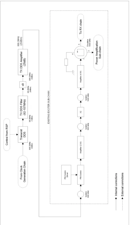
The transmitter RF block diagram is shown in gure (2.8) (adapted from [1]). The transmitter chain consists of three (3) sub-chains:
2.3.2.1.1.1 Exciter sub-chain
Refer to the Exciter sub-chain section of gure (2.8).
In this chain the RF source, a crystal oscillator with 8 selectable frequencies, is multiplied nine (9) times and fed into a directional coupler. This coupler outputs the signal via the main port to the power amplier sub-chain while the second attenuated port is connected to the LO sub-chain.
The actual transmit pulse width of either 6,6µs or 13,3µs (depending on the operational range setting) is
generated by means of the PIN switch and amplied before being routed to the two (2) times multiplier. The transmit signal, now at the actual transmit frequency of between 1,75-1,85GHz passes through a second internal amplication stage. Three (3) isolators are implemented to protect the preceding modules in the event that power should be reected. The isolators allow forward transmission of the signal, but largely attenuates it in the reverse direction.
The signal is physically connected from the output of the exciter chain to the power amplier chain by means of two circulators[1].
2.3.2.1.1.2 Local Oscillator sub-chain Refer to the LO sub-chain section of gure (2.8).
The LO sub-chain is used to generate a signal for the receive chain to be able to mix the received signal down to base band. The LO frequency is derived from the exciter chain, amplied and multiplied by two (2) to produce the same frequency as the transmitted pulse. The signal then passes through a calibration attenuator and splits into two signals (in-phase (I) and quadrature-phase (Q)) by a power divider. These two outputs are then directly fed into the receiver mixers where the received signal is mixed down to base band[1].
2.3.2.1.1.3 Power Amplier sub-chain
Refer to the Power Amplier sub-chain section of gure (2.8).
The transmit pulse generated in the exciter chain is amplied here to the transmit power level and routed to the antenna. The amplication is done in three (3) stages: Firstly, a 30W amplier stage, followed by a 100W stage and nally a 200W amplier producing a minimum transmit power of 115W at the RF output connector. The high power signal is fed to the antenna through a dual directional coupler. One port is connected to a detector diode to continuously monitor the level of the transmitter power and provide information in the event it should fail. The second port is used for test purposes[1].
The power amplier chain is connected to the antenna by means of a circulator to route the outgoing signal to the antenna.
The receiver as shown in gure (2.9) (adapted from [1]) consists of two (2) sub-chains: 2.3.2.1.2.1 Receiver Front End sub-chain
Refer to the Receiver Front End sub-chain section section of gure (2.9).
The Receiver Front End (RFE) chain is used to amplify the small returning signal whilst adding minimal noise to the signal. It is fed from the antenna via the same circulator which connects the transmit chain to the antenna module. The received signal is passed through a dual port directional coupler which is used for maintenance functionality (self test injection and VSWR fault detection). Next the signal passes through a band pass lter bank and limiter modules.
Next a PIN attenuator module is used for the implementation of the Instantaneous Automatic Gain Control (IAGC) and Sensitivity Time Control (STC) features of the receiver. The IAGC is used to prevent the receiver from saturation as result of large received signals due to clutter. The STC on the other hand varies the sensitivity of the receiver as a function of time (and thus range). Reected signals of objects close to the transmitter will be attenuated more than those of objects further away. This eectively removes excessive clutter close to the receiver. The level of the STC is also selectable as one of ve (5) positions. Lastly, the signal is amplied by a Low Noise Amplifier (LNA) and passed to the main receiver sub-chain via a circulator [1].
2.3.2.1.2.2 Main Receiver Chain
Refer to the Main Receiver sub-chain section section of gure (2.9).
The function of this chain is to mix the received signal down to base band and add sucient amplication to the signal before it is routed to the signal processor.
The received signal is rstly limited due to possible high power leakage into the receiver. A PIN attenuator is implemented to minimize leakage during the transmission period.
A lter bank band passes the signal according to the selected frequency. This is done to limit the noise in the system. The signal is now amplied again by means of a LNA unit.
The signal is then passed through a PIN switch which operates as the inverse of the PIN switch in the transmitter and so prevents the mixers from damage during the transmission period. Thus if the transmitter is on, the receiver is switched o.
The signal is then split by the power detector. One half is used to operate the IAGC while the other is split again (by the power divider) and used to feed the mixers which down converts the received signal to base band I and Q signals. Lastly the I and Q signals are amplied in the video amplier and routed to the signal processor[1].
2.3.2.2 Signal Processor Unit
The purpose of the Signal Processor Unit (SPU) is to convert the raw received radar signal into usable information for the operator by means of the radar display. The SPU consists of eleven (11) analogue and digital cards consisting of the Sync card, Pulse Repetition Frequency (PRF) Filters, Decision Correlator and Line Transceivers. All these cards plug into a motherboard back-plane which provides communication channels between the cards.
The SPU receives all the returning radar signals which includes all clutter and target information. The signal is rstly processed by means of PRF Filters to eliminate all clutter returns and returns of targets with velocities less than 180km/h. These ltered signals are then routed to the aircraft decision circuits. A further parallel lter is used to lter all Doppler returns below 400km/h so to eliminate helicopter body returns. The ltered signal now contains blade ash returns of speeds higher than 400km/h and is routed to the helicopter decision circuit.
The PRF Filters (also known as Doppler Filters) consist of four (4) cards - two for the I channel and two for the Q channel. These remove clutter and produce ten (10) range gate sampling circuits per lter card which result in the range resolution of 1km/bin for the 10km range setting or 2km/bin for the 20km range setting. Decision making is done per range cell. The energy in each cell is subjected to an energy based decision and followed by the summation of the I and Q channels. Positive target decisions are indicated by means of a positive logic signal for each target detected. Mid-range decisions are subject to the same process and all output signals are fed to the correlator unit.
The correlator combines both helicopter and aircraft decision channels and performs scan to scan correlation on this data to eliminate possible false positives.
Finally all the processed information is send to the Line Transceiver which modulates the data and routes it to the display unit[1]. The SPU block diagram is shown in gure (2.10) (adapted from [1]).
Figure 2.10: Signal Processing block diagram
2.3.2.2.1 Target Detection Target detection is done in the signal processor by means of 20 parallel and identical detection circuits called Decision Circuits. Two (2) circuits per range bin are used (and triggered accordingly): One for I-channel data and the other for Q-channel data. These 20 detection circuits are duplicated to result in detection circuits for both xed wing aircraft and helicopters resulting in 40 circuits.
Figure 2.11: Block diagram of a single aircraft detection circuit
The absolute value from both the I-channel and Q-channel are combined to produce an approximation of the magnitude, i.e. |I|+|Q| ∼ p
I2+Q2. Integration of this magnitude is done in the target integrator. This
integrator is cleared at the end of each sector break of 10◦.
Noise is also continuously integrated using the noise integrator which is supplied by means of the Q-channel data. This gives a measurement of the noise present in the system. This integrator is also not reset as is the case in the target integrator.
When a target is encountered, both the target and noise integrators rise due to the returning signal. The value of the target integrator rises quicker than the value of the noise integrator due to a shorter rise time. The output of the target and noise integrators are compared and if the target integrator value is higher than the value of the noise integrator, a target is declared in the particular range bin. The detection is routed via the signal processor to the Operator module where the corresponding light will be lit in azimuth and range to indicate a target.
This process is identical in all ten (10) range bin detection circuits for both the aircraft and helicopter channels. This design is very complex since a large number of detection circuits are used. It could easily happen that some of these circuits are faulty or biased incorrectly without the user knowing this.
2.3.2.3 RF performance measurements
Various RF measurements were planned for the ERS. These included the measurement of the Minimum de-tectable signal (MDS) of the receiver which is specied to be -115dBm. RRS attempted this measurement, but it was not possible with the available test equipment. The value of -115dBm however seems rather high and a mathematical approximation of the MDS was calculated to be -128dBm (refer to Appendix (E.2.1).
2.3.3 Operator Module
The PPI consists of a display with concentric circles of Light Emitting Diodes (LED) to indicate the target bearing and range. The PPI was previously replaced by RRS with an integrated PPI and remote control unit which is personal computer based.
This upgraded PPI runs on a laptop computer and has the same functionality as both the original PPI and remote control units. As an additional feature, a Global Positioning System (GPS) unit was added by RRS to x the radar system's location. Using the remote operation setting, the transceiver module can be fully controlled and congured from the operator module.
Figure (2.12) shows the Operator module.
2.4 Conclusion
In this chapter the existing ERS was discussed on modular level to provide a base for the modied version discussed in Chapter 3. Emphasis was placed on the transceiver module and more in particular the transmit and receiver chains as well as the signal processor since all the modications needed to implement pulse compression were done in this module.
Chapter 3
Modied Eekhoring Radar System
3.1 Introduction
This project aims to use the existing ERS as a development bench and implement advanced digital signal processing techniques with the main improvement being the improvement of the limited range resolution of the system. In the existing system, the range resolution is dened by ten (10) xed range bin detection circuits of the signal processor. This results in a xed range resolution per operational range setting.
The existing signal processor is replaced with a new rmware based signal processor running on a single FPGA device. The main upgrade feature of the new signal processor is the implementation of Digital Pulse Compression and Doppler Processing techniques to improve the range resolution.
Implementing pulse compression however required a relative large number of modications to the RF subsystem of the ERS. The amount of RF modication work required was largely underestimated and resulted in the project taking much longer than what was anticipated.
This chapter rstly describes the RF subsystem modications and the RF modules required to implement these modications. Secondly an overview of the newly designed RSP for the implementation of the techniques above is given. This RSP is designed, but only partially tested due to time constraints. The pulse compression section implemented will be discussed with results.
3.2 Transceiver Modications
Only the transceiver was modied in this project leaving the antenna and operator modules unchanged. (The operator module was to be an existing PC based moving target indicator (MTI) processor to indicate detections and show target movement and information. This was not implemented.)
At rst the changes to the RF subsystem of the transceiver was envisaged to be minimal. However as the project progressed it was found that a large number of modications had to be made to the transmit and receive chains to be able to implement pulse compression techniques and thus improve the range resolution of the ERS. The existing signal processor was replaced entirely with a FPGA based digital signal processing board. Some existing timing signals were utilized to keep the changes to the RF subsystem to a minimum. Frequency planning was done to ensure that the system is synchronous.
Figure (3.1) shows a block diagram of the interconnections of the upgraded ERS.
The modications were implemented in an metallic case allowing for the easy connection of the relevant modules. Figure (3.2) shows a photograph this case.
Figure 3.2: Photograph of the transceiver modication case
3.2.1 RF Subsystem
The modications made to the RF subsystem are: 3.2.1.1 Transmitter chain
Modications to the transmitter module were done in the clock generation, exciter and LO chains. Refer to gure (3.1) which shows a simplied block diagram of the modied transmit chain.
The existing exciter chain was modied to produce two (2) chains: The one the clock generation sub-chain and the other the pulse modulation sub-chain.
The existing 9-time frequency multiplier modules were replaced due to these modules having a high failure rate. This replacement also required an amplier module at the end of the exciter chain to produce an equivalent
chain output power level to the unmodied chain. Two (2) lters were also introduced to suppress harmonic and spurious signals.
The main modication however was the introduction of a Direct Digital Synthesizer (DDS) module in the existing exciter chain. This DDS module was used to phase modulate the transmission pulse with a pulse compression code to improve range resolution in the RSP.
The modications to the various chains in the transmitter module with results of the newly introduced compo-nents are given in the following sections.
3.2.1.1.1 Clock Generation sub-chain
The Clock Generation chain is used to distribute various clock signals, generated from a single frequency source, to the RSP board, LO and Transmit sub-chains.
The output of the existing variable frequency source was xed to 98.8MHz and band pass ltered. The resulting signal was split to provide signal paths for the RSP Clock and the rest of the Transmit chain. The one splitter output to the RSP Clock is amplied to 15-16 dBm required by the RSP board while the other is output is frequency multiplied nine (9) times. This is implemented by means of a new 9-times frequency multiplier module replacing the existing one.
The output of the 9-times frequency multiplier module is split again and routed to both the LO and pulse modulation chains.
Figure (3.3) shows the block diagram of the Clock Generation chain with applicable signal levels.
Figure 3.3: Functional block diagram of the Clock Generation sub-chain
3.2.1.1.1.1 Clock Filter
Refer to Appendix B.3 for a full functional description of this module.
This module is used to band pass lter the output of the system oscillator. Figure (3.4) shows the rst, second and third order harmonic signal suppression. The centre frequency is 98MHz and the lter bandwidth is±14,5MHz. The signal loss at the centre frequency is 1,8dB.
Figure 3.4: Harmonic signal power levels of the system oscillator lter module
3.2.1.1.1.2 RSP Clock Amplier
Refer to Appendix B.5 for a full functional description of this module.
With an input frequency of 98,8MHz at a signal power level of 5,7dBm, the output power level was measured to be 15,7dBm (the minimum required level is 13dBm). This results in the amplier providing a gain of 10dB. Figure (3.5) shows the output of the amplier module. Spurious signals are at a level of 65,3dBc away from the fundamental.
Figure 3.5: Measured output signal of the RSP clock amplier module
3.2.1.1.1.3 9-Time Frequency Multiplier
Refer to Appendix B.1 for a full functional description of this module.
This module is used to multiply the system clock of 98,8MHz to 889,2MHz, the reference frequency used by the two (2) DDS modules. Given an input frequency of 98,8MHz at a power level of 0dBm the output was found to be 889,2MHz with a power level of 6,7dBm. Figure1(3.6) shows the bandwidth of the multiplier at the -3dB
points to be 11,5MHz.
1Note that these graphs were taken directly from the spectrum analyzer instrument. Frequency is on the x-axis with far-left the start and far-right the stop frequencies. The centre frequency is in the middle of the image. The logarithmic y-axis shows the signal power level indBm. Sometimes a peak table is available showing the marker values.
Figure 3.6: Bandwidth of the system clock frequency multiplier module
3.2.1.1.2 Pulse Generation sub-chain
Derived from the existing exciter chain, the pulse generation sub-chain is used to generate the coded transmis-sion pulse which is compressed in the RSP on reception. A modulation frequency of 2,53125MHz2is implemented
and this bandwidth was designed for throughout the RF subsystem. The transmission pulse is phase modulated by means of a Direct Digital Synthesizer (DDS) module.
The Transmit DDS module, using the 900MHz output from the clock generation sub-chain, outputs a modulated transmit pulse at 1
9th the input frequency. Thus eectively returning to the frequency output by the frequency
source in the clock generation sub-chain. The pulse modulation code is controlled by the RSP and is discussed later in this chapter (refer to section (3.2.2.4)).
This results in the need for a times-9 frequency multiplier unit to produce the 900MHz signal needed in the power amplication sub-chain. The output of the Transmit DDS module is bandpass ltered to suppress harmonic and spurious signals before the times-9 multiplication. The signal level needs to be amplied to 25dBm before being routed back into the rest of the transmit chain.
The existing times-9 multiplier modules included an amplier with a 25dB gain. This amplication in the modied system was achieved by using the existing problematic modules, but with the times-9 multiplier section disabled thus directly routing the new times-9 module to the amplier section of the old module. The output frequency is 889,2MHz at a signal power level of 25dBm. The rest of the existing exciter chain is used in which the transmit pulse is multiplied and amplied before being routed to the power amplication chain by means of two (2) circulators as per Chapter 2.
The output of the pulse generation chain is a modulated transmit pulse of 13,3µs repeated every 160µs (the
PRI) which is generated by means of the PIN switch.
Figure (3.7) shows the block diagram of the pulse generation sub-chain with relevant frequencies and signal power levels.
Figure 3.7: Functional block diagram of the pulse generation sub-chain
3.2.1.1.2.1 Pulse Generation DDS Module
Refer to Appendix B.2 for a full functional description of this module.
The DDS module receives a reference clock signal of 889,2MHz and generates the modulated output frequency of 98,8MHz. The actual pulse modulation code is controlled by the RSP and implemented by selecting two (2) preset frequency and phase oset proles of the DDS module. The setup values for the DDS module is calculated below.
Using equation (B.1) the Frequency Tuning Word (FTW) can be calculated as: 98,8×106 = (F T W)(889,2×10 6) 232 F T W = (98,8×10 6)(232) 889,2×106 = 477218588.44444400
The Frequency Tuning Word (FTW) is an integer value and rounded to F T W = 477218588. Using the
rounded FTW the actual output frequency is 98799999,91MHz. Two proles (3 and 4) were loaded with the FTW as above. The Phase Offset Word (POW) for prole 3 was loaded asP OW = 0while the POW for
prole 4 was calculated for a90◦ phase oset to be:
P OWprof ile4 =
90 360 ×2
14
= 4096
Care must be taken during frequency planning since the DDS module generates a −63dBc spurious signal at
REF CLK
8 :
For the transmit DDS module this spurious signal is located at:
fspur =
889,2 8
= 111,15 [M Hz]
This is out of the operational range of the transmitter chain.
Figure (3.8) shows the output frequency and signal power level of the transmit DDS module when prole 3 was selected.
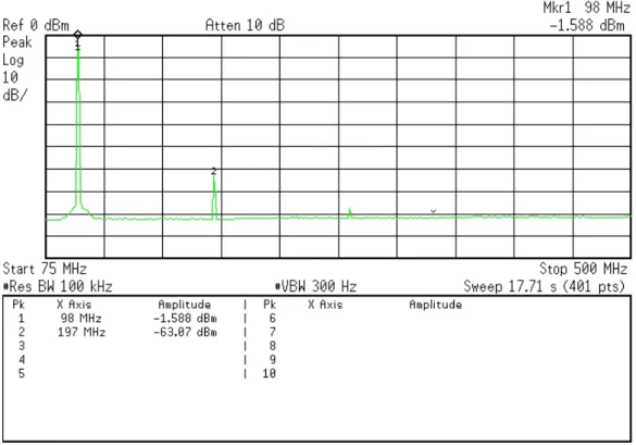
Figure 3.8: Output frequency and signal power level of the transmit DDS module
3.2.1.1.2.2 DDS Output Filter
Refer to Appendix B.3 for a full functional description of this module.
The DDS lter is used to lter the harmonics signals at the output of the DDS module. Figure (3.9) shows the bandwidth of the DDS lter module while gure (3.10) shows the harmonic suppression of the lter. The centre frequency is 99,1MHz and the lter bandwidth is±15,5MHz. The signal loss at the centre frequency is 1,59dB.
Figure 3.10: Harmonic signal power levels of the transmit DDS lter module
3.2.1.1.2.3 Times-9 Frequency Multiplier
Refer to Appendix B.1 for a full functional description of this module.
The times-9 multiplier module is used to multiply the output of the DDS lter back to 889,2MHz allowing the output to be routed to the rest of the existing exciter chain. Given an input frequency of 98,8MHz at a power level of 0dBm the output was found to be 889,2MHz with a output power level of 5,7dBm. Figure (3.11) shows the bandwidth of the multiplier at the -3dB points to be±37MHz.
3.2.1.1.2.4 DDS Amplier
Refer to Appendix B.4 for a full functional description of this module.
The DDS amplier is used to amplify the output of the frequency multiplier module to the required power level of±25dBm. With a centre frequency of 889,2MHz and a signal power level of 0dBm the gain was found to be
23,49dB. Figure (3.12) shows the bandwidth of the amplier at the -3dB points to be±82MHz.
Figure 3.12: Bandwidth of the transmit DDS amplier module
3.2.1.1.3 Local Oscillator (LO) sub-chain
In the existing ERS transmit chain, the same frequency used for the transmit pulse is used in the receive chain to mix down the returning signal to base band. The Analogue to Digital (ADC) converter used in the upgraded RSP performs IF sampling.
It was thus needed to modify the existing LO chain to generate an IF signal at the output of the receive chain mixer. This requires the LO chain to produce a frequency which is oset to the transmission frequency. The same DDS design setup as in the pulse generation sub-chain is used, but the DDS module outputs an oset frequency to the actual pulse generation sub-chain as per section (3.2.1.1.2).
The LO sub-chain receives a reference clock of 889,2MHz from the clock generation sub-chain as input to the DDS module. The oset frequency output of the DDS module is band pass ltered and routed to a times-9 module. This times-9 module is the same design as the other times-9 modules, but the internal lters have been tuned with respect to the oset frequency. Finally the signal is amplied to the correct power level before being routed back into the existing LO sub-chain where it is multiplied and amplied again to be routed to the receiver mixer.
The oset frequency is calculated to be an 1
18th of the IF frequency of 70,875MHz. The 1
18th factor is due to
fLO DDS = fP M DDS+ fIF 18 = 98,9 + 70,875 18 = 102.7375M Hz
Figure (3.13) shows the block diagram of the modied LO sub-chain. The applicable frequencies and power levels are indicated for the modied section.
Figure 3.13: Functional block diagram of the LO sub-chain
3.2.1.1.3.1 LO DDS Module
Using equation (B.1) the FTW can be calculated as:
fLO DDS = (F T W)(889,2×10⁶) 232 F T W = (102,7375×10 6)(232) 889,2×106 = 496237294,9
When rounded, theF T W = 496237295and this was implemented. Using the rounded FTW the actual output
frequency is 102,7375MHz. Only one prole was needed and the POW was set to zero.
The spurious signal for the LO DDS module is located at the same frequency as for the transmit DDS module.
fspur =
889,2 8
= 111,15 [M Hz]
Figure (3.14) shows the output frequency and signal power level of the LO DDS module.
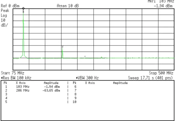
Figure 3.14: Output signal power level of the LO DDS module
3.2.1.1.3.2 DDS Output Filter
Refer to Appendix B.3 for a full functional description of this module.
This module has the same functionality as the previous lter, but is used at the output of the LO DDS module. Figure (3.15) shows the harmonic suppression of the LO DDS lter module. The centre frequency is 102,3MHz and the lter bandwidth is±15,8MHz. The signal loss at the centre frequency is 1,9dB.
Figure 3.15: Harmonic signal power levels of the LO DDS lter module
3.2.1.1.3.3 9-Time Frequency Multiplier
Refer to Appendix B.1 for a full functional description of this module.
This module is used to multiply the output of LO DDS lter up from 102,74MHz to 924,64MHz. The output is then routed back into the existing LO sub-chain. Figure (3.16) shows the bandwidth at the -3dB points of the LO DDS frequency multiplier module to be ±27MHz. An input signal power level of 0dBm produced a 3dBm
signal at the output.
3.2.1.1.3.4 DDS Amplier
Refer to Appendix B.4 for a full functional description of this module.
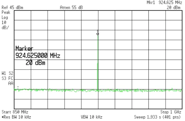
The LO DDS amplier is used to amplify the output of the LO DDS frequency multiplier module to the required power level of±25dBm. With a centre frequency of 924,64MHz and a signal power level of 0dBm the gain was
found to be ±20dB. Figure (3.17) shows the output power level of the module (the bandwidth is not needed
since the LO frequency does not change).
Figure 3.17: Output signal power level of the LO DDS amplier module
(Note that the full range of the testing instrument was not used when this measurement was generated.) 3.2.1.2 Receive Chain
This receive chain was only modied at the end of the main receiver sub-chain to accommodate the IF sampling requirement of the ADC module in the RSP.
Refer to the receive chain section of gure (3.1) for a block diagram of the receive chain. 3.2.1.2.1 Main Receiver sub-chain
The I-channel feed to the Video (or Base Band) amplier module in the existing system was routed via an IF amplier module to amplify the mixed down received signal for sampling by means of the ADC in the RSP. A band pass lter module was introduced at the output of the IF amplier to band pass lter the signal mainly to minimize noise and to lter harmonics signals.
3.2.1.2.1.1 IF Amplier
The IF amplier is used to amplify the output of the receiver mixer to produce the 10dBm signal power level for the ADC to operate optimally. The measured gain at the IF frequency of 70.875MHz was 40dB.
3.2.1.2.1.2 IF Filter
To minimize the noise at the input of the ADC in RSP, the output of the IF amplier module passes through an IF lter module. Figure (3.18) shows the bandwidth of the IF lter module. The centre frequency is 71,2MHz and the lter bandwidth is±10MHz. The signal loss at the centre frequency is 0,9dB.
Figure 3.18: Bandwidth of the IF lter module
3.2.1.3 RF Performance measurements
Various RF measurements were planned for the modied transceiver. These included the MDS and an end-to-end measurement of the system. These measurements however were never done due to the system not being in a testable state.
3.2.2 Signal Processor Modications
3.2.2.1 Overview
The existing ERS has a range resolution of 2km which is determined by the ten (10) PRF lter circuits in the signal processor. The primary aim of this project was to improve on this limiting factor. To improve the range resolution of the existing radar system, two (2) signal processing techniques were implemented: Digital Pulse Compression and an increased number of range bin target detection circuits.
The implementation of a pulse compression, as explained later in chapter (3.2.2.4), produces a compressed version of the transmit pulse. This improves the range resolution, while keeping the higher detection capabilities of a long pulse system.
Range resolution is improved by dening more range bins target detection circuits in the RSP than the existing ten (10) bins. Doppler processing is implemented on these increased number of range bins and the Doppler-shift generated by a moving target is computed which allows for the elimination of clutter.
The entire signal processor was replaced by a digital signal processor running on a dedicated development board. All signal processing is done on a single FPGA device. Refer to Appendix B.7 for a detailed description of the Altera Digital Signal Processing Evaluation Board used to implement the new RSP.
The RSP was fully designed but not fully implemented and tested due to time constraints. The sections implemented and tested will be discussed later. After implementation of almost the complete RSP (which included a 32-bit micro controller), it was found that only 25% of the available capacity was utilized. The amount of on-chip memory was the limiting factor, but this can be solved using external memory and creative techniques.
This section gives an overview design of the RSP and discusses the design and implementation of the RSP with regards to timing generation to ensure the radar system is synchronous, Pulse Compression design and imple-mentation as well as impleimple-mentation and results achieved by the down conversion chain and pulse compressor modules.
3.2.2.2 Quadrature Sampling of the IF signal
Since both the in-phase (I) and quadrature (Q) received signals are required for processing in this RSP, while using a single ADC, quadrature was implemented.
Quadrature sampling refers to the oversampling of a carrier signal (here the IF frequency) at four (4) times the frequency of the carrier and is shown in the following equation:
fsample = 4 fIF
This results in the signal being sampled every 90◦. By combining the 0◦and 180◦samples into a data stream and the 90◦and 270◦into a second, two outputs are generated containing the I-channel data and the Q-channel data respectively. It is noted that the 180◦and the 270◦sampled results are negative and this should be compensated for.
The output of the I-channel data is of the form I, -I, I, -I, etc. while the Q-channel produces data of the form Q, -Q, Q, -Q, etc. Should the signal not be split, the output of the ADC results in giving I, Q, -I, -Q,I, Q, -I, -Q sample outputs.
The bandwidth of the pulse modulation implemented in this project is 2,53125MHz resulting in a Nyquist frequency of 5,0625MHz for a single channel and thus a minimum frequency of 10,125MHz is required to be able to represent both the I-channel and Q-channel data once sampled.
The representation of the complete IF signal is not of interest and thus down sampling can be used where the sampling frequency does not comply to the Nyquist theorem. The equation[2] of
fsample = =
4fIF
2n+ 1 (3.1)
(wheren= 1,2,3,4, ...) can be used to select the an IF and sampling frequency pair. A maximum value for n
is thus selected to minimize the sampling frequency while still complying to the Nyquist requirement for the bandwidth of the signal.
Originally a base RSP clock frequency of 81MHz was selected to allow for the use in the RSP was well as to replace the system clock of 9MHz in the existing ERS which generates the transmit trigger pulse. This resulted
in the selection of the sampling frequency of 40,5MHz. Using equation (3.1) and n= 3, the corresponding IF
frequency was calculated to be:
fIF =
7fsample
4 = 70,875M Hz
This is an easy frequency to implement in the transmit and receive chains by means of LO sub-chain frequency oset setup and IF amplication and ltering.
3.2.2.3 Frequency Planning and Synchronization
It is fundamental that the radar system must be synchronous and coherent. To achieved this a single frequency source must be used to generate all frequencies and timing signals and these signals must be synchronized to a particular event.
In the upgraded system the frequency source of 98,8MHz was used throughout the system to derive and generate all frequencies and timing signals. The synchronization of the system is achieved by triggering events on the Transmit Trigger Pulse supplied by the existing transceiver. This pulse indicates when the transceiver is generating the transmit pulse.
Figure (3.20) shows a block diagram for the timing distribution of the upgraded transceiver. Fundamentally the system is synchronized on the Radar Synchronization Clock of 10.125MHz which is derived from the frequency source by means of a Phase Lock Loop (PLL).
In this setup the output of the LO and Transmit chains, generated by the two (2) DDS modules are regarded as two (2) free running clocks and are both driven by the frequency source. At the output of the Receiver chain, the frequency of the IF signal produced is 70,875MHz (the reason will become clear next).
In the RSP, the frequency source is used to drive the PLL which produces an output frequency of 81MHz. This output is divided by two (2) to derive the Sample Clock frequency of 40.5MHz. The Sample Clock is in turn divided by four (4) to give the RSP Synchronization Clock of 10.125MHz.
Having a closer look at the IF and Sampling frequencies, it is found that these two are factors of the RSP Synchronization Clock of 10.125MHz:
fIF = 7×fRSP SY N C CLK
and
fSAM P LE = 4×fRSP SY N C CLK
Referring to the IF Sampling section of this chapter (section (3.2.2.2)), it is required that the IF and sampling frequencies have a relationship of 7
4. Thus, if this system is synchronized to the RSP Synchronization Clock of
10,125MHz, the system is regarded to be synchronous.
The system synchronization is done by means of the Transmit Trigger Synchronizer module. This module is used to sample the external transmit trigger event, and synchronize this to the RSP Synchronization Clock. The output of this module is used to reset the clock divider that generates the Modulation Clock of 2,53125MHz used to control the Pulse Generation DDS module which in turn generates the modulated transmission pulse in the Transmit chain.
3.2.2.4 Pulse Compression Implementation 3.2.2.4.1 Pulse Compression Overview
The ERS has a limited range resolution of 2km This equates to ten (10) range bins for the 20km operating range setting. When the operating range of 10km is selected, the range resolution improves to 1km This limited resolution is due to the xed number of hardware range lters in the system. Each lter represents a range bin in which a target may be present.
One solution to increase the range resolution is to shorten the transmit pulse width, but this requires an increase in the peak power of the transmitter to maintain the radar's operational range. Increasing the peak transmit power on the other hand requires upgrades to the transmitter power amplier sections which will increase the radar in size, design diculty, and most importantly, in price.
Another technique is to modulate the transmit pulse into sub-pulses and spread it over time, which in turn will increase the average transmitter power and lower the peak power. This however increases the processing complexity. The technique is called Digital Pulse Compression[13, 8, 17] (or just pulse compression).
Pulse compression entails the transmission of a long modulated pulse and the processing of the returned signal to produce a relatively narrow pulse. Pulse compression is implemented in both the transceiver and the RSP
of a radar system, where the transceiver modulates (under the control of the RSP) the outgoing pulse and the RSP processes the returned echo.
The requirements for pulse compression in this project, the selection of a suitable pulse code and results achieved are discussed next.
3.2.2.4.2 Project Pulse Compression design
Pulse compression was done by convolution of the encoded received pulse with a copy of the encoded transmit pulse. When these two match up precisely, a large peak is produced. The range to the target is then determined by means of where this peak is located in a particular PRI. Since convolution in the time-domain equates to multiplication in the frequency-domain, Fast Fourier Transform (FFT) methods were used to compress the pulse.
RRS provided a VHDL based Pulse Compressor module to be used for this project. 3.2.2.4.2.1 Modulation of the transmit pulse
The transmit pulse was 180◦ phase modulated by using the transmit DDS module to generate the phase
oset by means of selecting the correct preset proles at the modulation frequency of 2,53125MHz. Due to the two-times multiplier in the transmit chain of the transceiver the actual phase oset implemented by the DDS module was90◦ which, when multiplied by two (2), will produce the required phase oset of180◦in the signal
transmitted by the antenna.
Figure (3.21) shows the phase oset generated at the output of the DDS module as a90◦ phase oset is added.
This is implemented by selecting the correct prole of the DDS (refer to the detailed description of the DDS module in Appendix B.2).
Figure 3.21: The output signal of the transmit DDS performing a90◦phase shift.
The transmit pulse was divided into sub-pulses. The number of sub-pulses where calculated as follows:
N = τtx τmod
= (13,3×10 )(2,53125×10 ) = 33,666
' 32
whereN is the number of sub-pulses,τtx the transmit pulse width andτmod= fmod1 the modulation period and
frequency.
Since only integer values can be implemented, the number of sub-pulses were rounded to N = 32 for easy
implementation in digital systems.
By switching between these two DDS proles, a phase-code is modulated on the transmit signal. The particular code pattern and design is discussed in the next section.
3.2.2.4.2.2 Phase-coded waveform design
Other than with FM waveform modulation, phase-coded waveforms sub-divide the transmit pulse into a number of sub-pulses[14, 9]. These sub-pulses carry a particular phase and is of equal length. Many types of phase-coding exist of which the most popular are bi-phase (or binary) and poly-phase coding.
Binary phase-coding implements a sequence of 0s and 1s resembling a0◦or180◦ phase shift respectively in
the transmit pulse as shown in gure (3.22) as an example.
Figure 3.22: An example of a binary phase-coded signal.
Side-lobes are generated when the returning pulse is compressed, but with proper waveform design these side-lobes can be kept to a minimum. Side-side-lobes generated images of detected targets and produce false information. Side-lobe suppression must be implemented to prevent false detection but is not implemented here.
A special class of binary codes, called Barker codes, has the property that the peak of the auto-correlation function is equal to the number of sub-pulses while the maximum peak side-lobe is 1. Only thirteen (13) of
An existing phase-code optimizing Matlab program was adapted3 and used to produce the 32-sub-pulse code
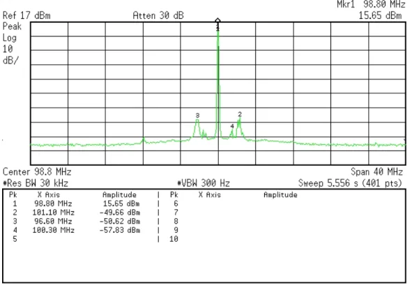
needed. The software generates random 32-bit phase-codes, compresses each and compares it to a previous result in having the smallest side-lobes. Compression is done by taking the FFT of the random phase-code, multiplying it with itself (thus doing a time-domain convolution) and taking the IFFT to convert back to the time-domain. After numerous runs the best waveform found during simulation can be used. Figure (3.23) shows a compressed pulse and the generated side-lobes which are located at around -16dB. Note that the result is symmetrical around the origin.
Figure 3.23: Time-domain response of an optimized phase-coded compressed pulse
The waveform selected for this project by means of simulation was: 1 0 1 0 0 0 0 1 0 0 1 0 0 1 1 0 0 1 1 1 1 0 1 0 0 0 1 1 1 1 0 0. The software code can be adapted to generate a number of these low side-lobe codes. The radar system will then be able to implement these codes randomly from pulse to pulse.
To compare this result, an optimal binary code with 32-sub-pulses was used as per the Radar Handbook by Merril I. Skolnik (page 10.18) in the same Matlab program. Figure (3.24) shown the compressed pulse of this particular code. Side-lobes are located below -20dB which would make this a better selection. The computed code was used for further computations.
Figure 3.24: Time-domain response of a 32-bit optimal binary code obtained in the Radar Handbook (Merril I. Skolnik, page 10.18)
3.2.2.4.2.3 Implementation The RSP contains both the controls for the transmission of the phase-code via the DDS module as well as the Pulse Compressor module4. On the up-going ank of the transmit trigger
pulse, the RSP starts to implement the selected modulation sequence. Figure (3.25) shows the phase-coded output control signal. The top trace is the sync-pulse, middle the control signal and bottom the output signal of the transmit DDS module. The last is however of too high a frequency to see the phase shift.
Figure 3.25: Figure of the phase-coded control signal waveform code
The actual compression of the pulse by means of the RSP was conrmed by means of a software vs. hardware simulation result. The results are given in section (3.2.2.6) of this chapter where the pulse compressor section was tested.
3.2.2.4.2.4 Bandwidth problems
To test the modulation of the transmit chain, the transmit signal was routed back into the receiver chain. The signal was routed out of the transmitter chain just after the two-times multiplier module and before the 4W amplier. It was routed back into the receiver chain, with sucient attenuation to protect the receiver modules, at the mixers.
The mixed signal, now at the IF frequency, showed dead zones after each phase change. After further investi-gation, the problem was traced back to the transmit chain 9-times frequency multiplier module. By means of a simulation it was found that on doing a phase-change, higher frequency components of up to 110MHz were generated while the input bandwidth of the module was only later calculated to be only (37
9 = 4,1MHz).
When this signal passes through the transmit 9-times frequency multiplier, the internal lters attenuate the signal due to the limited input bandwidth. This lower signal power causes the tripler sections of the 9-times frequency multipliers to switch o and thus no output signal is generated. These triplers require a minimum input power level of -2dBm to operate. Figure (3.26) shows the dead zones as measured by means of a diode-detector on the bottom trace. Figure (3.27) is a zoomed picture.