August 2005
F
AN5333A/F
AN5333B High Efficienc
y
, High Current Serial LED Driver with 30V Integrated Switc
h
FAN5333A/FAN5333B
High Efficiency, High Current Serial LED Driver with 30V
Integrated Switch
Features
■ 1.5MHz Switching Frequency ■ Low Noise
■ Adjustable Output Voltage ■ Up to 1.5A Peak Switch Current ■ 1.5W Output Power Capability ■ Low Shutdown Current: <1µA ■ Cycle-by-Cycle Current Limit ■ Low Feedback Voltage ■ Over-Voltage Protection
■ Fixed-Frequency PWM Operation ■ Internal Compensation
■ FAN5333A has 110mV Feedback Voltage ■ FAN5333B has 315mV Feedback Voltage ■ Thermal Shutdown
■ 5-Lead SOT23 Package
Applications
■ Cell Phones ■ PDAs ■ Handheld Equipment ■ Display Bias ■ LED Bias ■ Flash LEDDescription
The FAN5333A/FAN5333B is a general purpose LED driver that features fixed frequency mode operation and an integrated FET switch. The device’s high output power makes it suitable to drive flash LEDs in serial connections. This device is designed to operate at high switching frequencies in order to minimize switching noise measured at the battery terminal of hand-held communications equipment. Quiescent current in both normal and shutdown mode is designed to be minimal in order to extend battery life. Normal or shutdown mode can be selected by a logic level shutdown circuitry.
The low ON-resistance of the internal N-channel switch ensures high efficiency and low power dissipation. A cycle-by-cycle cur-rent limit circuit keeps the peak curcur-rent of the switch below a typical value of 1.5A. The FAN5333A/FAN5333B is available in a 5-lead SOT23 package.
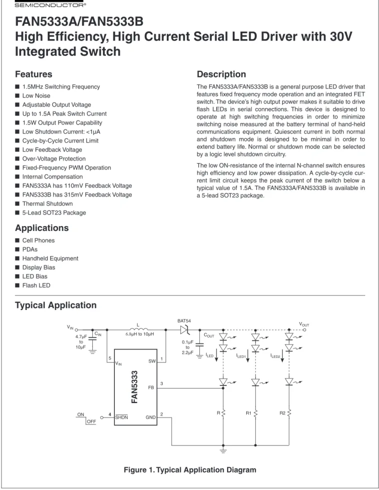
Typical Application
Figure 1. Typical Application Diagram
SHDN VIN VOUT R GND VIN FB SW CIN 6.8µH to 10µH 1 3 2 4 5 4.7µF to 10µF COUT L BAT54 ILED 0.1µF to 2.2µF ON OFF ILED2 ILED1 R1 R2FA
N5333
F
AN5333A/F
AN5333B High Efficienc
y
, High Current Serial LED Driver with 30V Integrated Switc
h
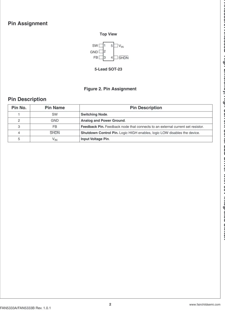
Pin Assignment
Figure 2. Pin Assignment
Pin Description
Pin No.
Pin Name
Pin Description
1 SW Switching Node.
2 GND Analog and Power Ground.
3 FB Feedback Pin. Feedback node that connects to an external current set resistor. 4 SHDN Shutdown Control Pin. Logic HIGH enables, logic LOW disables the device. 5 VIN Input Voltage Pin.
Top View 5-Lead SOT-23 SW GND FB VIN SHDN
F
AN5333A/F
AN5333B High Efficienc
y
, High Current Serial LED Driver with 30V Integrated Switc
h
Absolute Maximum Ratings
(
Note1)
Recommended Operating Conditions
Notes:
1. Stresses above those listed under “Absolute Maximum Ratings” may cause permanent damage to the device. This is a stress rating only and functional operation of the device at these or any other conditions above those indicated in the operational section of this specification is not implied. Exposure to absolute maximum rating conditions for extended periods may affect device reliability. Absolute maximum ratings apply individually only, not in combination.
2. Using EIA/JESD22A114B (Human Body Model) and EIA/JESD22C101-A (Charge Device Model).
3. This load capacitance value is required for the loop stability. Tolerance, temperature variation, and voltage dependency of the capacitance must be considered. Typically a 1µF ceramic capacitor is required to achieve specified value at VOUT = 30V.
Parameter
Min
Max
Unit
VIN to GND 6.0 V
FB, SHDN to GND -0.3 VIN + 0.3 V
SW to GND -0.3 35 V
Lead Soldering Temperature (10 seconds) 300 °C
Junction Temperature 150 °C
Storage Temperature -55 150 °C
Thermal Resistance (ΘJA) 210 °C/W
Electrostatic Discharge Protection (ESD) Level (Note 2) HBM 2 kV
CDM 1
Parameter
Min
Typ
Max
Unit
Input Voltage 1.8 5.5 V
Output Voltage VIN 30 V
Operating Ambient Temperature -40 25 85 °C
Output Capacitance Rated at the Required Output (Note 3) for maximum load current
F
AN5333A/F
AN5333B High Efficienc
y
, High Current Serial LED Driver with 30V Integrated Switc
h
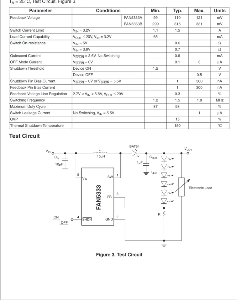
Electrical Characteristics
Test Circuit
Figure 3. Test Circuit
Unless otherwise noted, V
IN= 3.6V, V
OUT= 20V, I
LED= 20mA, T
A= -40°C to 85°C, Typical values are at
T
A= 25°C, Test Circuit, Figure 3.
Parameter
Conditions
Min.
Typ.
Max.
Units
Feedback Voltage FAN5333A 99 110 121 mV
FAN5333B 299 315 331 mV
Switch Current Limit VIN = 3.2V 1.1 1.5 A
Load Current Capability VOUT≤ 20V, VIN = 3.2V 65 mA
Switch On-resistance VIN = 5V 0.6 Ω
VIN = 3.6V 0.7 Ω
Quiescent Current VSHDN = 3.6V, No Switching 0.6 mA
OFF Mode Current VSHDN = 0V 0.1 3 µA
Shutdown Threshold Device ON 1.5 V
Device OFF 0.5 V
Shutdown Pin Bias Current VSHDN = 0V or VSHDN = 5.5V 1 300 nA
Feedback Pin Bias Current 1 300 nA
Feedback Voltage Line Regulation 2.7V < VIN < 5.5V, VOUT≤ 20V 0.3 %
Switching Frequency 1.2 1.5 1.8 MHz
Maximum Duty Cycle 87 93 %
Switch Leakage Current No Switching, VIN = 5.5V 1 µA
OVP 15 %
Thermal Shutdown Temperature 150 °C
SHDN VIN VOUT
GND R
VIN
FB
SW CIN 10µH 1 3 2 4 5 10µF COUT L BAT54 ILED 1µF ON OFF Electronic Load
FA
N5333
F
AN5333A/F
AN5333B High Efficienc
y
, High Current Serial LED Driver with 30V Integrated Switc
h
Typical Performance Characteristics
T
A= 25°C, C
IN= 4.7µF, C
OUT= 0.47µF, L = 10µH, unless otherwise noted.
2.0 2.5 3.0 3.5 4.0 4.5 5.0 5.5 50 60 70 80 90 100 50 60 70 80 90 100
Efficiency vs. Input Voltage
Input Voltage(V) Ef fi ci en cy ( % ) ILED = 10mA VOUT = 9V ILED = 20mA ILED = 30mA ILED = 40mA 2.0 2.5 3.0 3.5 4.0 4.5 5.0 5.5
Efficiency vs. Input Voltage
Input Voltage(V) Ef fi ci en cy ( % ) VOUT = 15V ILED = 20mA ILED = 30mA ILED = 40mA ILED = 10mA 2 3 4 5 0 50 100 150 200 250 300
Maximum Load Current vs. Input Voltage
Max im u m L o a d C u rren t ( m A) Input Voltage (V) TA = -40°C TA = 25°C TA = 85°C 2.0 2.5 3.0 3.5 4.0 0 50 100 150 200
Maximum Load Current vs.Input Voltage
Input Voltage (V) Max im u m L o a d Cu rren t (mA ) VOUT = 14.2V VOUT = 9.3V VOUT = 12.3V -40 -20 0 20 40 60 8 0 9 .6 9 .8 10 .0 10 .2 10 .4 10 .6 10 .8
LED Current vs Temperature
LE D Cu rren t ( mA ) Temperature (°C) VIN = 2.2V VIN = 3.6V VIN = 5.5V VOUT = 15V ILED<5% CIN = 10µF VOUT = 15V ILED<5% CIN = 10µF COUT = 1µF ∆ILED<5% CIN = 10µF COUT = 1µF -40 -20 0 20 40 60 80 1.2 1.4 1.6 1.8 2.0 SW Frequency vs Temperature Temperature (°C) SW F req u e n c y ( M Hz ) VIN = 2.2V VOUT = 15V VIN = 3.6V VIN = 5.5V COUT= 1µF
F
AN5333A/F
AN5333B High Efficienc
y
, High Current Serial LED Driver with 30V Integrated Switc
h
Typical Performance Characteristics
(Contd.)T
A= 25°C, C
IN= 4.7µF, C
OUT= 0.47µF, L = 10µH, unless otherwise noted.
2 3 4 5 0 5 10 15 20 25 VOUT = 15V
Load Current vs.Input Voltage
Input Voltage (V) Loa d C u rr e nt ( m A) Start-Up Response Time (100µs/div) (5V/di v) Vo lt age Out put Vo lt ag e Battery Current (5 V/d iv) (0.5 A/d iv) EN L = 10µH CIN = 10µF COUT = 1µF VIN = 2.7V
F
AN5333A/F
AN5333B High Efficienc
y
, High Current Serial LED Driver with 30V Integrated Switc
h
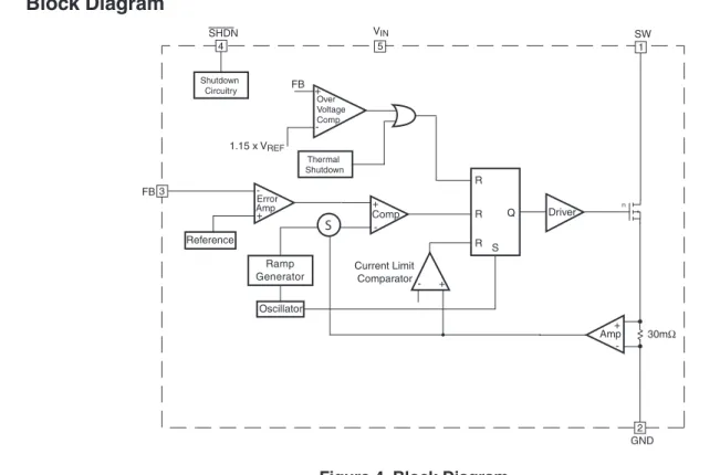
Block Diagram
Figure 4. Block Diagram
Circuit Description
The FAN5333A/FAN5333B is a pulse-width modulated (PWM) current-mode boost converter. The FAN5333A/FAN5333B improves the performance of battery powered equipment by signif-icantly minimizing the spectral distribution of noise at the input caused by the switching action of the regulator. In order to facilitate effective noise filtering, the switching frequency was chosen to be high, 1.5MHz. The device architecture is that of a current mode controller with an internal sense resistor connected in series with the N-channel switch. The voltage at the feedback pin tracks the output voltage at the cathode of the external Schottky diode (shown in the test circuit). The error amplifier amplifies the difference between the feedback voltage and the internal band-gap reference. The amplified error voltage serves as a refer-ence voltage to the PWM comparator. The inverting input of the PWM comparator consists of the sum of two components: the amplified control signal received from the 30mΩ current sense resistor and the ramp generator voltage derived from the oscilla-tor. The oscillator sets the latch, and the latch turns on the FET switch. Under normal operating conditions, the PWM compara-tor resets the latch and turns off the FET, thus terminating the pulse. Since the comparator input contains information about the output voltage and the control loop is arranged to form a negative feedback loop, the value of the peak inductor current will be adjusted to maintain regulation.
Every time the latch is reset, the FET is turned off and the cur-rent flow through the switch is terminated. The latch can be reset by other events as well. Over-current condition is moni-tored by the current limit comparator which resets the latch and turns off the switch instantaneously within each clock cycle.
Over-Voltage Protection
The voltage on the feedback pin is sensed by an OVP Compar-ator. When the feedback voltage is 15% higher than the nominal voltage, the OVP Comparator stops switching of the power tran-sistor, thus preventing the output voltage from going higher.
Open-circuit protection
As in any current regulator, if the feedback loop is open, the out-put voltage increases until it is limited by some additional exter-nal circuitry. In the particular case of the FAN5333, the output voltage is limited by the switching transistor breakdown at around 45V, typically (assuming that COUT and the Schottky diode rating voltage are higher). Since at such high output volt-age the output current is inherently limited by the discontinuous conduction mode, in most cases, the switching transistor enters non-destructive breakdown and the IC survives.
However, to ensure 100% protection for LED disconnection, we recommend limiting VOUT with an external Zener diode or stop-ping the boost switching with an external voltage supervisory circuit.
Applications Information
Setting the Output Current
The internal reference (VREF) is 110mV (Typical) for FAN5333A and 315mV (Typical) for FAN5333B. The output current is set by a resistor divider R connected between FB pin and ground. The output current is given by
Reference Oscillator n FB FB Amp Driver Comp -+ + S Ramp Generator R R R Q S Current Limit Comparator 30mΩ 1.15 x VREF Shutdown Circuitry Thermal Shutdown SHDN GND SW VIN Amp Error 4 5 1 2 3 + Over Voltage Comp + -+ -ILED VFB R ---=
F
AN5333A/F
AN5333B High Efficienc
y
, High Current Serial LED Driver with 30V Integrated Switc
h
Inductor Selection
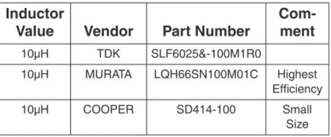
The inductor parameters directly related to device performances are saturation current and dc resistance. The FAN5333A/ FAN5333B operates with a typical inductor value of 10µH. The lower the dc resistance, the higher the efficiency. Usually a trade-off between inductor size, cost and overall efficiency is needed to make the optimum choice.
The inductor saturation current should be rated around 1A, in an application having the LED current near the maximum cur-rent as indicated in “Typical Performance Characteristics”. The peak inductor current is limited to 1.5A by the current sense loop. This limit is reached only during the start-up and with heavy load condition; when this event occurs the converter can shift over in discontinuous conduction mode due to the auto-matic turn-off of the switching transistor, resulting in higher rip-ple and reduced efficiency.
Some recommended inductors are suggested in the table below:
Table 1: Recommended Inductors
Capacitors Selection
For best performance, low ESR input and output capacitors are required. Ceramic capacitors of CIN = 10µF and COUT = 1µF placed as close to the IC pins, are required for the maximum load(65mA). For the lighter load (≤ 20mA) the capacitances may be reduced to CIN = 4.7µF and COUT = 0.47µF or even to 0.1µF, if higher ripple is acceptable. The output capacitor voltage rating should be according to the VOUT setting.Some capacitors are suggested in the table below.
Table 2: Recommended Capacitors
Diode Selection
The external diode used for rectification is usually a Schottky diode. Its average forward current and reverse voltage maxi-mum ratings should exceed the load current and the voltage at the output of the converter respectively. A barrier Schottky diode such as BAT54 is preferred, due to its lower reverse current over
Brightness Control
1. Dimming Using PWM Logic Signal
A PWM signal applied to SHDN Table 5 on page 8 can control the LED’s brightness in direct dependence with the duty cycle. The maximum frequency should not exceed 1kHz to ensure a linear dependence of the LED’s average current. The amplitude of the PWM signal should be suitable to turn the FAN5333 ON and OFF.
Alternatively, a PWM logic signal can be used to switch a FET ON/OFF to change the resistance that sets the LED’s current Table 6 on page 8. Adjusting the duty cycle from 0% to 100% results in varying the LED’s current between IMIN and IMAX. Where
Figure 5. Dimming Using a PWM Signal
Figure 6. Dimming Using a PWM Logic Signal
2. Dimming Using DC Voltage
An external adjustable DC voltage Table 7 on page 8 between 0V to 2V can control the LED’s current from 15mA to 0mA, respectively.
Figure 7. Dimming Using DC Voltage
Inductor
Value
Vendor
Part Number
Com-ment
10µH TDK SLF6025&-100M1R0 10µH MURATA LQH66SN100M01C Highest Efficiency 10µH COOPER SD414-100 Small SizeCapacitor
Value
Vendor
Part Number
0.47µF Panasonic ECJ-3YB1E474K 1µF Murata GRM21BR61E105K 10µF Murata GRM21BR61A106K IMIN VFB RMIN ---= and IMAX VFB RMIN RSET ---= SHDN FAN5333 FB FAN5333 RMIN RSET FB VDC 90KΩ 5Ω 1.6KΩ FAN5333A FB VDC 90KΩ 15Ω 4.7KΩ FAN5333B
F
AN5333A/F
AN5333B High Efficienc
y
, High Current Serial LED Driver with 30V Integrated Switc
h
3. Dimming Using Filtered PWM Signal
This method allows the use of a greater than 1kHz PWM fre-quency signal with minimum impact on the battery ripple. The filtered PWM signal Table 8 on page 9 acts as an adjustable DC voltage as long as its frequency is significantly higher than the corner frequency of the RC low pass filter.
Figure 8. Dimming Using Filtered PWM Signal
Thermal Shutdown
When the die temperature exceeds 150°C, a reset occurs and will remain in effect until the die cools to 130°C, at that time the circuit will be allowed to restart.
PCB Layout Recommendations
The inherently high peak currents and switching frequency of power supplies require careful PCB layout design. Therefore, use wide traces for high current paths and place the input capacitor, the inductor, and the output capacitor as close as possible to the integrated circuit terminals. The FB pin connec-tion should be routed away from the inductor proximity to pre-vent RF coupling. A PCB with at least one ground plane connected to pin 2 of the IC is recommended. This ground plane acts as an electromagnetic shield to reduce EMI and parasitic coupling between components.
FB 20KΩ 15KΩ 5Ω 1.6KΩ FAN5333A 0.1µF FB 20KΩ 15KΩ 15Ω 4.7KΩ FAN5333B 0.1µF
F
AN5333A/F
AN5333B High Efficienc
y
, High Current Serial LED Driver with 30V Integrated Switc
h
Mechanical Dimensions
5-Lead SOT-23
Ordering Information
Symbol
Inches
Millimeters
Notes
Min
Max
Min
Max
A .035 .057 .90 1.45 A1 .000 .006 .00 .15 B .008 .020 .20 .50 c .003 .010 .08 .25 D .106 .122 2.70 3.10 E .059 .071 1.50 1.80 e .037 BSC .95 BSC e1 .075 BSC 1.90 BSC H .087 .126 2.20 3.20 L .004 .024 .10 .60 0º 10º 0º 10º
Product Number
Package Type
Order Code
FAN5333A 5-Lead SOT23 FAN5333ASX
FAN5333B 5-Lead SOT23 FAN5333BSX
D e1 e B E H A A1 α L c α
F
AN5333A/F
AN5333B High Efficienc
y
, High Current Serial LED Driver with 30V Integrated Switc
h
DISCLAIMER
FAIRCHILD SEMICONDUCTOR RESERVES THE RIGHT TO MAKE CHANGES WITHOUT FURTHER NOTICE TO ANY PRODUCTS HEREIN TO IMPROVE RELIABILITY, FUNCTION OR DESIGN. FAIRCHILD DOES NOT ASSUME ANY LIABILITY ARISING OUT OF THE APPLICATION OR USE OF ANY PRODUCT OR CIRCUIT DESCRIBED HEREIN; NEITHER DOES IT CONVEY ANY LICENSE UNDER ITS PATENT RIGHTS, NOR THE RIGHTS OF OTHERS.
TRADEMARKS
The following are registered and unregistered trademarks Fairchild Semiconductor owns or is authorized to use and is not intended to be an exhaustive list of all such trademarks.
LIFE SUPPORT POLICY
FAIRCHILD’S PRODUCTS ARE NOT AUTHORIZED FOR USE AS CRITICAL COMPONENTS IN LIFE SUPPORT DEVICES OR SYSTEMS WITHOUT THE EXPRESS WRITTEN APPROVAL OF FAIRCHILD SEMICONDUCTOR CORPORATION. As used herein:
1. Life support devices or systems are devices or systems which, (a) are intended for surgical implant into the body, or (b) support or sustain life, or (c) whose failure to perform when properly used in accordance with instructions for use provided in the labeling, can be reasonably expected to result in significant injury to the user.
2. A critical component is any component of a life support device or system whose failure to perform can be reasonably expected to cause the failure of the life support device or system, or to affect its safety or effectiveness.
PRODUCT STATUS DEFINITIONS Definition of Terms
Datasheet Identification Product Status Definition
Advance Information
Preliminary
No Identification Needed
Obsolete
This datasheet contains the design specifications for product development. Specifications may change in any manner without notice.
This datasheet contains preliminary data, and supplementary data will be published at a later date. Fairchild Semiconductor reserves the right to make changes at any time without notice in order to improve design.
This datasheet contains final specifications. Fairchild Semiconductor reserves the right to make changes at any time without notice in order to improve design.
This datasheet contains specifications on a product that has been discontinued by Fairchild semiconductor. The datasheet is printed for reference information only. Formative or In Design First Production Full Production Not In Production