A basic introduction to
Cadence OrCAD PCB Designer
Version 16.3
Professor John H. Davies
Department of Electronics and Electrical Engineering
Glasgow University, Glasgow, G12 8QQ, Scotland, UK
Email:
[email protected]
2011 October 6
Contents
Preamble 2
1 Introduction 3
2 One-transistor amplifier: Schematic capture 5
3 OrCAD PCB Editor 14
4 Instrumentation amplifier – single-sided board 25
5 Instrumentation amplifier – double-sided board 35
6 Artwork and drill files 39
7 Summary: PCB design flow 46
A Where to learn more 47
B Capture techniques 50
C PCB Editor techniques 51
D PCB Router techniques 65
Preamble
This document introduces the basic features of OrCAD PCB Designer. It is aimed primarily at novices with limited experience of construction who have never designed a PCB before. For this reason I concentrate on pin-through-hole devices (although surface-mount devices are no more difficult) on single and double-sided boards. I strongly recommend Mitzner’s book [1] instead if you are an experienced designer, interested in more advanced PCBs for commercial production.
Other readers may be experienced users of OrCAD Layout who are obliged to switch to PCB Editor; I hope that they don’t feel that their intelligence is insulted! I’ve highlighted some of the most significant differences between Layout and PCB Editor. (I think that PCB Designer refers to the complete suite while PCB Editor is the specific application for editing PCBs but it’s not entirely clear.)
I adapted this document from an introductory class and have removed several features that are unlikely to be of interest to most readers. For example, we have developed a local library of footprints for PCBs constructed by students. The pads are enlarged to allow easy soldering and the symbols contain features to discourage common design errors, such as tracks to inaccessible pads underneath connectors. However, I’ve retained the instructions to produce photomasks directly with the Plot command, rather than with Gerber files. This is helpful if you make PCBs in-house by traditional processes, which is often the case for student projects.
Differences between versions 16.0, 16.2 and 16.3
Version 16.3 of OrCAD was released in late 2009, following 16.2 in late 2008. TheWhat’s New document exceeds 90 pages but most of the changes aren’t relevant to an introductory tutorial. Here are the most important new features in version 16.2.
• The appearance of Capture has been updated to match PCB Editor. Buttons are now larger and their purpose is sometimes clearer. A bar of tabs can be used to switch between windows.
• Cross-probing between Capture and PCB Editor has been improved.
• The Plot command can leave drill holes open, which may be helpful for PCBs drilled by hand.
• The software is installed in the same way, regardless of whether you have a licence or not. Applications simply run in demonstration mode if they cannot find a licence. The demo version is a great improvement on previous editions but the installer has a peculiarity: you are forced to specify a licence server even if you wish to use only the demo mode. A bogus server such as5280@localhostshould get around this problem.
This tutorial is affected less by changes from 16.2 to 16.3.
• A board can now be ‘flipped’ (viewed from underneath rather than from the top) and rotated in 3D but this is of limited value for the simple designs described here.
• The autorouter is now called Allegro (or OrCAD) PCB Router rather than SPECCTRA. Board files written by version 16.3 of PCB Editor cannot be read by version 16.2, nor can those written by 16.2 be read by version 16.0. (This contradicts the statement inGetting Started with Physical Designthat ‘Allegro PCB Editor databases are backward-compatible with their major version number (the number to the left of the dot)’.) Use the menu itemFile > Export > Save design to 16.2. . . (or16.01. . .) to write a file compatible with an earlier version. (The jargon is todownrevthe design.) I have not yet updated this document for version 16.5.
Prospectus
This document falls into two major parts.
• The main body is a tutorial that guides you through the layout of two simple PCBs. First is a one-transistor amplifier, which is really straightforward but allows you to concentrate on the interface of the applications. The second design is an instrumentation amplifier, which is laid out on single and double-sided PCBs using the autorouter. I also show how to produce manufacturing data for this design.
• The appendices contain a collection of techniques that you might find useful. Links to these are given in the tutorials.
PCB Editor has so many features, even in its OrCAD version, that I cover only a small fraction of them.
1
Introduction
The Cadence OrCAD PCB Designer suite comprises three main applications.
• Capture is used to draw the circuit on the screen (schematic capture). Anetlist, which describes the components and their interconnections, is the link to PSpice and PCB Edi-tor.
• PSpicesimulates a captured circuit. I do not describe PSpice in this tutorial.
• PCB Editor (Allegro)is the application for laying out a printed circuit board. It includes an automatic router that works out the arrangement of tracks needed to connect the com-ponents on the PCB. The output from PCB Editor is a plot or a set of files that can be sent to a manufacturer.
The overalldesign flow for making a PCB is shown in figure 1 on the following pagewith a summary in section7 on page 46.
PCB Editor replaces the earlier application, Layout, which is now discontinued. OrCAD PCB Designer is the most basic version of Cadence’s Allegro suite for PCB design and much of the documentation refers to ‘Allegro’ rather than ‘PCB Editor’.
Fixup. The libraries for Capture and PCB Editor have some incompatibilities that must be corrected byFixups. I hope to find smoother ways around these difficulties in the future.¦
Capture PCB Editor Draw schematic Add footprints Create netlist
Set up bare board (outline, design rules)
Engineering Change Order (ECO)
Place and arrange
components Export to PCB Router Return to PCB Editor Route board automatically Spread and mitre tracks Route board automatically Gloss board Route board manually
Annotate and print board Libraries PCB Router Check placement of vias netrev
Figure 1. Design flow for making a PCB with Capture and PCB Editor. The three paths for PCB Editor depend on whether the tracks are drawn manually (as in the first design), automat-ically within PCB Editor, or by running the autorouter as a separate application.
1.1
Libraries, files, directories and design rules
Three types of information are needed for each component, corresponding to the three main applications listed above.
• Electrical symbolsare used to draw the circuit in Capture.
• Electrical modelsallow you to simulate the circuit in PSpice.
• Footprints orpackage symbols show the physical size and shapes of the pads (where the pins are soldered to the board) and the outline of the package. They are used to lay out the circuit in PCB Editor.
These are stored in different sets of libraries and you must select the files needed for a particular design. Footprints are needed as well as electrical symbols because components with the same electrical behaviour come in different packages. For example, an integrated circuit might come in two versions:
• a smaller, surface-mount device (SMD) with pins only 0.5 mm apart, if it has pins at all The opposite is also true: resistors of a particular shape come in a wide range of values.
Further information is needed to describe the characteristics of the printed circuit board on which the components are mounted. The details are important for high-speed designs but we need to know only the number of layers of copper, calledetchin PCB Designer. This tutorial covers only single-sided boards, which have components on top and copper on the bottom, and double-sided boards, which have copper on both surfaces but usually components only on the top. Fancier boards often have two internal planes of copper used for power and ground; complex designs need further layers.
Design rulesare required to lay out the circuit on the PCB. The full details are complex but the basic rules specify the minimum width of tracks and the gap between them. Manufacturers often express these numbers in the format 10/8, meaning minimum widths of 10 for tracks and 8 for gaps (although the numbers are usually the same). The units are almost alwaysmils, which mean thousands of an inch; see section2.5 on page 10. I use 25/25 rules in this tutorial, which are extremely coarse but produce boards that are easy for inexperienced students to solder.
Further design rules control a diverse range of features, such as the spacing between tracks and pads, whether vias are permitted and the impedance of tracks (they act like transmission lines at high frequency). These rules are adjusted with the Constraint Manager, which we’ll encounter in section4.4 on page 29.
Fixup. Older versions of OrCAD prefer designs to be stored inOrCAD_Datarather thanMy Documentsand may reject filenames that contain spaces. If you get inexplicable errors about unexpected arguments or incomplete file names, try copying the design toOrCAD_Data and removing spaces from the names of all directories and files. ¦
1.2
Help!
All programs provide extensive online help. AppendixA on page 47 explains how to use the Cadence Help system and guides you around the major documents supplied with PCB Designer. Many commands in PCB Editor have names that are not obviously related to the corresponding item on the menus so I have pointed these out.
2
One-transistor amplifier: Schematic capture
The first design is a one-transistor amplifier. It has only a few components and will be laid out on a huge board to make the routing straightforward: The challenge is to learn the software. The initial step is to draw the circuit in Capture.
Capture treats each circuit design as a project and a project manager shows the logical relation between the files required. It is essential to create a new directory for each project. Strange errors can occur if you have more than one project in a directory, from which it seems impossible to recover. It also keeps your work organised. OrCAD creates a subdirectory for PSpice files and an allegro subdirectory for PCB files. You should know this by now but a reminder is never a bad idea: Save your work frequently and take regular backups of important circuits.
Note. I have wasted hours trying to reconstruct projects where students have not obeyed the rule of one project per directory! I don’t know why they find it so difficult.¦
Select Start > Programs > OrCAD 16.2 > OrCAD Capture. I use ‘>’ throughout this document to show the levels of a hierarchical menu. There will be a short delay while the software is loaded and the licence server is accessed. Alternatively, you will be asked if you wish to use Demo mode if no licence can be found. The screen then shows the OrCAD Capture main window with a menu bar and various toolbars. A sub-window at the bottom shows the session log; its title may be hard to find if the window has been docked. Version 16.3 offers different ways of controlling the windows; right-click in a title bar.
2.1
Create a project
The first step in OrCAD is always to create a project.
1. Create a new directory in Windows to hold all files for the project. 2. SelectFile > New > Projectfrom the menu bar of Capture.
3. In theNew Projectdialog box:
• Select anAnalog or Mixed A/Dproject if you wish to simulate the circuit. You could use thePC Board WizardorSchematicoptions if you don’t want to simulate the circuit, in which case the steps differ slightly from my description.
• Click on theBrowsekey and navigate to the new directory that you created for this design. ClickOK.
• Give the project a meaningful name.
• The path and directory now show in the location box (if you can see them – they are usually too long). ClickOKin the New Project dialog box.
• ClickNext.
4. Select theCreate a blank project button in the small dialog box that appears and click
OK.
5. Your project will now be created. The Project Manager window at the top left shows the files associated with your design and the resources used, such as library files. Its title is the full pathname of your project, which is usually far too long to fit. Make theFiletab active if necessary.
6. Expand the Design Resources folder in the project, then the design (called ./project-name.dsn, where project-name is the name of your project), then the SCHEMATIC1
folder and finally double-clickPAGE1to open the schematic page for your design. Lo-cate the Title box in the lower right-hand corner, double-click on the placeholders, which are in angle brackets<>, and replace them with a descriptive title and so on.
+10V Gnd Gnd Output Input J2 Output J2 Output 1 2 3 R2 2.7k R2 2.7k R3 390 R3 390 C2 100u 16V C2 100u 16V 1 2 Q1 BFY51 Q1 BFY51 J1 Input J1 Input 1 2 R4 180 R4 180 C1 1u C1 1u R1 7.4k R1 7.4k
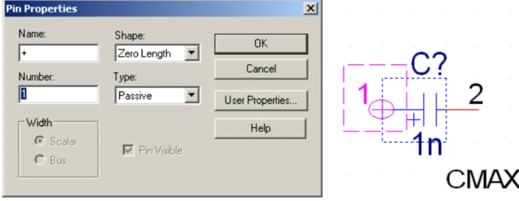
Figure 2. Schematic drawing of a simple, one-transistor amplifier. The pin numbers on the electrolytic capacitor are not normally visible but are shown to illustrate a fixup later.
2.2
Draw the circuit
Draw the circuit shown in figure2. The names of the components are listed in table1 on the following page; I’ve renamed some of them to make their functions clearer. I assume that you are familiar with Capture but here are a few tips to help.
Jargon: The label that identifies each component on the schematic drawing is called its refer-enceorrefdes, short forreference designator. For example, the transistor has refdes Q1. Each refdes must be unique: No other component can be called Q1.¦
• I used libraries from the pspice folder so that the circuit could be simulated although I do not describe that here. Basic components like resistors are in the analog library. The connectors are in theconnector library, which is in the directory one level above thepspicedirectory (OrCAD16.3/tools/capture/library/). UseSearchif you can’t guess where a component is located. You may need to do this for the transistor.
If you have no intention of simulating the circuit you might prefer to use components from thediscretelibrary instead ofpspice/analog. This avoids a problem with the num-bering of pins that will arise shortly.
• The capacitorC2is anelectrolytictype, which must be installed with the correct polarity or it will explode. One of its plates on the schematic is therefore labelled with a+sign and must be connected to a positive voltage. (Its pin numbers are also shown because of a fixup later.) The parameter CMAXis the maximum working voltage of the capacitor, which is not needed for simulation but important when you pick out the real component. I set it to 16 V, which is a common value.
• Always join components with wires, not by placing them so close that their pins overlap. This can cause strange errors.
Table 1. Components, names in Capture and footprints for the one-transistor amplifier. These are taken from the library supplied with PCB Designer. The names are not case-sensitive.
Part Capture name Footprint name
Resistors R res400
Capacitor, non-polarised C cap600 Capacitor, electrolytic C_elect cap196 Connector, input HEADER 2 jumper2 Connector, output and power HEADER 3 jumper3
Transistor BFY51 to5 (letter ‘oh’ not number zero)
• Wires and components sometimes become joined incorrectly if you move them about. Use Place > Junction or the junction tool from the toolbar on the right to eliminate spurious connections.
• Include connectors for all wires that leave the PCB. This includes inputs, outputs and the power supplies. It is a good idea to change the ‘values’ of connectors to make them more descriptive than the defaults, for exampleInputrather thanHEADER 2. Do not edit the reference, such asJ1.
• Add text to label the pins of each connector.
Print the drawing sheet: You will need this soon to guide the layout of your PCB. This circuit takes up only a small part of the page so it is a good idea to chooseFile > Print Area > Setand mark out a rectangle that includes only the part of the page that you wish to print. Check the circuit carefully– it is much easier to correct mistakes at this stage.
Note. ThePlace Partdialog box is a pop-out panel in version 16.3 and its appearance has been modified considerably from the traditional version. The functionality is unchanged. Click on the ‘pin’ icon in the title bar to fix it if you prefer.
Some students change theReference(J1orJ2) of the connectors toInputorOutputinstead of changing theValue(HEADER 2orHEADER 3). This upsets the netlister later.¦
2.3
Preparation for PCB layout
The procedure to this point should be familiar if you have used Capture with PSpice. A few extra steps are needed to prepare the schematic for a PCB.
Fixup. The electrolytic capacitorC_elect in the pspice/analog library is incompatible with its footprint. The pins of the footprint are numbered 1, 2 but those of the capacitor are p, n. This means that the software cannot match the capacitor to its footprint. Edit the electrolytic capacitor and change the numbers of its pins to resolve this.
1. Select the electrolytic capacitor and chooseEdit > Part from the menu bar. A window opens with an enlarged view of the capacitor.
Figure 3. Edit Part window and Pin Properties dialogue box for correcting the numbering of the pins of the electrolytic capacitor.
2. The positive pin is shown as a circle on the left. Select it and and chooseEdit > Proper-ties. . .. This brings up the Pin Properties dialogue box, shown in figure3.
3. Change theNumberto1and clickOK. Don’t worry about the name of the pin. 4. The negative pin is shown as a red line on the right. Change itsNumberto2.
5. Choose File > Close. You have the choice of updating this part alone, or all ‘part in-stances’ – that means all C_elect components in your design. There is only one so it doesn’t matter whether you chooseUpdate CurrentorUpdate Allin this case.
I made the pin numbers visible for the electrolytic capacitor in figure2 on page 7as a reminder of this fixup. You need not do this.¦
This problem can be avoided by using components from thediscretelibrary instead, which is in the directory one level above the pspice directory. However, these components are not associated with pspice models and therefore cannot be used for simulation.
The main task in preparing the design for layout is to associate afootprintwith each com-ponent. The footprint shows the physical outline of the components including the copperpads to which the pins are soldered. Most pads are either circular or oval except for pin 1, which has square corners to identify it. The components in many Capture libraries have footprints already but unfortunately they are mostly wrong. We must therefore enter the correct footprints, which are listed in table 1 on the previous pagefor this circuit. Don’t muddle the letter ‘o’ with the numeral ‘0’. The whole business of assigning footprints is unnecessary if you have a database of components in Capture CIS.
1. Drag the cursor over your schematic drawing so that all the components are enclosed in a rectangle. Do not include the title box.
2. ChooseEdit > Properties. . . from the menu bar, which brings up the Properties spread-sheet.
3. Type each name into the PCB Footprint field of the Properties spreadsheet. All the resistors have same footprint so use copy and paste for speed.
Faster methods of entering identical footprints are described in sectionB on page 50.
Tip for Layout users: PCB Designer comes with a small library of footprints compared with the extensive libraries that were provided with Layout. I’ve been told that this is because most users have their own libraries. Where there is a need, somebody will offer a service: Online libraries of footprints are available – for a fee.
PCB Editor has no convenient way of copying the names of footprints into Capture from a library, as in Layout. I describe a feeble substitute in sectionC.12 on page 64. PCB Editor also lacks anything like the library manager in Layout. ¦
2.4
Design rules check
The next step is a Design Rules Check to ensure that no errors have been introduced.
1. Click on the Project Manager window and highlight your design (with extension.dsn). 2. SelectTools > Design Rules Check. . . from the menu bar.
3. UnderDesign Rules select both Run Electrical Rules (probably selected already) and
Run Physical Rules(probably not).
4. ClickOK. A dialog box may reportOne or more errors or warnings were encountered. Do you wish to view the messages in the session log? Agree to this and review the report in theSession logwindow. No positive message is given to confirm that all rules have been passed successfully, just an absence of complaints. Ask for help if you do not understand a message– don’t just ignore it.
5. Return to your drawing and correct any errors, shown by green circles (a strange choice of colour). Repeat until the Design Rules Check runs silently.
6. You may wish to run the Design Rules Check and selectAction > Delete existing DRC markersto get rid of the green circles. They do not vanish by themselves.
2.5
Make a bare board in PCB Editor
The simplest way of creating a PCB is first to set up an empty PCB, then to add your compo-nents and connections to the board. This follows the design flow shown in figure1 on page 4. See section C.2 on page 53 for a more conventional flow where you make the netlist before defining the board.
First create a directory allegro within your directory for the current project. PCB Editor likes to keep its files here. ChooseStart > Programs > OrCAD 16.3 > OrCAD PCB Editor, which opens theOrCAD PCB Designerapplication (Cadence seem muddled about the name). I’ll leave the details of the interface until later because we need only one dialogue box for this step.
ChooseFile > New. . . from the menu. In the first dialogue box, set theDrawing Type to
Board (wizard). ClickBrowse. . ., navigate to your newallegrodirectory and give the board a name such asbare.brd. ClickOpenthenOKto bring up the new board wizard. This takes you
through several screens to define the parameters of the PCB. Some of these are obvious, such as the size of the board, while others set up thedesign rules – the width of tracks on the PCB, how much space must be left between them, and so on.
1. The first screen is purely descriptive. Read it, then clickNext >.
2. This asks for a board template. We don’t have one so selectNo(probably the default) and clickNext >.
3. You are next asked for a ‘tech’ file. This is short for atechnologyfile, which specifies the design rules. Again we don’t have one so selectNoand clickNext >.
4. This asks for a board symbol. SelectNoagain and clickNext >.
5. We now reach the screens for the parameters that must be set up. The units should be Mils. These are not millimeters but the American term for thousandths of an inch; 1 mm≈40 mils. All dimensions are given in these units so get used to them.
Leave the drawing size atA. This is an American size but you aren’t allowed European A4 if the units are mils. Leave the origin at the centre.
6. Set the grid spacing to be 100 mils.
TheEtch layer countis the number of copper layers on the board – the number of layers of tracks for signals and power. Leave this at 2, although we shall use only one layer in the first design.
SelectGenerate default artwork films, which is the default.
7. Leave the names of the layers asTopandBottomand their types asRouting Layer. 8. Enter 25 for the Minimum Line width (in mils). This value propagates into the other
boxes. It means 0.02500 or about 0.64 mm, which is very wide for a track nowadays but makes the board easy to solder by hand.
For theDefault via padstack, click on the button with. . . and chooseVia26. This design is far too simple to need vias, which carry a signal from one layer of the PCB to another, but they may be required later.
9. Rectangular board (it’s curious that a circular board is the default).
10. Enter a width of 3000 and height of 2000 mils. This defines the board outline as 300×200. There is no corner cutoff.
Specify theRoute keepin distance as 100. Akeepin means that objects must be kept inside the specified region. In this case it means that tracks cannot go any closer than 100 mils to the edge of the board. It gives a border around the PCB to aid handling and manufacture. (We’ll encounter keepouts as well later.)
Set thePackage keepin distanceto 250. Components must be placed within this keepin and therefore cannot be closer than 250 mils to the edge of the board. The gap between the two keepins allows you to run tracks around the outside of all the components, which is often helpful on a more complicated board (although hardly necessary here).
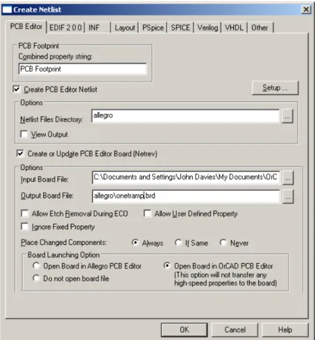
Figure 4. Completed dialogue box for netlisting the design and sending it to PCB Editor. Your file names will be different.
11. ClickFinish– that’s it.
This has set up the design rules and made an empty board, which you can see in the design window of PCB Editor, shown in figure5 on page 15. Three rectangles are visible for the board outline, route keepin and package keepin. ChooseFile > Saveand close PCB Editor.
The next step is to return to Capture and send the circuit to PCB Editor so that it can be added to the bare board.
Tip for Layout users: PCB Designer does not come with a library of technology files, as did Layout. Cadence expect you to have your own. Fortunately it is easy to export a tech file from a board file that you have set up to your liking; see sectionC.4 on page 54. ¦
2.6
Create a netlist
The information about your design is sent from Capture to PCB Editor in the form of anetlist, which contains a description of the circuit and its components. (The netlist comprises three files but you rarely need to look at them.)
1. Highlight your design (the object whose name ends in .dsn) in the Project Manager window of Capture.
2. SelectTools > Create Netlist. . . from the menu bar, which brings up the dialogue box in figure4 on the preceding page. Make sure that thePCB Editortab is active.
3. Confirm that the PCB Footprint box containsPCB Footprintand that the box underneath forCreate PCB Editor Netlistis selected.
4. Under Options, the Netlist Files Directory should be shown asallegro. Select Create or Update PCB Editor Board (Netrev). Netrevis the application that merges the netlist, footprints and other information into the database used by PCB Editor, hence its central position in figure1 on page 4.
5. ForInput Board File, choose the bare board that you have just set up. Click on the ‘. . .’ button to navigate.
6. TheOutput Board Fileusually shows something sensible automatically; edit it if not. It should use the newallegrodirectory.
7. UnderBoard Launching Option, select Open Board in OrCAD PCB Editorif your li-cence doesn’t cover the full version of Allegro.
8. The entries in the dialogue box should now resemble figure4 on the preceding page ex-cept exex-cept for the pathnames. ClickOKto dismiss this dialog box and start the netlister. You are warned that your design will be saved by Capture, then a Progress box shows the various processes needed: Netlisting the design followed by Updating OrCAD PCB Editor Board. PCB Editor is then launched with your new board.
• You may see a Warning box, which tells you that Netrev succeeded with warnings. Check the Session Log if this happens. Messages about RVMAX and CMAX can be ignored; these are maximum voltage ratings of the components and are not important for this circuit.Pay attention to any others!
• OrCAD PCB Editor gives you a warning thatDatabase was last saved by a higher tier tool, which you can ignore.
You should now see your empty board outline on the screen of PCB Editor again; the compo-nents have been added to the database but are not yet visible.
Note. The netlister in some versions of 16.x has a nasty bug (the pxllite bug). The symptoms are that the Netlist Files Directory does not show as allegro automatically in figure 4 on the previous page and that nothing happens when you run the netlister – not even an error mes-sage. Netlisting for PCB Editor must be performed once on each computer by a user with administrator privileges before it will work for anybody else.
PCB Editor is almost always launched even if there was a fatal error during netlisting: It is vital to check the session log. Many students don’t bother, and discover only later that components are missing.
Check the search paths if PCB Editor complains that it can’t find components. This shouldn’t occur if you use the standard libraries but may arise with local libraries. ChooseSetup > User Preferences. . . from the menu bar, which brings up the User Preferences Editor, then look at Design_paths in the list of Categories.¦
Tip for Layout users: This process is similar to creating a netlist in Layout – it just uses a different tab in theCreate Netlistdialogue box.
Where are my components?Layout automatically displays the components on screen, ready for you to move on the PCB. Allegro does not do this: You must place them yourself. The
Quickplacecommand, which I’ll describe in section4.2 on page 28, achieves the same effect as Layout.¦
3
OrCAD PCB Editor
The interface of PCB Editor may feel unfamiliar because the application was originally devel-oped for unix and has been ported to Windows with minimal changes. Some distinctive features are obvious almost immediately.
• The design window, which shows your board, has no scroll bars.
• One design is always open; you cannot open more than one, nor close the current design without opening a new one or exiting the application.
• There is no ‘null’ tool, such as the pointer shown by most drawing applications when no other tool is selected.
An important aspect of the interface is that tools can be used in two ways.
• First choose a command, either from the menu bar or by clicking a button, then the element of the design on which the tool should operate.
• Select the object first, then the command from the contextual menu by right-clicking. I shall use both methods in the tutorials, picking whichever seems most natural at the time. However, confusion can arise when you change from one method to the other. It is therefore a good idea when switching to disable any active tool (right-click and chooseDoneif it is offered) and clear any selection (left-click outside the board or right-click and chooseSelection Set > Clear All Selections). See sectionC.1 on page 51for a fuller description of the user interface.
3.1
The screen
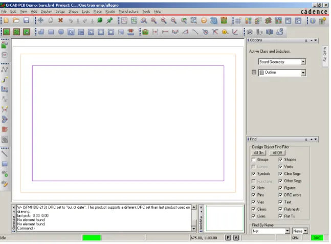
PCB Editor needs a big screen – the elderly laptop that I have used to illustrate these instructions is not large enough to show all the toolbars! The main elements of the application are shown in figure5 on the following page.
• Design window, occupying most of the screen, where you lay out the PCB. It always shows the board viewed from the top; the bottom layer is seen through the board as if it were transparent.
Figure 5. Screenshot of OrCAD PCB Editor with an empty board; the black background has been changed to white for a clearer printout. The rectangles show the board outline (outer), route keepin and package keepin (inner). The Find and Options control panels have been pinned open on the right.
• Menu baralong the top as usual.
• Toolbarsin two rows under the menu bar and a further column down the left-hand side. Their arrangement depends on the size of the screen. Hover the pointer over a button to reveal its function.
• Control panelswith tabs on the right-hand side. Each panel pops out when you move the pointer over its tab. Click the pin to lock a panel open.
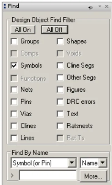
– Findselects the type of object that is highlighted when you move the mouse around the drawing.
– Optionschanges according to the current mode and command; it selects the active class and subclass when PCB Editor is idle, then offers appropriate options when a command is chosen.
– Visibilityhides layers of etch while routing the board; predefined settings select the films of artwork that will be used to manufacture the PCB.
I strongly recommend that you keep the Find and Options panels pinned open as in figure
• Command console window at the bottom left of the screen. This prints a running log of your actions and is useful to show when Allegro is waiting for input from you. It also displays the output from commands such as Design Rules Check.
• Worldview windowat bottom right shows how the relation between the board outline and the view in the design window. It is useful for moving the design window around the board as we shall soon see.
• Status barat the bottom of the screen. It shows the coordinates of the pointer (crosshairs). TheP(Pick) button is useful for typing coordinates instead of clicking with the mouse if your hand is unsteady.
At the far right is a coloured block calledDRC, which stands for Design Rules Check. It may be yellow because checking is not up to date. Usually it should be green to show that automatic checking is turned on and that no errors are detected.
A lot of jargon is associated with Allegro. It often refers to your design as thedatabase, because that’s what it is from the point of view of the computer. The various elements of the design are classified intoclassesandsubclasses, which I’ll write asclass/subclassin the instructions. Here are some common examples.
• TheEtchclass includes the regions of copper that act as pads for the components and the tracks that carry the signals between them. The simple designs described here have two subclasses of etch, Top and Bottom. They are coloured green and yellow respectively by default.
• The Board Geometry class includes the Outline, which we have already seen. Sub-classesSilkscreen_BottomandSilkscreen_Topare used for text to annotate the board. • We have also seen thePackage Keepinclass, used to prevent components being placed
too close to the edge of the board. It has no subclasses.
The class and subclass can be chosen in the Options control panel but PCB Editor usually selects them automatically when you make a tool active.
Tip for Layout users:The colours used by PCB Editor are different from those used by Layout but can be changed if you wish with the Color Dialog, described in section6.1 on page 39. ¦
3.2
Moving around the design
Two methods can be used topanorroamaround the design – move the display to the region of interest.
• Use the arrow keys on the keyboard.
• Hold down the middle button of the mouse and drag. A confusing feature of this is that it drags the window over the design. This means that the design moves in theopposite direction to your drag. It is the reverse of the hand ‘grabber’ in applications such as Acrobat, which drag the design under the window.
But I have only a two-button mouse! Many two-button mice have a scroll wheel, which acts as the middle button when pressed.
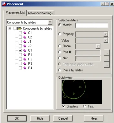
Figure 6. The Placement dialogue box, showing the components for the one-transistor ampli-fier. Transistor Q1 is ready to be placed on the board.
You also need tozoominto the design to concentrate on small details or zoom out to review the complete layout. Again there are two methods.
• Use the commands under the View menu or the corresponding buttons and shortcuts.
Zoom Fitfills the window with your complete design, which is often helpful.
• The scroll wheel of the mouse zooms in and out, centred on the current position of the pointer.
The WorldView window can also be used to zoom and pan. If you drag a rectangle here, that becomes the area shown in the design window.
I could write a lot more about the interface (look at section C.1 on page 51if you want to know) but it is more fun to place the components and route the PCB.
3.3
Place and arrange the components
ChoosePlace > Manually. . . from the menu bar to start placing the components. This brings up the Placement dialogue box shown in figure6. ThePlacement Listtab should be active and the list should showComponents by refdeswith the components in your design listed below. Allegro can place components automatically (not in the OrCAD version) but it is straight-forward to place them manually for this simple design. See figure7 on the following pagefor guidance.
1. Start with the transistor. Click the box next to Q1 in the Placement dialogue. Its outline appears in theQuickviewbox (assuming that Graphics has been chosen).
Figure 7. Screenshot of the board for the simple, one-transistor amplifier after all compo-nents have been placed and arranged. Cyan lines of the ratsnest show the connections between components.
2. Move the cursor out of the Placement box on to your design. The outline of the transistor follows the cursor. Left-click to place it centrally on your board. The outline fills in and a smallPfor ‘placed’ appears in the Placement box next to the refdes.
3. Place the connectors for input and output next. Select the boxes for both J1 and J2. Move the mouse onto the design and a two-pin header for J1 appears on the cursor. Click somewhere near the left-hand side to place it. Don’t worry about its orientation for now. 4. The outline of J2 now appears automatically on the cursor. Place this on the right-hand
side.
5. Next place the four resistors. Put them in the same positions relative to the transistor that they have on your schematic drawing. This makes the circuit easier to wire. Refer to your schematic drawing to identify each resistor.
Keep all components inside the inner purple rectangle, which shows the Package Keepin. It turns green if you try to place any part of a component outside it.
6. Place the two capacitors in the same way. This completes the placement so dismiss the dialogue box.
Note. Components can be selected in Capture for placement in PCB Editor while the Placement dialogue box is open. See sectionC.3 on page 53.
If components are missing, there was probably an error during netlisting. Go back and check the session log in Capture.
Why am I seeing the text double? – and why all the ***? See section C.10 on page 60, which explains the purpose of the text and how to get rid of the surplus.¦
The components are joined by a set of cyan lines called theratsnest to show their logical connections. These lines will be turned into copper tracks when youroutethe board. The lines
Figure 8. TheFindcontrol panel set up so that only symbols can be selected.
of the ratsnest simply take the shortest path between components and therefore cross other lines. Real tracks cannot do this. It is therefore vital to adjust the orientation and position of the placed components to reduce the number of crossings in the ratsnest and make routing easier.
Before doing this, experiment by moving the mouse around the design window without clicking. Elements of the design are highlighted and an explanatory note appears as the mouse passes over; there is no need to click on an object to highlight it as in many drawing programs. If you hover the cursor over the outline of the transistor, for example, the messageComponent Instance "Q1"is shown. The mouse may highlight the outline of a component, its pins, text or lines of the ratsnest. How can we be sure to move acompletecomponent, not just a part of it? Moving a pin by itself would be a seriously bad idea, for example.
This is where the Find control panel is useful. Open it by moving the mouse over its tab if it is not pinned open already, click theAll Offbutton, then selectSymbolsas in figure8. Only complete symbols for components are now highlighted under the mouse. Individual pins are no longer selected, for instance. This makes it much easier to move and rotate components.
• The simplest way of moving a component is to left-click on it and drag, holding the mouse down.
• Alternatively, move the mouse over a component, right-click and chooseMovefrom the contextual menu. Left-click in its final location.
• To rotate a component, right-click, choose Spinand move the mouse around to get the desired orientation.
• Both of these actions can also be chosen from theEditmenu and the toolbar has aMove
button.
• Do not use theMirror command, which is different from the commands with a similar name in Capture. Here it moves the component from the top to the bottom of the PCB.
The designs in this tutorial are not that ambitious. (It can be useful if you mix surface-mount and pin-through-hole components on a single-sided PCB.)
Move and rotate the components to simplify the ratsnest. This design is easy because no cross-ings are required if you follow the schematic drawing, which makes routing trivial.
Note. If some components have red outlines rather than the usual colour, and their text is in ‘mirror writing’, they have been mirrored and placed on the bottom of the board instead of the top. Select them and mirror them back to the top. ¦
When you have placed and arranged all the components, update the design rules check by choosingTools > Update DRCfrom the menu bar. The DRC block near the bottom right of the window turns green and the Command window showsNo DRC errors detectedif everything is correct. If you have placed a component outside the keepin, for example, the message would beDRC done; 1 errors detected. The error is shown by a tiny red ‘butterfly’ marker on the design. Move the component inside the keepin and the marker disappears.
Tip for Layout users: PCB Editor lets you perform an action even if it leads to a DRC error, which it then marks. This contrasts with Layout, which forbids anything that would create an error. It’s a different philosophy: PCB Editor assumes that you know what you are doing.¦
Save your design with a new name for the populated board. Unusually, Allegro asks you if you wish to overwrite an existing file when youSaveit. You may wish to save successive versions under different names in case you need to go back and repeat a step. Allegro does not save backups automatically.
3.4
Route the board
The electrical connections depicted by the ratsnest must now be replaced by copper tracks on the PCB. This procedure is calledrouting the board. The layers of copper are called etchin Allegro because of the usual manufacturing process. Tracks should be drawn on the bottom of the board with the components on the top (where they go by default). The wires from the components pass through the holes in the pads and are soldered to the tracks on the bottom of the board.
Jargon: clineis short forconnecting line, a segment of a copper track. A plain line may show the edge of the board or the outline of a component and is not a conductor.¦
Keep the layout of tracks as straightforward as possible – imagine that you are soldering the board yourself. Do not make life difficult by running tracks unnecessarily close to pads, for instance. You should aim for something like the layout shown in figure9 on the following page
but there is no need to follow this precisely.
Draw the tracks as follows. Before starting, check that no objects are selected (left-click outside the board or right-click and chooseSelection Set > Clear All Selections) and that no tool is active (right-click and chooseDone if it is offered). Pin the Find and Options control panels open, which makes it easier to control the tools.
Figure 9. Screenshot of the routed board for the simple, one-transistor amplifier. The tracks are yellow, which shows that they are on the bottom of the board. Your screen may not match this image exactly because it depends on which classes are active at the time. I hid the surplus text on components as described in sectionC.10.
(a) (b) (c)
Figure 10.(a) Options and (b) Find control panels for theAdd Connectcommand, and (c) Op-tions forSlide.
2. The Options control panel changes to reflect the current activity and it now shows the layers available for routing. We want all the tracks to go on the bottom of the board so change the Act(active) layer toBottom, which is painted yellow. You can also change theAlt (alternate) layer toTop, which is painted green, but we need only one layer for this circuit. Line lock should be 45 (degrees), which determines the allowed change in direction of a track. See figure10(a) on the previous page.
The Find control panel (figure10(b)) is automatically configured to select the relevant objects for routing: pins, vias, shapes, cline segments and ratsnests. (Shapesare typically areas of etch, which is why they are active.)
3. Left-click on a pin to start routing a segment – the part of a track that runs from one pin to another. A segment of the ratsnest highlights to show that it is available for routing. 4. Move the mouse towards the pin at the other end of the highlighted ratsnest. A thick
yellow line is drawn to show the copper track and replaces the line of the ratsnest. 5. Click at intermediate points to fix corners. These automatically turn through 45°, which
is good practice. It is a bad idea to draw 90° corners because they are prone to breakage during etching.
6. Click on the destination pin to complete the track.
7. Repeat to route all segments of the ratsnest. Right-click and chooseDonewhen you have finished.
Etch Edit mode provides a shortcut for adding connections. See sectionC.1 on page 51. Further tips for manual routing can be found in sectionC.6 on page 56.
Run a design rules check to detect any problems with routing. For further details, choose
Display > Status. . . from the menu bar. The section on Symbols and nets should show that everything has been placed and routed, while DRC errors should be shown as Up To Date with no errors. Save your board.
Note. Some students put the tracks on the top instead of the bottom, in which case they appear green on the screen. Set the Find control panel for Nets, draw a rectangle around the board to select all the nets, right-click and change their layer to Bottom.
Another error is to draw tracks that don’t match the ratsnest. Some students lay out the components incorrectly but draw the tracks to match figure9. This causes a profusion of DRC errors.
A few students manage to draw tracks that bear no relation to the ratsnest at all and aren’t even connected to pins. The underlying problem is usually that Pins are not active in the Find control panel.¦
Oops! – I made a mistake
There are several ways of undoing an error.
• Right-click the mouse and chooseOops. This undoes the most recent partial action, such as drawing the last segment of a track.
• Right-click and chooseCancel, which undoes the last complete action. • TryEdit > Undoto go further back.
• If you have made a complete mess, go to the menuFile > Recent Designs and reload your designwithoutsaving changes (there is noRevert to Savedcommand). This aban-dons all changes since you last saved the file, which I hope was not too long ago. . . .
My tracks don’t look very good: How can I improve them?
PCB Editor offers many ways of adjusting the tracks. First make sure that you are not still using the Connect tool by right-clicking and choosingDoneif this appears on the contextual menu. Small adjustments to routed tracks can be made with theRoute > Slidetool, which loads the Options control panel as shown in figure10(c) on page21. I suggest that you changeBubble
from its default ofShove preferred, because this encourages Allegro to move tracks around in a startling manner;Hug onlyis more gentle. Click and release the mouse button on a segment to select it, slide it around and click again when you are satisfied with the result. Other helpful tools includeEdit >VertexandEdit > Delete Vertex.
For larger changes, you might wish to remove part of a track or the complete track and redraw it. Proceed as follows.
• Move the mouse over a cline segment, which should highlight. If it does not, open the
Findcontrol panel and chooseAll On.
• You can delete the etch at three levels using the contextual menu:
– Delete removes the segment – a single straight line of track between corners or pins.
– Connect Line > Deleteremoves the complete track (cline) between the two nearest pins or junctions.
– Net > Ripup etchunroutes the complete net. • UseRoute > Connectto redraw the track.
This nicely illustrates the way in which PCB Editor allows a hierarchy of selections: just a segment, a complete line, or the whole net.
3.5
How to correct a layout if you spot an error in the circuit
It would be highly irritating if you had to repeat the whole layout after making a change to a circuit. The good news is that it is surprisingly easy to make corrections and that you already know the steps.
1. Save your board in its current state and quit from PCB Editor.
2. Re-open Capture and make the corrections to your circuit. Always run a DRC before proceeding.
3. Repeat the instructions in section2.6 on page 12for creating a netlist and sending it to PCB Editor with these small changes.
• ForInput Board File, choose the board that you just saved in PCB Editor – the most recent version of your layout.
• Use a distinct name for theOutput Board Fileto create a new board.
4. The new board opens in PCB Editor with the minimum number of changes to accommo-date the revisions to your circuit. You must place any extra components and re-route any tracks that were disturbed.
The jargon is that Capture sends anEngineering Change Order(ECO) to PCB Editor.
More advanced techniques allow you to make changes to the circuit in PCB Editor. For example, you might wish to swap the two equivalent inputs to a logic gate to simplify the layout. Alternatively, you might wish to swap two identical gates or op-amps in a multiple package. Allegro offers the commandsPlace > Swap > PinsandPlace > Swap > Functions
to assist you. Such changes must be sent back to Capture to keep the design consistent. This is calledback annotationand is explained in the manuals.
3.6
Add text
Next add somesilkscreentext, which is printed on a commercial board using ink or paint. The outlines of components are often shown too. Each component automatically has its identifier (refdes) and value but it is helpful to add other text to make the board easy to fabricate and use. In particular, all connectors (headers) must have the function of each pin identified as on the schematic. Your name or that of the product would be useful too.
1. Start by putting your name on the board, which is always a good idea if you want to claim it. ChooseAdd > Textfrom the menu.
2. Open the Options control panel. You are probably getting the hang of the interface by now: choose a command, select options, then do it.
• Text is normally placed in the silkscreen on top of the board so set the active class and subclass toBoard Geometry/Silkscreen_Top.
• However, for a home-made PCB without a silkscreen, you should put text such as your name on the bottom layer of copper because this is part of every board. The active class should therefore beEtch/Bottom. Text on the bottom of the board should be mirrored so that it reads correctly from below, so select theMirrorbox. • Text blockis a confusing way of specifying the size of text. A larger number for the
block produces larger text. Something like 4 is about right for your name.
3. Click in the design where you would like the text to begin and type. Hit Return (Enter) to get a new line. Right-click and chooseDonewhen you have finished or click to begin a new block of text elsewhere.
4. Add text on top of the board to identify the connectors. Put it in Silkscreen_Top if a silkscreen is available, Etch/Topif not. Reduce the size to text block 2. Do not mirror this text. Keep the text away from the pads if you use etch: It is printed in copper and could cause a short circuit.
Write labels for Input and Ground near the input connector and Power, Output and
Ground by the output connector. (It is more reliable but tricky to transfer this infor-mation directly from Capture: See sectionC.9 on page 59.)
Congratulations! – you have finished your first PCB. Don’t forget to save it.
3.7
Print the design
The simplest way of printing the design is to ‘plot’ it to a colour printer (the usage goes back to the days of pen plotters). SelectFile > Plot Setup. . . from the menu and choose the following settings.
• Usually thePlot scalingshould be unity so that the size of the printout matches that of the PCB. This board is so simple that it is better to enlarge the drawing so enter 2 instead. • Change theDefault line weightto 10, otherwise the outlines are thin and indistinct. • SelectAuto centerunderPlot orientation.
• Set thePlot methodtoColorand close the dialogue box.
Open the Options control panel and set the active class toEtch/Bottom. This emphasizes the most important features. Now print your layout withFile > Plot. . ..
• Click on theSetup. . . button. Check that the paper size is correct and is in landscape orientation. Confirm also that the correct (colour) printer is selected.
• ChooseOKto print your layout.
The result should resemble figure9 on page 21except that colours on the plot are opaque unlike those on the screen, which are partly transparent so that features underneath can be seen.
This plot is not useful for manufacturing the PCB. I’ll explain the choices in section 6 on page 39for a double-sided board, which shows the features more clearly.
4
Instrumentation amplifier – single-sided board
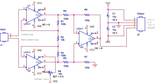
The second design is aninstrumentation amplifierbased on three op-amps, shown in figure11 on the next page. In practice it is unlikely that the circuit would be built using three sepa-rate packages with single op-amps as in this design. Complete instrumentation amplifiers are available in 8-pin packages. Even if these were unsuitable, a quad package that contains four op-amps could be used although these lack the pins for trimming the offset voltage.
This design cannot be saved in the demonstration version of PCB Editor, which is limited to 10 components. Try omitting the decoupling capacitors, R1and R3.
VCC VEE VEE VCC VEE VCC VEE VCC VEE Inverting Non-inverting +15 V 0 V -15 V Output Offset null U1 LF411 NC = 8 U1 LF411 NC = 8 + 3 -2 V+ 7 V-4 OUT 6 B1 1 B2 5 C1 10u 16 V C1 10u 16 V R1 100k R1 100k R2 10k R2 10k R3 100k R3 100k R4 100k R4 100k C2 10u 16 V C2 10u 16 V R5 100k R5 100k R6 100k R6 100k R7 100k R7 100k U3 LF411 NC = 8 U3 LF411 NC = 8 + 3 -2 V+ 7 V-4 OUT 6 B1 1 B2 5 J2 Output J2 Output 1 2 3 4 R8 10k SET = 0.5 R8 10k SET = 0.5 U2 LF411 NC = 8 U2 LF411 NC = 8 + 3 -2 V+ 7 V-4 OUT 6 B1 1 B2 5 J1 Input J1 Input 1 2
Figure 11. Instrumentation amplifier based on three op-amps. The labelNC = 8on the op-amps is not normally visible and will be explained later.
4.1
Schematic capture
Create a new directory for this design, as always, and start a new project in Capture. Place the components on the schematic but do not connect them yet. The only unfamiliar component should be the potentiometer, which is calledPOT– search for it.
Power supply rails are normally hidden to simplify schematic drawings. Here the power pins of the opamps are connected to namedpower symbols. Capture considers all power sym-bols with the same name to be connected together. Ground (earth) symsym-bols work in the same way. (Often the power pins themselves are hidden and connected purely by name.) Connect the power supplies as follows.
1. Select Place > Power. . . or click the power symbol button on the toolbar and select
VCC_CIRCLE from the CAPSYM library. Use the same symbol for both +15 V and
−15 V supplies. Place one near each power pin, mirror it vertically if necessary and connect it to the pin with a short wire.
2. Double-click the name of each power symbol in turn and change the name to VCCfor positive andVEE for negative supplies respectively. This is a standard usage (but there are many others). Check the orientation of the op-amps carefully! Some are mirrored vertically to make the circuit clearer and this reverses the power connections as well. 3. In the same way, selectPlace > Ground. . . or click the ground button. UseGNDfrom
CAPSYM for the ground (earth) symbols. These symbols must have the same name throughout your drawing or they will not be linked.
Table 2. Components and footprints for the instrumentation amplifier.
Part Capture name Footprint
Resistors R res400
Capacitor, electrolytic C_elect cap196 Connector, input HEADER 2 jumper2 Connector, output and power HEADER 4 jumper4
Op-amp LF411 dip8_3
Potentiometer (trimmer) POT pot
Two of the op-amps have unconnected pins. These pins are intentionally unused because they are for offset adjustment and it is only necessary to do this on one op-amp. PCB Editor must be told about this, otherwise it assumes that you omitted the connections by mistake and flags an error. Show that the pins are deliberately unconnected by choosing Place > No Connect from the menu bar or clicking the appropriate button, then clicking on the pins. A small cross appears as in figure11 on the preceding page. PCB Editor requires every pin to be connected or explicitly marked as not connected.
Next enter the footprints. Table 2shows suitable choices from the Cadence library for the new components.
Fixup. Incompatibilities between Capture and PCB Editor must again be corrected before making the netlist. First, the pins of the electrolytic capacitors are wrongly numbered. Repeat the instructions in section2.3 on page 8to fix this. ¦
Fixup. A new problem is that only 7 pins are defined on the electrical symbols for the op-amps but the package has 8 pins. You might hope that the software would assume that undefined pins are not connected but it does not: It must be told this formally.
1. Select one of the op-amps and chooseEdit > Part, which brings up the Part Editor. 2. ChooseOptions > Part Properties. . ., which brings up the list of User Properties. 3. Click theNew. . . button. Give the new property the nameNC, which stands for No
Con-nect, and the value8, which is the number of the unconnected pin. (Use a list separated by commas, such as7,8, if more pins are not connected.)
4. ClickOKto get rid of the dialog boxes and close the Part Editor. ChooseUpdate Allso that this change is applied to all LF411 parts in your design.
I have made theNCproperty visible on the schematic in figure11 on the previous page, which therefore showsNC = 8, but you would probably not do this in practice.¦
Run a Design Rules Check and correct any errors. Print your schematic when it has been completed and survived the DRC.
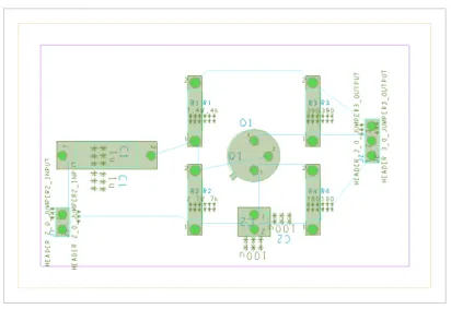
Figure 12. Quickplaced components for instrumentation amplifier just above board outline.
4.2
Create the PCB and place the components
Remember to make anallegrodirectory first. Set up the board as before (section2.5 on page 10) but make it 3.500×2.500, which gives you plenty of room for the larger number of components. Save the board and quit from PCB Editor. Back in Capture, create a netlist and send the design to PCB Editor as before. Check the Session Log: Ignore any warnings about RVMAX but investigate any others.
We’ll place the components using a different technique this time. Choose Place > Quick-place. . . from the menu bar. The defaults should be suitable (Place all components, Around package keepin, Top). ClickPlacethenOK. Your components are now arranged at the top of the board as shown in figure12, ready for you to move them into position. (OrCAD Layout did this automatically.)
Move the components onto the board, arrange them to resemble the schematic drawing and adjust them to make the ratsnest simple with as few crossings as possible (it is not possible to eliminate all of the crossings). This step is really important. It is easy to route the tracks on a well-placed board; conversely, a poorly-placed board needs long, convoluted tracks or may even be unroutable.
Run a Design Rules Check when the components have all been placed and save your board.
Note. Some students complain that Quickplace has not placed their components. The usual problem is that the screen has been zoomed to fit the board but the components are above the board and therefore out of sight!
Sometimes PCB Editor hides the ratsnests for the power and ground nets; it depends on how the nets were configured in Capture. See sectionC.5 on page 55to restore them. ¦
Figure 13. Constraint manager after changing the widths of the three power nets.
4.3
Add mounting holes
Most PCBs need to be mounted inside a piece of equipment and therefore need holes for fixings. Mounting holes and similar features are calledmechanical symbolsand are placed in a slightly different way from electronic components because they are not part of the netlist.
1. Select Place > Manually. . . to open the Placement dialogue box, bring the Advanced Settings tab forward and choose to Display definitions from Library. This is necessary because the symbols are not in the database imported from Capture.
2. Return to the Placement List tab and select Mechanical symbols from the drop-down list. 3. Use the same procedure as before to place a MTG156 symbol near each corner of the board. This is a hole of diameter 156 mils or 32500. Do not place the holes too close to the edge or the board may break when it is drilled.
Mounting holes are shown on my routed PCB in figure18 on page 34.
4.4
Preparation for routing
Power tracks are usually made wider than signal tracks because they have to carry more current. Our tracks are already so wide that it’s barely necessary but we’ll do it for future reference.
1. Choose Setup > Constraints > Physical. . . from the menu bar. This brings up the Constraint Manager and a Tip of the Day if you are unlucky (sigh).
2. The left-hand part of the window shows the various properties that can be edited. Click onAll LayersunderNet. See figure13for guidance.
3. The design part of the window now shows a list of the nets in your design. Most of them have random-looking numbers, such as N17311, but a few are named. These are the nets that carry power, to which we assigned names in Capture:VCC,VEEandGND_POWER
or something similar, depending on the symbol that you chose.
4. Change the minimum width for these three nets from 25 to 50 mil. These are in the column underLine WidthandMin. (I have changed other defaults in figure13but don’t worry about these for now; I’ll explain in sectionC.6 on page 56.)
5. ChooseFile > Closeto return to PCB Editor.
Save a copy of your board before routing so that you can use it for double-sided routing.
4.5
Autorouting a single-sided board
The instrumentation amplifier is simple enough that it is easy to route the tracks by hand and this gives the best layout. However, manual routing is impracticable for large boards and we shall therefore use the autorouter to gain experience of the procedure. You will do this twice: first as a single-sided board as in the one-transistor amplifier, and later as a double-sided board. It is possible to route all tracks on the single-sided board if you have laid it out well but the double-sided board should have a simpler layout with a smaller total length of track.
Two approaches are available for routing the board automatically, both shown in figure1 on page 4: Everything can be done from within PCB Editor or you can run the router as a separate application. The first is more convenient but the second offers finer control.
Autorouting may not be possible with the demonstration version of PCB Editor.
Autorouting from within PCB Editor
ChooseRoute > PCB Router > Route Automatic. . . from the menu bar. This brings up the Automatic Router dialogue box shown in figure 14 on the next page. Unfortunately it often causes a fatal error message that SPECCTRA quit unexpectedly with an exit code of 3, in which case you must use the other method.
Note. I have no idea what causes this; some computers in a classroom work while others fail, despite a nominally identical installation. ¦
SelectUse smart routerfor the Strategy. For a single-sided board deselect the box next to the TOP Routing Subclass. You might wish to experiment with the Routing Direction for the bottom layer. ClickRouteand wait for the results to come back. Use theResultsbutton to get a report on the routing and check the Completion percentage to ensure that all nets were routed successfully. Confirm this withDisplay > Status. . . and save your board.
If you can’t locate DRC errors, choose Tools > Quick Reports > Design Rules Check Reportfrom the menu bar. This gives a table of all errors including hyperlinks to their location. After all tracks have been successfully routed, choose Route > Gloss. . . from the menu bar. Glossingmeans to tidy up the design. This includes spreading tracks apart where possible and replacing 90° corners by 45° bends (mitering). Accept the defaults and gloss your design. Finally, useTools > Quick Reports > Etch Length by Layer Reportto find the lengths of the tracks and add them up. In general, a better design has shorter tracks.
Figure 14. Dialog box for running the autorouter from within PCB Editor.
Note. The gloss command occasionally appears to unroute some of the tracks, which revert to lines of ratsnest. UseView > Refreshto redraw the display and check carefully. Abandon the glossing if it has damaged your routing. ¦
Autorouting with OrCAD PCB Router
Use the manual equivalent of the flow described in the previous section if automatic routing does not work from PCB Editor. It’s a bit clumsier but gives better control over the process and makes it easier to experiment with different settings.
Note. At some point you may get aLicensing Errorwarning from PCB Router. ClickIgnore Feature for This Sessionif it appears. ¦
1. Choose File > Export > Router from the menu bar of PCB Editor. It asks you for a name for the Auto-Router Design file and you can probably accept the suggestion. Click
Run. You may be warned about overwriting the file, which isn’t a problem. A message
Translation Completedshould appear, after which you can close the box.
2. Start OrCAD PCB Router from the WindowsStart menu. You are presented with the fairly complicated dialogue box shown in figure 15 on the following page. Use the
Figure 15. Startup dialogue box for importing a design into PCB Router.
Figure 16. Screenshot of PCB Router with the instrumentation amplifier. I have changed the background of the window to white for a clearer printout. This design uses different footprints and the diagonally hatched areas show route keepouts, where tracks are forbidden.
Figure 17. Settings in the Layers box for single-sided routing on the bottom layer and double-sided routing on both layers.
• For theDesign / Session File(the first), choose the file that you just exported from PCB Editor.
• For theDo File(the last), choose the file with_rulesappended to the name of your board file.
ClickStart Allegro PCB Routerto dismiss the box. PCB Router starts and you should now see your components joined by the ratsnest within the outline of the route keepin as in figure16 on the previous page. Some components have shaded footprints, which I’ll explain later.
3. Tell PCB Router to route only the bottom layer. ChooseView > Layers. . . from the menu bar. Turn routing off for the top layer by clicking on the drop-down menu next to TOP
as shown in figure17and selecting thesymbol. You might like to experiment with the setting of the BOTTOM layer. The directions are hints to the router but in practice tracks are drawn in both directions. ClickClosewhen you have finished.
4. Choose Autoroute > Route. . .. Leave Smart selected and click OK. The autorouter works away and you will seeMessage: Smart_route finished, completion rate: 100.00%
if all is well. The tracks should be in colour if they are routed successfully, yellow for the bottom. Sometimes they are drawn white, which should indicate a design rules error, even when they are correct – I don’t know why.
See the suggestions below if the autorouter is unable to route your board.
5. Two further commands improve the tracks for assembly. First chooseAutoroute > Post Route > Spread Wires. . . and accept the defaults. This spreads the tracks away from each other and from the solder pads.
6. You’ll have noticed that the autorouted board has 90° bends in the tracks, which I told you to avoid when you routed the board by hand. We’ll now sort this out. RunAutoroute > Post Route > [Un]Miter Corners. . . and accept the defaults. Corners are rounded off and tracks run diagonally where possible.
7. To see the details of the finished layout, choose Report > Route Status. This may show a lot more than you want to know! Look near the bottom and confirm that the
Unconnected lengthis zero. TheRouted lengthis also given here.
8. Choose File > Quit. . . and agree to Save and Quit. This writes a session file that describes the routed tracks.
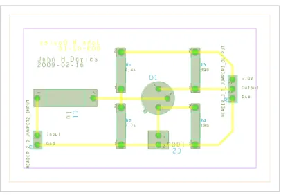
Figure 18. My one-sided layout after autorouting. The total routed length was 29.300. The footprints are not taken from the Cadence library.
9. Return to PCB Editor and choose File > Import > Router. . .. Locate the Session File
whose name matches your board and clickRun. You should see a messageTranslation Completed. Close the box.
10. The window now shows your design with tracks instead of the ratsnest. Save it under a different name to preserve the unrouted board for later.
Help! – My board won’t route
Here are some suggestions for helping the autorouter.
1. If routing has almost worked (only one or two unrouted segments), try changing the hints given to the router. For the one-sided board there is only the suggested direction of tracks. It is best to unroute the board and begin afresh. ChooseEdit > Delete Wires > All Wires
from the menu bar of PCB Router or reload the unrouted version of your board in PCB Editor.
2. If you are far from success, look at the layout to see where the problems lie. Often one particular track prevents successful routing. Can you rearrange the components to solve the problem?
Quit from PCB Routerwithout saving, or reload the previous version of your board in PCB Editor. Rearrange or reorientate components to make the ratsnest simpler and ease the problem before trying the autorouter again.