USING ORDERED PARTIAL DECISION DIAGRAMS
FOR MANUFACTURE TEST GENERATION
A Thesis by
BRADLEY DOUGLAS COBB
Submitted to the Office of Graduate Studies of Texas A&M University
in partial fulfillment of the requirements for the degree of MASTER OF SCIENCE
December 2003
Approved as to style and content by: M. Ray Mercer (Chair of Committee) A. L. Narasimha Reddy (Member) Michael Grimaila (Member) Chanan Singh (Head of Department)
USING ORDERED PARTIAL DECISION DIAGRAMS
FOR MANUFACTURE TEST GENERATION
A Thesis by
BRADLEY DOUGLAS COBB
Submitted to Texas A&M University in partial fulfillment of the requirements
for the degree of MASTER OF SCIENCE
December 2003
ABSTRACT
Using Ordered Partial Decision Diagrams for Manufacture Test Generation. (December 2003) Bradley Douglas Cobb, B.S., Texas A&M University
Chair of Advisory Committee: Dr. M. Ray Mercer
Because of limited tester time and memory, a primary goal of digital circuit manufacture test generation is to create compact test sets. Test generation programs that use Ordered Binary Decision Diagrams (OBDDs) as their primary functional representation excel at this task. Unfortunately, the use of OBDDs limits the application of these test generation programs to small circuits. This is because the size of the OBDD used to represent a function can be exponential in the number of the function's switching variables. Working with these functions can cause OBDD-based programs to exceed acceptable time and memory limits. This research proposes using Ordered Partial Decision Diagrams (OPDDs) instead as the primary functional representation for test generation systems. By limiting the number of vertices allowed in a single OPDD, complex functions can be partially represented in order to save time and memory. An OPDD-based test generation system is developed and techniques which improve its performance are evaluated on a small benchmark circuit. The new system is then demonstrated on larger and more complex circuits than its OBDD-based counterpart allows.
ACKNOWLEDGMENTS
I would like to thank my advisor Dr. M. Ray Mercer for all of the invaluable knowledge, support, advice, and opportunities that he has given me.
I would also like to thank the other members of my committee, Dr. A. L. N. Reddy and Dr. M. R. Grimaila, for being excellent teachers and supportive mentors.
I would like to thank my parents for their love and support throughout my entire life and for always encouraging me to “do your best and be your best.”
I would like to thank my wife Christina for always being there for me and reminding me of the most important things in life.
I would like to thank Jennifer Dworak, Jimmy Wingfield, and Dr. Sooryong Lee for teaching me by example how to be a successful student and researcher and for listening to my ideas and problems.
I would like to thank Carolyn Warzon and Tammy Carda for their guidance and their effort in helping me to meet all of the university’s administrative requirements.
I would like to thank the Department of Electrical Engineering at Texas A&M University for providing me with excellent educational opportunities and financial support.
Finally, I would like to thank God for the many blessings and opportunities that He has provided me with, and for giving me the strength to persevere through difficult times.
TABLE OF CONTENTS
Page
ABSTRACT ... iii
ACKNOWLEDGMENTS...v
TABLE OF CONTENTS ...vi
LIST OF FIGURES...vii
LIST OF TABLES ... viii
INTRODUCTION...1
Testing for Manufacture Defects...1
Stuck-at Fault Testing ...3
Exciting, Observing, and Detecting a Fault ...4
Multi-Detect Testing ...5
Fault Excitation, Observation, and Detection Probabilities ...6
Binary Decision Diagrams ...6
An OBDD Package for Manufacture-Test Generation ...8
Limitations of OBDD Test Generation Packages ...10
Ordered Partial Decision Diagrams...10
OPDD-Based Test Generation ...11
METHOD...13
Converting OBDD Graphs to OPDD Graphs...13
Removing Multiple Vertices from a BDD ...16
Calculating Observation Functions using D-Propagation ...17
Enhancements to D-Propagation ...23
Excitation Guidance ...25
Terminal Vertex Combination...28
Other Speed Improvements to sByDDer...30
Test Generation ...30
RESULTS...32
Overview ...32
Method Evaluation ...33
Test Generation for Larger Circuits ...41
CONCLUSIONS ...47
REFERENCES...49
LIST OF FIGURES
Page
Figure 1. Integrated circuit production flow ...1
Figure 2. AND network...3
Figure 3. AND gate with output stuck-at-zero ...4
Figure 4. Exciting, observing, and detecting a fault...5
Figure 5. Example OBDD ...7
Figure 6. Example OPDD ...11
Figure 7. Input combination values for example OBDD ...14
Figure 8. Vertex removal metric calculation...16
Figure 9. Boolean-difference observation function calculation ...18
Figure 10. Boolean-difference unguided...20
Figure 11. Boolean-difference partially guided ...21
Figure 12. Boolean-difference fully guided ...22
Figure 13. D-propagation through multi-input gates ...24
Figure 14. Excitation guidance procedure...27
LIST OF TABLES
Page
Table 1. Method abbreviations...33
Table 2. Unknown excitation OPDDs of non-redundant faults ...34
Table 3. Unknown observation OPDDs of non-redundant faults ...34
Table 4. Unknown detection OPDDs of non-redundant faults ...35
Table 5. Percentage of excitation minterms known ...36
Table 6. Percentage of observation minterms known ...36
Table 7. Percentage of detection minterms known ...36
Table 8. Single-excitation guidance vs. dual-excitation guidance - D-TVC...37
Table 9. Size of single-detect stuck-at-fault test set (vectors)...38
Table 10. Faults undetected by fault simulation ...38
Table 11. Multi-input Apply ordering - D-TVC-DEG...39
Table 12. BDD-Crusher time (seconds) - D...39
Table 13. Runtime (minutes)...40
Table 14. Removing multiple vertices (Unknown detection OPDDs) - D-TVC-DEG....40
Table 15. Variations on the RMV option - D-TVC-DEG-256 ...41
Table 16. c880 - D-TVC-DEG ...43
Table 17. c3540 - D-TVC-DEG ...44
INTRODUCTION
Testing for Manufacture Defects
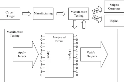
The production of integrated circuits (IC) has exploded into a multi-billion dollar industry whose customers consistently demand faster and more intelligent products. In response to these demands, companies manufacture ICs that are growing increasingly larger and more complex. As with any mass produced product, a strong quality control system must be in place to assure that very few, if any, defective parts are sold. This is because the cost, both in terms of profit and reputation, of repair and replacement of shipped defective parts far exceeds the cost screening out the defective parts in the first place. For integrated circuits, this quality control is enforced by automatic test equipment as described by Turino in [1]. After the IC is manufactured, it is tested by the ATE to determine whether it is free from defects. Figure 1 shows where manufacture testing fits into the production flow of an IC.
Manufacturing Manufacture Testing Reject Circuit Design Apply Inputs Verify Outputs 1 0 1 0 1 0 1 0 1 0 1 0 1 0 0 0 1 1 1 0 0 0 1 0 Integrated Circuit In p u ts Ou tp u ts Ship to Customer Pass Fail Manufacture Testing
Figure 1. Integrated circuit production flow
To test an IC, the ATE enters multiple combinations of values into the circuit's inputs and observes the outputs to make sure they are correct. This is one of the only possible methods of testing because the ATE does not have access to any of the interior points in the circuit. Therefore, the goal of testing is to strategically choose the inputs to the circuit so as to cause any interior defects in the circuit to manifest themselves as erroneous logic values at the circuit's outputs.
One possible strategy to test for a combinational circuit's defects is to apply every possible input combination to the circuit and verify that the output values it produces are correct. This strategy will completely test the circuit’s static operation and was commonly applied to small circuits in the past. Unfortunately, today's large and complex ICs cannot be tested so easily. Applying every possible input combination requires2 different combinations to be applied, where n is the number of inputs and n storage elements in the circuit. Attempting to test a modern processor in this way using the fastest ATE available today would take at least thousands of years. Functional testing, in which test cases that exercise each of the circuit’s basic functions, is another popular testing alternative. Although this approach verifies basic functional correctness, it does not attempt to exercise all of the circuit’s structural elements. Clearly, a testing method that test’s all of a circuit’s structurally elements and requires entering far fewer than all of the possible input combinations must be used.
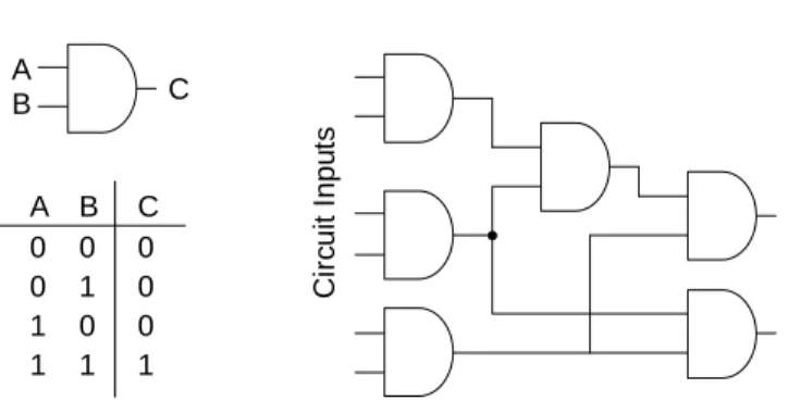
To fully understand the process of testing, one must have a basic knowledge of the basic components of an integrated circuit and how they operate. An integrated circuit can be considered a collection of interconnected building blocks called logic gates. The inputs to these gates can only take on the values of logic zero and logic one and can ideally only produce an output of logic zero or logic one. The specific function implemented by the integrated circuit is determined by how the gates are interconnected. A graphical representation of one specific gate, the AND gate, is shown in Figure 2 along with its outputs in response to all of the possible input combinations. Also in Figure 2 is an example network composed entirely of AND gates. Sixty-four input
combinations would need to be applied to the sample AND network to completely test all of the static defects.
C ir c ui t I npu ts C irc u it Ou tp u ts A B C A B C 0 0 1 1 0 1 0 1 0 0 0 1
Figure 2. AND network
Stuck-at Fault Testing
Determining which of the input combinations, or test vectors, to use when testing an IC depends on the chosen testing strategy. The most common approach used in industry today is based on the single stuck-at fault model developed by R. D. Eldred in [2]. A fault model is a simplified specification of a likely defect in an IC. The single stuck-at fault model, often simply referred to as the stuck-at fault model, assumes that the only defects that can occur are points in the circuit that are erroneously fixed to a logic zero (stuck-at zero) or a logic one (stuck-at one). This can occur when two parts of a circuit are either erroneously connected together or not properly connected at all. For example, such a defect can force a point in the circuit to be either grounded or pulled to a high voltage regardless of what the circuit's inputs dictate it to be. Figure 3 shows an AND gate with a static defect that generates an erroneous output of logic zero when both inputs are at logic one. As you can see, the output C does not assume the correct logic value when A equals logic one and B equals logic one. The single stuck-at fault model also assumes that only one fault will be present in the IC at a time. This simplifies the
model so that it does not have to deal with all of the possible multi-fault combinations that could be present in the IC. A typical testing strategy would involve generating a set of input vectors that tests for both types of stuck-at faults for every wire in a circuit.
A B C A B C 0 0 1 1 0 1 0 1 0 0 0 0 Stuck-at zero error
Figure 3. AND gate with output stuck-at-zero
Exciting, Observing, and Detecting a Fault
For a test vector to be successful at detecting a fault, it must accomplish both the tasks of exciting and observing the fault. Exciting a fault involves setting the inputs of the circuit to values that will cause a fault to produce erroneous values at its location, or site, in the circuit. In the case of exciting stuck-at faults, this is a simple as configuring the circuit to place a logic one (for stuck-at-zero faults) or a logic zero (for stuck-at-one faults) at the desired site. For example, to excite a stuck-at-zero fault at the output of a gate in a circuit, a test vector must be generated that will produce a logic one at the output of that gate in the non-faulty circuit, also known as the good circuit. When that test vector is applied to a faulty circuit with a stuck-at-zero fault at that same site, an erroneous logic value of logic zero will appear at that site instead of the correct value of logic one.
Observing a fault requires selecting the input vector so that it propagates the value at the desired fault’s site to at least one of the outputs of the circuit. Extending the above example, the chosen input vector must also be generated so that it propagates the value at the selected site to the circuit outputs. This propagation is accomplished by determining the connectivity paths from the fault site to the circuit outputs and setting
the side inputs to gates along these paths to non-controlling values. For example, if one of the paths passes through an AND gate, the circuit must be configured to place a logic zero at each of the other inputs to that gate. This will allow values to propagate through the AND gate along the desired path.
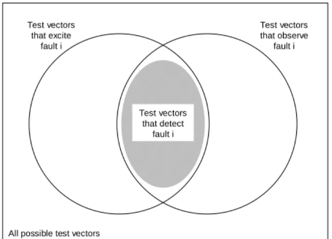
Test vectors that detect a fault must be able to both excite and observe the fault at the same time. This set of vectors can be thought of as the intersection between the set of vectors that excite the fault and the set of vectors that observe the fault, as demonstrated in the Venn diagram of Figure 4. The number of possible input combinations that will detect a fault depends on the size of the excitation and observation sets and on the overlap between them.
All possible test vectors Test vectors that excite fault i Test vectors that detect fault i Test vectors that observe fault i
Figure 4. Exciting, observing, and detecting a fault
Multi-Detect Testing
Testing strategies that require 100% detection of all the stuck-at faults in a circuit are successful because they require the generation of a test vector set that has the capability of making each site in the circuit observable at the circuit outputs. The weakness of the stuck-at fault model lies in the fact that its excitation requirements often do not match those of real circuit defects. To overcome this limitation, Grimaila [3]
demonstrated that applying test sets that detect each fault in a circuit multiple times, each with a unique input vector, detects more real manufacturing defects than the application of single-detect test sets. By applying multiple tests for a stuck-at fault, the fault can be excited in a different way each time. This increases the probability of matching the excitation criteria for a real defect that might be present at that site. Recently, multi-detect testing strategies are gaining favor in the testing community because they do not require complicated fault modeling but still achieve impressive results.
Fault Excitation, Observation, and Detection Probabilities
The probability that a fault will be excited, given that a random input vector is chosen, can be determined by dividing the number of vectors that excite the fault by the total number of vectors that can be applied to the circuit. The same technique can be used to find both the probability of observing and detecting a fault. These probabilities have been used in [4] to explore the relationships between the difficulty of exciting, observing, and detecting faults within a circuit. They were also used in [4] to explain and predict the difference in test set lengths between tests that target different fault models.
Binary Decision Diagrams
Binary Decision Diagrams (BDDs) were first proposed by Lee in [5] as a way to represent Boolean functions in the form of directed acyclic graphs. The BDD representation was later developed by Bryant in [6] into a more useful, canonical data structure called a Reduced Ordered Binary Decision Diagram (ROBDD), often simply referred to as an OBDD, which lends itself to more efficient manipulation by computers.
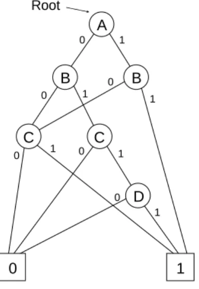
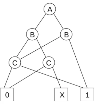
Figure 5 shows the OBDD for a simple logic function containing the switching variables A through D. The OBDD is composed of two types of vertices: switching-variable vertices and terminal vertices. The vertices at the very bottom of the graph are the square-shaped terminal vertices, and there exists one terminal vertex for each logic value that the function represented by the OBDD can produce. The circular-shaped switching-variable vertices in the graph are assigned to one of the function’s inputs.
Each switching-variable vertex has a logic-one arc and logic-zero arc leading away from it. These arcs connect the vertices to form a graph and are used to trace through the OBDD when evaluating an input combination. The vertex pointed to by an arc is called the child of vertex where the arc originated. For example, the logic zero terminal vertex is the zero child of the D vertex, and the logic one terminal vertex is the one child of the D vertex. The vertex at the top of the graph is called the root vertex, and the evaluation of all input combinations must begin here.
A B B C C D 1 0 0 0 0 0 0 0 1 1 1 1 1 1 Root
Figure 5. Example OBDD
To evaluate the function in Figure 5 when A equals one, and B equals one, C equals zero, and D equals one, first start at the root vertex and proceed down the graph by following the appropriate arcs. In our example, the root vertex is assigned to the variable A, and because we want to evaluate the functions when A equals one, we follow the arc labeled with a one away from the root vertex. This leads to the vertex assigned to the variable B. At the B vertex we follow the arc labeled with a one, corresponding to B equals one, to the terminal vertex logic one. Thus we have found that the function A AND B evaluates to logic one when both A and B equal one. Often a standard
convention is used in place of the labels on the arcs. In these cases, the arcs that point left are the zero arcs, and the arcs that point right are the one arcs.
All of the normal Boolean operations such as AND, OR, NOT, and XOR can be performed quite easily on OBDDs. Boolean operations between two OBDDs are carried out using an algorithm called the Apply operation, which was efficiently implemented by Bryant in [6]. The Apply operation produces an OBDD with the correct function, but often with redundancies in its structure. Therefore, a Reduce operation is called on the resulting OBDD to eliminate the redundancies. This is generally required to convert the OBDD into its canonical form.
One important feature of OBDDs is the fact that their vertices follow a strict order. This means that when tracing through the graph of an OBDD, the Boolean variables will always be encountered in the same order. This is another requirement that makes OBDDs a canonical form. In addition, choosing the correct variable ordering for an OBDD can, for some functions, greatly affect the number of vertices required to represent it.
Because OBDDs are a canonical form for representing Boolean functions, they lend themselves to easily performing common tasks such as finding input combinations that satisfy a function, testing functions for equivalence, and combing functions with a Boolean operation. Given these and other advantages, OBDDs have found wide application to such CAD problems as logic synthesis [7], logic verification [8], and manufacture-test generation [9].
An OBDD Package for Manufacture-Test Generation
In [9], a test generation package named sByDDer was developed. sByDDer uses OBDDs as its primary data structure and the Apply operation as its primary manipulation tool. To generate tests for stuck-at faults in a combinational circuit, sByDDer passes through four major phases. The first phase involves calculating the sets of all tests that excite each fault in the circuit. This is done in a single forward pass through the circuit, by first creating the primary input OBDDs then calling the Apply operation to calculate the output of each gate. sByDDer then proceeds to find the sets of
all tests that observe each fault. This is done by using a method that calculates the Boolean-difference of each fault site with respect to the primary outputs. In the third phase, sByDDer then determines the set of all tests that detect each fault by finding the intersection of the excitation and observation sets for that fault. The intersection is accomplished by computing the AND of the excitation and observation OBDDs using the Apply operation. Finally, sByDDer selects a subset of the generated tests to be included in the final test set. The final test set can be either a single-detect or multi-detect test set.
Functionally-based OBDD test generation packages such as sByDDer are useful for many reasons. Recent work by Dworak [4] utilized sByDDer’s facilities to produce the exact fault excitation, observation, and detection probabilities of various benchmark circuits. This information was used to explain and predict the difference in test-set lengths between test sets that target stuck-at faults verses transition faults. S. Lee used the sByDDer package in [10] to generate truly random manufacture tests for each fault in a circuit. These random test sets were then used as an approximation of current industry practice in test generation and served as benchmarks for evaluating the effectiveness of newly proposed test generation strategies.
OBDD-based test generation packages also excel in creating compact test sets and multi-detect test sets. Traditional, structurally-based test generators produce only one test at a time and must be run iteratively to obtain multiple tests for each fault. Because OBDD-based test generators work on the functional level, they automatically produce all possible tests for each fault. Having a large set of candidate tests for each fault is a great benefit for test-set compaction techniques, allowing them to more easily find the smallest number of tests that will detect all of the faults in a circuit. This advantage was explored by Wingfield in [9] where sByDDer was used to successfully generate compact test sets near the theoretical minimum length presented in [11]. The functional representation used by OBDD-based test generators also lends itself to the creation of multi-detect test sets. In [9], the author showed that the multi-detect test sets
generated by sByDDer were vastly smaller in size than those generated by a more traditional tool.
Limitations of OBDD Test Generation Packages
Although OBDDs provide many benefits in the area of CAD and manufacture testing, their use can be costly in terms of both memory and computational time. Because the memory requirements of OBDDs can be determined by the variable ordering chosen to represent them with, much research has been done in the area of optimal variable order selection. Unfortunately, it has been shown in [6] that regardless of the chosen variable ordering, some functions exist which require an exponential amount of memory resources when represented as OBDDs. Because of these limitations, most of the work done using OBDDs, as in [4] and [9], has been limited to the smallest benchmark circuits that have OBDDs of tractable size. When larger circuits are attempted by a package such as sByDDer, one of two things occurs. Either the required memory exceeds the available RAM on the machine, resulting in memory thrashing, or the large OBDDs cause the Apply operations to take an excessive amount of time to complete. Under both circumstances, the test generation process cannot be completed within a practical time limit.
Ordered Partial Decision Diagrams
In order to overcome the limitation of OBDD-based applications, a solution was needed to make OBDDs more widely applicable to larger, more complex functions. Towards this end, a variation on the OBDD called an Ordered Partial Decision Diagram (OPDD) was introduced in [12]. OPDDs contain a subset of the functional information contained in OBDDs, but at a lower cost in terms of memory and manipulation time. Figure 6 shows an example of a partially specified function represented as an OPDD. It represents the same function as the OBDD in Figure 5, but with only partial information. As you can see, a third terminal vertex named X has been introduced into the structure in place of one of the vertices containing the variable C. Now when evaluating the function for a specific input combination, the evaluation path taken through the OPDD
has the possibility of ending at the X terminal instead of the logic zero or logic one terminal. For these input combinations, the value of the function is unknown. Converting an OBDD to an OPDD by replacing some of its vertices with the X terminal generally reduces the total number of vertices in the graph, but at the loss of functional knowledge. Therefore, a primary goal when working with OPDDs is to find the optimal tradeoff between graph size and functional knowledge.
A B B C C 1 0 X
Figure 6. Example OPDD
One of the first and most widespread applications of OPDDs, researched by [13], [14], and [15], was in the area of determining the optimal variable ordering for OBDDs. OPDDs have also been used for logic verification [16] and OBDD partitioning [17]. In these and other applications, OPDDs have allowed many of the techniques developed using OBDDs to be extended to circuits of much greater size and complexity than ever before achieved.
OPDD-Based Test Generation
Based on the results mentioned above, an OPDD test generation package has been created. Building on the sByDDer engine by incorporating OPDDs into the package, it is able to handle larger and more functionally complex circuits. Using OPDDs as the primary data structure reduces the memory and time requirements that
previously limited sByDDer’s application to larger circuits. This has been accomplished by limiting the maximum size of a BDD produced as the result of an Apply operation. Of course, not all of the advantages of an OBDD test generation package can be retained with the introduction of OPDDs. Although OPDDs require less memory and time to process, by definition they do not contain as much functional information as their OBDD counterparts. Therefore, a large effort is required to maximize the useful information content of the OPDDs used to represent fault excitation, observation and detection functions. For the same reason, the test selection process will be less optimal when working with OPDD, limiting the possibilities of test compaction techniques.
METHOD
Converting OBDD Graphs to OPDD Graphs
When an Apply operation is performed on two BDDs, the resulting BDD will often contain more vertices than either of the original BDDs. In fact, this is one of the only operations used in sByDDer that creates larger BDDs than previously exist. Because the goal of this research is to limit the size of the BDDs operated on during sByDDer’s test generation process, in turn reducing the memory and time requirements of the application, a limit is placed on the size of the resulting BDD from an Apply operation. This limit is enforced by eliminating vertices from the BDD until it reaches the predefined user specified limit. For example, if the maximum number of vertices is limited to fifty vertices and the Apply operation produces a BDD with fifty-five vertices, at least five vertices are removed from the BDD before sByDDer is allowed to continue.
A vertex is removed from a BDD by replacing it with the X terminal. The represented function is then unknown for the input combinations who’s paths originally passed through the removed vertex. Therefore, the goal when removing vertices is to retain the most information possible about the function represented by the BDD. Take for example the situation where only one vertex must be removed from the BDD in order for it to satisfy the limit on the maximum number of vertices. Also, assume that the BDD is an OBDD and therefore does not contain an X terminal. One option for determining which vertex to remove would be to try removing each vertex in the BDD one at a time and observe how many entries in the truth table of the resulting function evaluate to X. The vertex that affects the fewest truth table entries can then be removed.
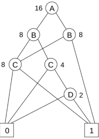
A more practical way of approaching the problem is to pass information down the BDD, starting at the root vertex, about the number of input combinations that pass through each vertex. For example, all input combinations pass through the root vertex at the top of the BDD. Therefore, a value of 2n, where n is the number of variables in the function, is associated with the root vertex. Moving down the BDD, half of the input combinations flow through each of the two arcs leaving the root vertex and pass through
the vertices at the second level of the graph. A value of 2n/2 will then be associated with those two vertices on the second level. This pattern continues as each vertex passes half of its value down each of its two arcs to the vertex below it. After these values have trickled down the BDD, each vertex has a value associated with it that corresponds to the number of truth-table entries which will become unknown if the vertex is removed. The optimal vertex to remove is the therefore the vertex with the smallest value associated with it. Figure 7 shows what the actual values would be for our example function. As you can see, the vertex representing the variable D has the smallest value. Therefore, the removal of vertex D would cause the smallest reduction in functional knowledge.
A B B C C D 1 0 16 8 8 8 4 2
Figure 7. Input combination values for example OBDD
The previous version of sByDDer has the functionally to calculate the input combination values mentioned above, but in an inefficient way. It passes these values down the BDD in a depth-first manner using a recursive algorithm. For example, at the root vertex, the value is first passed down to it zero child, and then the zero child proceeds to pass a value to its zero child. This pattern continues until a terminal vertex is reached. At that point, the algorithm backtracks up to the previous vertex and passes a
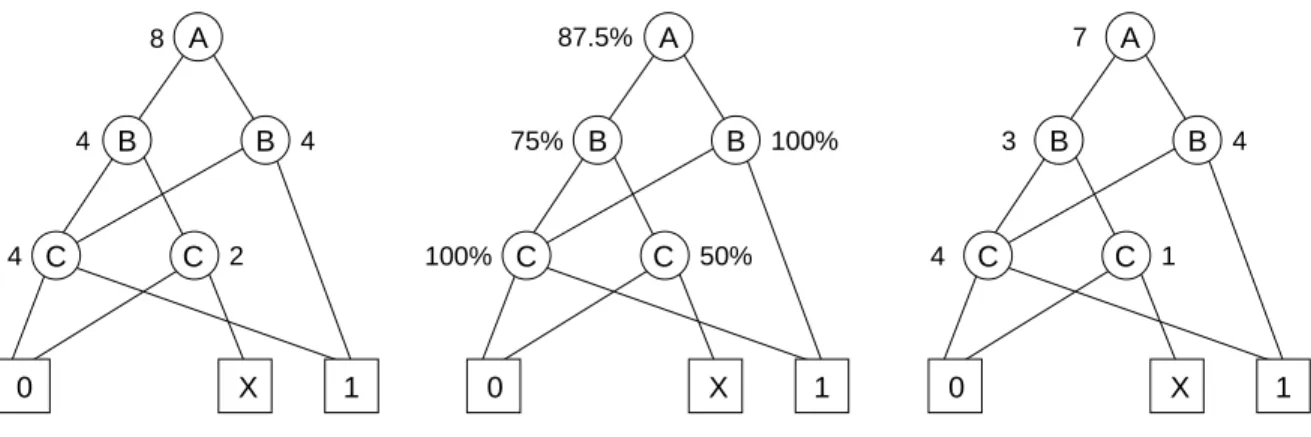
value down to its one child. The drawback to this algorithm is that it has the possibility of visiting a single vertex in the BDD many times. Vertices that have multiple arcs pointing to them will be visited one time for each arc. The new version of sByDDer contains a modified algorithm that passes the values down the BDD in a breadth-first manner. A vertex is only processed when all of the vertices upstream from it have been processed. This guarantees that each vertex in the BDD will only be visited once. Therefore, the breadth-first algorithm always requires linear time with respect to vertex count as opposed to the possibly exponential time requirements of the depth-first algorithm. In our example function, the far left vertex containing the variable C would be visited only once by the breadth first algorithm, but twice by the depth first algorithm. The vertex removal procedure previously described requires a modification if the oversized BDD already contains an X terminal. In short, the vertex whose removal will convert the fewest additional truth-table entries to unknown should be chosen. This information can be obtained by making an additional pass through the BDD, starting at the terminal vertices and passing information up the graph. The information that should be passed up the graph is the percentage of input combinations that pass through the vertex and end at the known vertices of zero or one. These percentage-known values can be efficiently calculated as follows. Starting with the terminal vertices, a value of zero percent is associated with the X terminal and a value of 100 percent is associated with the zero and one terminals. Next, the percentage-known values associated with the parents of the terminal vertices are calculated. The percentage-known value for a vertex is obtained by simply summing its children’s percentage values and dividing by two. Once all of the percentage-known values have been calculated, the percentage-known value for each vertex should be multiplied by the number of input combinations that pass through that vertex. The resulting value is called the removal metric. As before, the vertex with the smallest value for this metric should be removed. Figure 8 shows an example of how these metrics are computed. The leftmost OPDD show the number of input combinations that pass through each vertex. The center OPDD shows the percentage-known values for each vertex, and the rightmost OPDD shows the removal
metric for each vertex. The metrics indicate that the rightmost C vertex is the optimal choice for removal.
A B B C C 1 0 X 8 4 4 2 4 A B B C C 1 0 X 87.5% 75% 100% 50% 100% A B B C C 1 0 X 7 3 4 1 4
Input Combination Values Percentage Known Values Vertex Removal Metrics
Figure 8. Vertex removal metric calculation
As a final step after the removal of a vertex, the Reduce operation should be called on the resulting OPDD to eliminate any redundancies introduced by the conversion of that vertex to an X terminal. This can further reduce the number of vertices in the OPDD without losing any functional information. For example, converting a vertex to an X terminal might result in two identical sub-trees inside the BDD, one of which can be removed for a substantial savings. The arcs previously pointing to the root of the removed sub-tree are then redirected to the root of the retained sub-tree.
Removing Multiple Vertices from a BDD
So far we have only considered the case where only one vertex must be removed to bring the BDD down to an acceptable size. The vertex removal process is not as straightforward for the cases where multiple vertices must be removed. Converting only one vertex to an X terminal and calling the Reduce operation as described above will sometimes remove a sufficient number of vertices. This will generally work when the number of excess vertices is small, but the probability that calling the Reduce operation
will be sufficient diminishes as the number of excess vertices increases. One simple solution to this problem is to repeat the steps of converting a vertex to an X terminal and calling the Reduce operation iteratively until the OPDD reaches an acceptable number of vertices. While not optimal, this method avoids considering the effects that all possible combinations for removing multiple vertices at one time will have on the number of known truth-table entries. It also avoids having to consider which combinations of vertices will result in the greatest reductions when the Reduce operation is called.
One of the major negative aspects of the iterative single-vertex removal algorithm is its time requirements. As an example, consider an Apply operation between two BDDs with 500 vertices each. In the worst case, the resulting BDD can be 250,000 vertices. All but 500 of these vertices must be removed, which means that the iterative removal algorithm could have to be called 249,500 times for one Apply operation. For each iteration the removal metrics must be recalculated, the desired vertex must be found and removed, and the Reduce operation called. The repetition of these steps can require a considerable amount of time.
One solution to speed up the algorithm involves calculating the removal metrics only once, removing all of the excess vertices at once, and calling the Reduce operation only once at the end. Although this method is less optimal, the time saved when dealing with large BDDs justifies its use in many cases. As a compromise between speed and quality, another variation can be used which involves determining the number of vertices to be removed based on the number of vertices still in excess of the vertex limit. For example, one-half of the excess vertices might be removed, Reduce called, and the removal procedure then called again to remove one-half of the remaining excess vertices. This loop can be iterated until the number of vertices has been reduced to the maximum limit.
Calculating Observation Functions using D-Propagation
The observation function for a site describes all of the possible input combinations that will make the logic value at that site visible at one or more of the circuit outputs. Calculating the observation functions for a circuit site is more
complicated than simply calculating the function itself at a site. sByDDer calculates the observation functions via a direct application of the Boolean difference. Figure 9 illustrates this process.
The Boolean difference of each output with respect the site-under-test if calculated, and the union of all the results is produced as the observation function. To calculate the Boolean difference for a site, two passes through the circuit are required, starting from the site-under-test and ending at the outputs. First, the function logic zero is inserted at the site-under-test and is propagated to the outputs, performing the Apply operation at each gate along the way. These are called the f0 residues for the site.
Second, the function logic one is inserted at the same site and propagated to the outputs in the same fashion. These functions are called the f1 residues for the site. An XOR
operation is then performed between the f0 and f1 residues at each output to create the
Boolean difference functions. Finally, the union of the Boolean difference functions is created by performing an OR operation between them.
2 0 f 1 0 f f11 2 1 f Obs f C irc uit I npu ts Site-Under-Test
Figure 9. Boolean-difference observation function calculation
There are two major drawbacks to calculating the observation functions in the manner described above, especially when working with OPDDs. The first drawback is the number and kind of operations required by the algorithm. Calculating each observation function requires visiting each gate between the site-under-test and the
outputs two times, resulting in twice as many calls to the Apply operation. In addition, the XOR operations performed at the end of the algorithm can be quite time consuming. The f0 and f1 residues at each output are most likely represented by OPDDs of the
maximum allowable size. Therefore, the Apply operation will probably take a large time to complete and the number of vertices to remove afterwards will be quite large.
The second major drawback centers on the separate calculation of the f0 and f1
residue functions. Because and XOR operations will be performed on these functions, any input combinations that are unknown for one of the residues will also be unknown in the resulting function. If the parts of the truth table that are known for each residue have very little overlap, then the observation function calculated from them will contain little functional information. On the other hand, if the known parts of the truth table greatly overlap, the observation function will contain more functional information. Unfortunately, the parts of the truth table that are known for each residue depend on the way vertices were removed by the all of the Apply operations that occurred along the propagation paths through the circuit. Additionally, only the minterms of the resulting function are input combinations that observe the site. The input combinations in the f0
and f1 residues must evaluate to opposite logic values to create a minterm in the function
computed by the following XOR operation. Therefore, even if the known parts of the truth table greatly overlap between the f0 and f1 residue functions, little useful
information about the resulting observation OPDD could be generated.
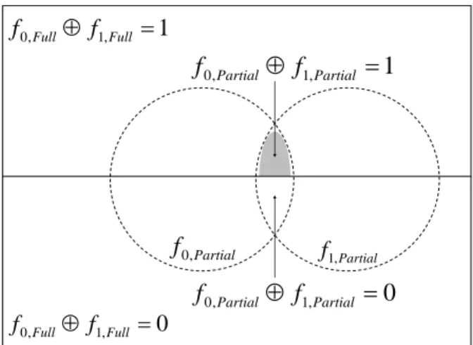
Consider the Venn diagram in Figure 10. The region inside the largest rectangle represents all of the possible input combinations to the circuit. The large region is divided horizontally to separate the input combinations into two sets. The top region contains the input combinations that observe the site at one of the circuit outputs, and the bottom region contains those input combinations that do not. After the first pass of the observation calculation algorithm, only a subset of the f0 function will be represented by
the resulting OPDD. This region is represented by the dashed circle labeled f0, Partial.
After the second pass, a subset of the f1 function will be represented by the resulting
of f0, Partial and f1, Partial is the maximum size of the region that can be represented by the
OPDD that results from the following XOR operation. The part of this intersection lies in the upper rectangle is the set of known input combinations that will observe the site. The part in the lower rectangle is the set of input combinations that will be known not to observe the site. In order to maximize the number minterms in the final observation BDD, two tasks need to be accomplished. The f0 and f1 OPDDs must be known for the
same input combinations and must evaluate to different logical values for as many of these input combinations as possible.
Partial f0, f1,Partial 0 , 1 , 0Full⊕ f Full = f 1 , 1 , 0Full⊕ f Full = f 1 , 1 , 0Partial⊕ f Partial = f 0 , 1 , 0Partial⊕ f Partial = f
Figure 10. Boolean-difference unguided
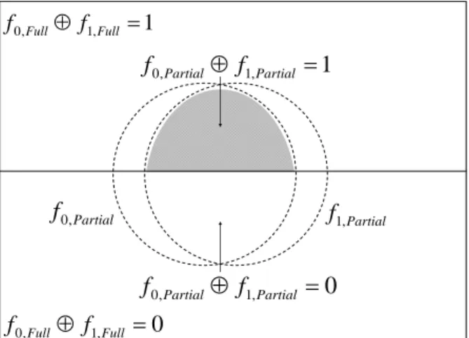
One possible solution is to use the functional information known from one pass to guide the removal of vertices during the second pass. For example, Figure 11 shows one possibility of what might happen if the choice of vertices removed in the f1 residue
was guided by the f0 residue to preserve input combinations in f1 that are known in the f0
residue. As shown in the figure, more input combinations will be included in the intersection set as a result of this technique. Therefore, this kind of guidance would most probably increase the amount of known functional information represented by the observation functions. But as you can see from the figure, one major drawback still
remains. Although the f0, Partial and f1, Partial greatly overlap, many of the overlapping
input combinations do not evaluate to different logical values in the residue functions. The vertices in the residue OPDDs that represent the input combination in the lower rectangle of the figure would have better been used to describe more of each residue function that lies in the upper rectangle. Ideally, both the creation of the f0 and f1
residues should be guided into the upper rectangle region as shown in Figure 12. This would be quite difficult to do without a priori knowledge about the complete residue functions. 0 , 1 , 0Full⊕ f Full = f 1 , 1 , 0Full⊕ f Full = f Partial f0, f1,Partial 1 , 1 , 0Partial⊕ f Partial = f 0 , 1 , 0Partial⊕ f Partial = f
Partial f0, Partial f1, 0 , 1 , 0Full⊕ f Full = f 1 , 1 , 0Full⊕ f Full= f 1 , 1 , 0Partial ⊕ f Partial = f 0 , 1 , 0Partial⊕ f Partial = f
Figure 12. Boolean-difference fully guided
As an alternative to calculating the observation functions by direct application of the Boolean-difference equation, a method called Propagation can be used. D-Propagation is a technique which inserts a new Boolean variable, D, at the site-under-test and attempts to propagate that D to the outputs by setting the side inputs of the gates along the propagation path to non-controlling values. The logic value D acts much like any other logic variable. When the logic value D is the input to an inverter, the logic value DBAR is produced at the output. As another example, when a logic value of D is on one of the inputs to an AND gate, the other inputs must have a value of logic one or D for a D to be produced at the output. An input pattern that successfully propagates a D to one or more of the outputs is therefore a minterm of the observation function for the site at which the D was inserted.
To calculate the observation function at a site, a BDD that consists of a singe D terminal is inserted at that site and propagated to the outputs. By simply calling the Apply operation again at each gate along the propagation path, all possible input combinations that observe that site can be found. If a vertex limit is imposed, some subset of entire set of possible input combinations can be found. Once the D value has been propagated to the outputs, the resulting BDDs are converted into traditional
observation BDDs. All of the D and DBAR terminals are changed to logic one terminals, and all of the logic one terminals are changed to logic zero terminals. Finally, an OR operation is performed among all of the BDDs at the outputs.
The D-propagation method of observation function calculation overcomes the aforementioned drawbacks to the direct Boolean-difference method. Only one pass is required through the circuit, which cuts the number of Apply operations in half. Also, there is no need for time consuming XOR operations between the residues at each output. Most importantly, there is no need to worry about guiding separate residues towards the same useful functional space, because the f0 and f1 residues are not used.
This allows more functional information to be contained in the final observation BDDs. Enhancements to D-Propagation
To ensure that the most important information is retained when propagating the D and DBAR values to the circuit outputs, the vertex removal scheme needs to be slightly modified. When calculating the excitation BDDs for the circuit, the vertices that have the most paths through them to the known logic zero and logic one terminals are preserved. A different criterion is employed during D-propagation. The vertices that have the most paths through them the D and DBAR terminals are retained instead. This method preserves the most information about the observation criteria during each vertex removal phase, but does not guarantee to be optimal overall.
Additional steps are also taken to propagate the D and DBAR truth table entries through multiple-input gates. Because the Apply operation is binary, it must be called multiple times to compute the output BDD at a multi-input gate. Experiments show that the order in which the input BDDs re processed makes a difference in the resulting percentage of D and DBAR terms in the function of the output BDD. Figure 13 shows a three input gate for which only one of the input BDDs contains a D or DBAR terminal. Assume that the Apply operation is first called on the two BDDs that do not contain the D and DBAR terminals.
A 1 0 D 0 A 1 0 0 A 1 0 0
Figure 13. D-propagation through multi-input gates
After the Apply operation, the vertex removal procedure will remove vertices which will in turn make some of the input combinations in the function change to a value of X. The Apply operation is then called between the resulting BDD and the third BDD which contains the D terminal. If a D or DBAR term in one function corresponds to an X term in the other function, then the corresponding term in the resulting function will be an X. The vertex removal procedure has no knowledge of where the D or DBAR terms exist in future operands, so it will often remove vertices after the first Apply operation which will create the situation described above. Alternatively, if the BDD with the D or DBAR terminals is part of the first Apply operation at the gate, the vertex removal procedure will attempt to preserve the maximum number of D and DBAR terms before the second Apply operation is called. This eliminates the need for the removal procedure to know information about the location of D and DBAR terms in the remaining input BDDs at the gate.
This observation motivated a modification to the order in which the Apply function is called on the inputs of multiple-input gates. When a multi-input gate is reached, the BDDs at the gate’s inputs are scanned and the first BDD to contain either a D or DBAR terminal is scheduled for the first Apply operation. The remaining BDDs are scheduled in a random order. An improvement on this method was envisioned in which the BDDs are ordered by the percentage of terms in their function which have a
value of D or DBAR. This idea was not implemented for time saving reasons. Also, an experiment was conducted in which the vertex limit was not imposed after the intermediate Apply operations at a gate. Therefore, no vertices were removed from the BDDs until after the last Apply operation. This method is considered to be even more effective at preserving D and DBAR terms than any optimal ordering technique which enforces a vertex limit after each Apply operation. The results from this experiment showed that the method which only schedules one of the Apply operations obtained results near that of the optimal method.
Excitation Guidance
A technique called excitation guidance can be employed when exact fault observation statistics are not required. Excitation guidance involves using the excitation BDD for a fault to guide the creation of the corresponding observation BDD in order to achieve greater functional overlap. The greater the functional overlap between the excitation and observation BDDs, the more fault detection information retained. This is because the detection function for a fault is simply the intersection of the excitation and observation functions. Therefore, if a term is unknown in the excitation function for a fault, it is not useful to retain information about that term in the observation function. This can be accomplished by modifying the Apply operation.
The modified Apply operation takes an addition operand known as the excitation-known BDD. This BDD is created by taking the excitation BDD for the fault currently being considered and changing its terminals. The X terminals are changed to logic zero terminals and the logic zero terminals are changed to logic one terminals. Now the minterms of the function represents the known parts of the excitation BDD. After the standard Apply operation completes, and before any vertices are removed, the excitation known BDD is used to prune vertices in the resulting BDD that will not contribute useful information in the detection calculation phase.
The vertices to be pruned are found by running a mock Apply operation between the result BDD and the excitation known BDD. It is referred to as a mock Apply operation because a new BDD is not created. Instead, the vertices that are not reached
during the mock Apply operation are marked for removal. For example, some vertices will not be reached because the Apply operation encounters a logic-zero terminal in the excitation known BDD and stops proceeding down the corresponding branch in the result BDD. These marked vertices could simply be converted to X terminals like in the normal vertex removal procedure, but an alternative technique can be employed that preserves more useful vertices.
This technique involves redirecting the arcs that point to the marked vertices to instead point to their sibling’s vertex. This removes the marked vertices from the graph. Additionally, when the Reduce operation is subsequently called, it will remove all of the vertices that pointed to a marked vertex because it’s two arcs now point to the same vertex. Figure 14 demonstrates the guidance procedure. The guidance OPDD indicates that the excitation function is unknown for all input combinations in which A equals one. This means that the rightmost B vertex in the BDD being guided could be change to an X terminal without affecting the information content of the detection BDD that will be created later. Setting that vertex to X would eliminate one vertex from the BDD being guided, because both X terminals would be represented by the same vertex in memory. In other words, the one arc of the A vertex would be redirected to point to the previously existing X terminal. Alternatively, if the one arc of the A vertex is instead redirected to point to its other child, the leftmost B vertex, a greater savings in vertex count can be achieved. The bottom two BDDs in Figure 14 shows the results of calling the Reduce operation after the arc is redirected. The Reduce operation removes the redundant A vertex, eliminating two vertices in total from the BDD. The resulting BDD is not incorrect for some inputs combinations such as A equals logic one, B equals logic one, and C equals logic zero. The original OPDD evaluates to logic one for these inputs, but the new OPDD evaluated to logic zero. Fortunately these inaccuracies will not be carried over into the detection OPDD.
A
B
C
C
1
0
X
A
B
0
1
X
B
C
C
1
0
X
A
B
B
C
C
1
0
X
OPDD to be guided Guidance OPDDOPDD after node redirection OPDD after Reduce
Figure 14. Excitation guidance procedure
This technique eliminates having to define terms in the observation BDD as unknown which would later be ANDed with an excitation BDD for which the same terms are also unknown. Regardless of what these terms evaluate to in the observation BDD, they will evaluate to unknown in the detection BDD. The extra vertices removed by this technique allow more vertices to be used to represent the useful part of the
function. Therefore, an inaccurate, yet more compact and useful BDD can be used to store the observation function without affecting the accuracy of the subsequently calculated detection function.
An even more effective form of excitation guidance, called dual excitation guidance, can be employed when two observation BDDs are used for each site. One is the observation BDD for the stuck-at-one fault and the other is the observation BDD for the stuck-at-zero fault. Two passes through the circuit are thus required to compute the separate observation BDDs for a site. The only difference between the two passes is the excitation-known BDD that is passed to the Apply operation.
When computing the observation BDD for a fault, the excitation-known BDD is created by changing the X terminal to a logic-zero terminal. Therefore, the observation BDD for the fault will be guided only into the functional region in which the excitation function is a logic one. Thus no vertices are wasted in describing the functional region in which the excitation function is a logic zero. These vertices were needed in the single excitation guidance scheme, however, because only one observation BDD is created for the stuck-at-one/stuck-at-zero pair for a site.
Terminal Vertex Combination
As mentioned in the previous section, there are some BDDs in which you only need to know the input combinations that lead to one of the known terminals, logic zero or logic one. The OPDDs that represent the fault excitations do not need to distinguish between input combinations that evaluate to logic zero and those that are unknown. Only the input combinations that evaluate to a logic one will be used to compute the detection OPDD for that fault. Also, only the input combinations in the detection functions who’s value is logic one can be selected as test for a fault. If the value of a term is unknown in the detection function, it cannot with certainty be considered a valid test for a fault by the test generation process. Terms with a value of logic zero are also by definition not valid test for a fault. Therefore, there is no need to distinguish between logic zero terms and unknown terms in the detection functions for test generation purposes.
For the detection BDDs mentioned above, terms with a value of X can be changed to have a value of logic zero, and vice versa, without affecting the test generation process. This fact can be exploited by converting all of the X terminals into logic zero terminals during the detection Apply operation. If this is done before the Reduce operation is called, the Reduce operation will have a higher probability of detecting redundancies in the BDD structure. Removal of these redundancies eliminates vertices from the detection BDD that are not useful in the test generation process and allows the available vertices to be better allocated to preserve useful information. Figure 15 illustrates how this procedure can eliminate two vertices from an OPDD.
A B B C C 1 0 X A B B C C 1 X X A B B C 1 X
Figure 15. Terminal vertex combination
This technique of combining known terminals and X terminals in the detection BDDs can be carried even farther by using it during the last phase of the observation calculations. It can be used with the same benefits mentioned above when performing the Apply operations that compute the OR of the circuit outputs. This preserves more useful functional information earlier in the algorithm. Because the test generation process only cares about the logic one terms in the detection function, vertices do not have to be wasted distinguishing between logic zero and X terms.
This technique can be extended to the creation of the excitation functions during the initial pass through the circuit. During all of the Apply operations at a gate, one of the known terminal vertices can be combined with the X vertex to preserve only the
useful functional information. Instead of storing only one BDD for each site in the circuit, three BDDs can be stored: a function BDD, a stuck-at-zero excitation BDD, and a stuck-at-one excitation BDD. The terminal-vertex-combination technique can be used at each gate when calculating the stuck-at BDDs, and both known terminals can be preserved for the function BDD. The function BDD will be the one used for propagation to the next gate in the circuit, therefore it would be unclear which known terminal should be combined with the X terminal to optimize future computations.
Other Speed Improvements to sByDDer
Some improvements were made to the sByDDer test generation engine to improve the speed of various components. The first of these improvements was the elimination of what is called the BDD crusher. The BDD crusher is a multi-rooted BDD that represents all of the excitation, observation, and detection functions. The functions share vertices with each other so that less total memory is required to store them. After the creation of each excitation, observation, and detection BDD, the BDD is compacted into the BDD crusher, reusing the maximum number of vertices that already exist in the structure. Unfortunately, the time spent finding the optimal placement of the BDD into the BDD crusher can become prohibitive for larger vertex limits. Although using the BDD crusher requires less memory than storing the BDDs individually, the space savings is not substantial enough to outweigh extra time required to compact the BDD into the BDD crusher.
The Apply operation in sByDDer was also improved to include early termination based on controlling values as described in [6]. When the Apply algorithm is applied between two vertices, one of which is a terminal vertex with a controlling value, the evaluation can be stopped and a terminal vertex with the controlling value created. This increases the speed of the Apply operation considerably.
Test Generation
After the detection BDDs have been computed, a test pattern set must be generated. The test pattern set will be applied to the real circuit after it has been
manufactured to screen out defective chips. Because tester memory and tester time are in short supply, the test pattern set should be as small as possible while still ensuring a low defective part level. The current version of sByDDer has multiple built-in test generation procedures. One of the test generation procedures is random in nature. It produces tests for each fault by randomly selecting a test for the least detected fault and is not concerned with compact test sets. Another one of the built-in test generation procedures focuses on producing very compact tests. For the small benchmark circuits it operates on, the test pattern lengths produced by this second method are near the theoretical minimum size.
The chosen test-set generation procedure consists of successive AND operations to the detection BDDs. For the generation of each test, the detection BDDs are sorted by the number of times they have already been detected by the previously generated tests. Once sorted, an AND operation is performed between the detection BDDs for the two least detected faults. This resulting BDD describes the set of tests that will detect both of the two least detected faults. Next, an AND operation is performed again between the resulting BDD and the third least detected fault. This process continues until the resulting BDD has only one minterm or all of the undetected faults have been cycled through. If, along the way, one of the resulting BDDs is the logic zero function, that BDD is discarded and the process continues to the next fault. Also, if more than one minterm remains in the final BDD, a random minterm is chosen from the final BDD and added to the test set.
The results in this paper on test set length and quality are all produced using the procedure that generates compact test sets. The test generation procedure has remained unchanged in order to compare the results to those generated by the current version of sByDDer.
RESULTS
Overview
The new OPDD test generation package was run on a subset of the ISCAS85 combinational benchmark circuits published by F. Brglez and H. Fujiwara [18]. Fault information was collected and test sets were generated for each of the chosen circuits. One of the smaller circuits in the set named c432 was chosen to evaluate the performance of the various methods presented in this paper. Because c432 is small, the OBDD version of sByDDer was able to collect complete information about the faults and generate a compact single-detect stuck-at-fault test set. The fault information and test sets generated by the OBDD version of sByDDer are the limit to the performance of the OPDD package. Therefore, they will serve as the performance benchmark in evaluating the new methods. Following the performance evaluation of the new methods, results from three of the larger ISCAS85 circuits is presented. They are circuits which the OBDD version of sByDDer is not able to process because of either time or memory constraints.
Table 1 provides the key for translating the abbreviations used the following tables for the method options. The method used to collect a specific result is described below by a string of the different method option abbreviations. For example, a result collected using D-propagation option and Terminal Vertex Combination option would be described by the string D-TVC. If all of the entries in a table use a common set of method options, those options will be placed in the table’s title.
Table 1. Method abbreviations
Abbreviation Method Description
BD Direct Boolean-difference observation calculations D D-propagation observation calculations TVC Terminal Vertex Combination
EG Single Excitation Guidance
DEG Dual Excitation Guidance
RMVX Removed 1/X of the excess vertices at a time MID Ordering of Multi-input Applies in D-propagation Crusher BDD-crusher used to store BDDs
Method Evaluation
Table 2, Table 3, and Table 4 describe how many faults have completely unknown excitation, observation, and detection OPDDs, respectively, when basic method combinations are used at a variety of vertex limits ranging from 16 to 512. If either the excitation or observation OPDD is unknown for a fault, then the detection OPDD will also be unknown. On the other hand, the fact that the detection OPDD is unknown for a fault does not imply that either the excitation or observation OPDD for that fault must also be unknown. It could be the case that the excitation and observation OPDDs are each partially known, yet their known parts do not overlap. This is why the values from Table 2 and Table 3 cannot be simply added together obtain the vales in Table 4. Also, if the detection OPDD for a fault is entirely unknown, then no tests can be deterministically generated for that fault. Therefore, a value of zero in Table 4 means that at least one test can be deterministically generated for every non-redundant fault in the circuit.
Terminal Vertex Combination is the only basic method option that effects the excitation OPDDs, therefore only two rows are shown in Table 2. The data shows that TVC greatly reduces the number of unknown excitation OPDDs, especially at lower vertex limits. This option has a compounding effect in that better excitation OPDDs create better observation OPDDs, and better observation OPDDs create even better
detection OPDDs. This can be seen by comparing the D method to the D-TVC method in Table 3 and Table 4.
It is also interesting to note that when excitation guidance is used, the number of unknown observation OPDDs is generally greater, yet the number of unknown detection OPDDs is generally smaller. This is because the excitation guidance methods have either partially or completely pruned many of the observation BDDs depending on the characteristics of its corresponding excitation OPDD. Therefore, only the observation OPDDs that are useful for detection are kept, and the remaining observation OPDDs contain more useful information.
Table 2. Unknown excitation OPDDs of non-redundant faults
16 32 64 128 256 512
No-TVC 105 25 1 0 0 0
TVC 66 13 0 0 0 0
Table 3. Unknown observation OPDDs of non-redundant faults
16 32 64 128 256 512 BD 722 522 206 19 1 0 D 193 39 8 1 0 0 D-TVC 177 29 8 1 0 0 D-TVC-EG 208 34 10 1 0 0 D-TVC-DEG 300 97 33 3 0 0
Table 4. Unknown detection OPDDs of non-redundant faults 16 32 64 128 256 512 BD 789 675 417 169 94 6 D 653 453 212 88 8 0 D-TVC 339 155 51 8 0 0 D-TVC-EG 342 143 50 9 0 0 D-TVC-DEG 320 97 33 3 0 0
These results offer a high-level view of the performance of each method combination. However, these results do not give detailed information about the quality of the excitation, observation, and detection OPDDs. Table 5, Table 6, and Table 7 give more details about the quality of the OPDDs produced by the various methods. They show the average percentage of the total excitation, observation, and detection minterms that are known for a fault when the basic method combinations are used at the various vertex limits. These results offer a finer granularity than those presented in Table 4. For example, just comparing the number of unknown detection OPDDs will not show any difference between the D and the D-TVC-DEG methods using 512 vertices. Both detect all of the non-redundant faults in the circuit. However, Table 7 shows that there is a significant difference in the average number of known detection minterms between those two methods. Methods will higher percentage values produce more accurate fault information and will generally yield more compact test sets.
Again, Table 5 only contains two rows of data because TCV is the only basic method option that effects the excitation BDDs. Also, Table 6 does not contain data for the methods which use excitation guidance. As mentioned earlier, this is because the observation OPDDs generated by those methods are only accurate for the functional space in which the excitation OPDDs are known.
Table 5. Percentage of excitation minterms known
16 32 64 128 256 512
No-TVC 73.83 83.91 90.50 94.02 99.07 99.99
TVC 75.87 85.36 91.74 95.33 99.26 99.99
Table 6. Percentage of observation minterms known
16 32 64 128 256 512
BD 4.19 7.69 15.21 35.09 43.03 87.83
D 7.29 24.05 39.30 49.58 67.54 85.28
D-TVC 7.39 27.00 43.15 60.69 82.59 96.41
Table 7. Percentage of detection minterms known
16 32 64 128 256 512 BD 0.99 3.33 10.74 27.58 36.59 87.83 D 1.52 14.31 31.49 42.42 61.96 85.28 D-TVC 3.26 21.87 39.99 58.37 81.10 96.41 D-TCV-EG 3.28 22.13 39.95 58.66 81.15 96.41 D-TVC-DEG 3.38 24.55 42.39 61.11 83.93 97.23
It can be see from Table 4 and Table 7 that dual-excitation guidance is much more effective than single-excitation guidance. On average, the results are about the same, and sometimes worse, when single-excitation guidance is used. With dual-excitation guidance though, the results are often substantially better. This can most probably be attributed to the fact that DEG prunes more useless vertices from the OPDD before sending it to the vertex removal function. Table 8 compares the number of vertices pruned by the two guidance methods. As the vertex limit increases, it can be seen that the disparity between the total number of vertices pruned by each method increases dramatically.
EG uses a combined stuck-at-one and stuck-at-zero guidance OPDD. As the vertex limit increases, causing a larger percentage of the excitation OPDDs to be known,
the guidance OPDDs will have decreasingly fewer maxterms. Because the maxterms of the guidance OPDDs are what accomplish the pruning, less pruning will occur with EG at higher vertex limits. Alternatively, DEG uses separate stuck-at-one and stuck-at-zero guidance OPDDs. Assuming that, on average, a given site has a fifty-percent chance of being a logic one, half of the terms in the DEG guidance OPDDs will on average be logic zero. This allows for much greater pruning, which eliminates vertices that will not contribute any useful information when creating the detection OPDDs.
Table 8. Single-excitation guidance vs. dual-excitation guidance - D-TVC
Number of Pruned OPDDs Avg. Number of Vertices Pruned Total Number of Vertices Pruned EG-16 1479 3.79 5610 DEG-16 5131 5.54 28407 EG-64 571 14.71 8399 DEG-64 7777 20.27 157669 EG-256 151 6.85 1035 DEG-256 10890 56.80 618531
Table 9 contains the single stuck-at-fault test-set lengths generated by the OPDD application. The same method and vertex limit combinations presented above are used for comparison. From Table 4 we know that the only test sets that deterministically reached 100% stuck-at fault coverage are the ones that were generated by a method that produced zero unknown detection OPDDs. The other test sets deterministically generated tests for only a subset of the total faults. When the OBDD version of sByDDer is run on c432, working with OBDDs that range up to 4834 vertices, it is capable of producing a 31-vector test set with 100% stuck-at fault coverage. Table 9 shows that the OPDD version of sByDDer obtains a very close result of 33 vectors when limited to a maximum of 512 vertices per OPDD.