Alternate Testing of Analog and RF Systems Using Extracted
Test Response Features
A Thesis Presented to The Academic Faculty
by
Soumendu Bhattacharya
In Partial Fulfillment
of the Requirements for the Degree Doctor of Philosophy in the
School of Electrical and Computer Engineering
Georgia Institute of Technology August 2005
Alternate Testing of Analog and RF Systems using Extracted
Test Response Features
Approved by:
Dr. Abhijit Chatterjee, Advisor School of Electrical and Computer Engineering
Georgia Institute of Technology
Dr. Madhavan Swaminathan School of Electrical and Computer Engineering
Georgia Institute of Technology Dr. Linda Milor
School of Electrical and Computer Engineering
Georgia Institute of Technology
Dr. Gabriel Rincon-Mora School of Electrical and Computer Engineering
Georgia Institute of Technology Dr. Sankar Nair
School of Chemical and Biomolecular Engineering
Georgia Institute of Technology
“We make a living by what we get, but we make a life by what we give.” Norman McEwan.
... to my parents, Purnendu and Sampriti Bhattacharya and my wife, Ananya, without whom I would have never achieved my dreams ...
Acknowledgements
As Lord Krishna narrated to Arjuna, “karmanyebadhikaraste, maa faleshu kadachana; maa karmafalahetur bhur, maa te sadgostaba akarmani (One has only the ability to perform the work, but has no control over the outcome; so, do not get tempted in the consequences of your work, nor should one leave work as well)”, he gave him as well as the mankind the greatest lessons of all. This has always inspired me to do something in my life. I thank God, The Almighty for his blessings and pray to him for his continued benevolence throughout the rest of my life.
It is with my sincerest gratitude that I thank my advisor, Dr. Abhijit Chatterjee, who has been a constant source of inspiration and support throughout the course of my stay at Georgia Tech. His guidance and advice has helped me shape my career towards a positive direction of my life.
I would like to thank the faculty members whose knowledge and help has supported me go through the process of obtaining my doctoral degree. I take this opportunity to thank all the members of the Mixed-signal Test Group at Georgia Tech, who has been more like friends than colleagues to me and helped me in numerous ways for the duration of my stay at Georgia Tech.
I would also like to thank Semiconductor Research Corporation (SRC), Gigascale Research Corporation (GSRC) and National Science Foundation (NSF) for their funding and providing with other opportunities to discuss my research with the industry experts and get their valuable input.
I would like to thank my parents for their constant encouragement and providing me with the much-needed confidence to achieve my goals. They taught me the virtues of discipline, hardship and honesty and sacrificed their own comforts for my betterment. Without their help and encouragement, I could have never achieved this milestone in my life. Inspiration from my in-laws, especially my brother-in-law, has given me a new confidence to work every day. Finally, special thanks goes to my wife Ananya, who tolerated near solitudes for many days and nights as I finished my thesis for the last one year. I will be indebted to you all for the rest of my life.
Table of Contents
Acknowledgements v
List of Figures xiii
List of Tables xix
Summary xxii
Chapter 1. Introduction 1
1.1. Standard Industry testing approach 1
1.2. Problems and possible solutions 3
1.2.1. Test compaction 3
1.2.2. Test parallelization 4
1.2.3. An overview of alternate test 4
1.3. Alternate test fundamentals 5
1.3.1. Use of alternate test 7
1.4. Contributions 8
Chapter 2.Wafer-Probe and Assembled-Package Co-optimization to
Minimize Overall Test Cost 10
2.1. Previous work 10
2.2. Predicaments in wafer-probe testing 12
2.2.1. Solutions 13
2.3. Co-optimization framework 13
2.4. Test approach 16
2.5. Fault model 17
2.6. Test algorithm 19
2.6.1.1. MARS model generation 20 2.6.1.2. Selection of critical process parameters 21
2.6.2. Core algorithm 23
2.7. Optimization cost function 27
2.8. Results 30
2.8.1. Case Study I 33
2.8.2. Case Study II 36
2.8.3. Case Study III 39
2.8.4. Case study IV (hardware test) 41
2.8.5. Cost comparison with standard specification test 44
Chapter 3. Extending Alternate Test Approach to RF Circuits and Systems 46
3.1. Impediments posed by RF Circuits 46
3.1.1. Test generation limitation: simulation issues 46
3.1.2. Test point insertion: minimal access 48
3.1.3. Waveform capture and sampling issues 48
3.2. Remodeling alternate test approach 48
3.2.1. Simulation bottlenecks 49
3.3. Test Generation 51
3.4. Hardware validation 53
Chapter 4. Impact of process variations on test generation 59
4.1. Process diagnosis 61
4.1.1. Principle components analysis 63
4.1.2. Test generation for process diagnosis 64
4.1.3. The diagnosis core 67
4.1.4. Results 69
Chapter 5. Production Test Techniques for UWB Devices 72
5.1. Production testing of UWB devices 72
5.1.1. “In-band” interference 72
5.1.2. “Out-of-band” interference 73
5.1.3. EVM and CCDF 73
5.1.4. BER test 73
5.2. Production test of UWB devices: pulsed and OFDM 74
5.2.1. Pulsed-UWB 74 5.2.1.1. Transmitter tests 74 5.2.1.2. Receiver tests 74 5.2.2. OFDM UWB 75 5.2.2.1. Transmitter tests 75 5.2.2.2. Receiver tests 75
5.3. Significance of proposed research 76
5.3.1. Key contributions 77
5.4. Pulsed-UWB devices 77
5.4.1. Pulsed-UWB basics 77
5.4.1.1. Transmitter architecture 78
5.4.1.2. Receiver architecture 79
5.4.2. Standard production test methods for pulsed-UWB devices 80
5.4.2.1. “Out-of-band” Interference 80
5.4.2.2. “In-band” interference: effect on receiver sensitivity 81
5.4.3.1. Proposed “out-of-band” interference test 83
5.4.3.2. Proposed “in-band” interference test 87
5.5. MB-OFDM UWB devices 88
5.5.1. OFDM basics 88
5.5.2. OFDM transmitter and receiver architecture 89
5.5.2.1. UWB transmitter 89
5.5.2.2. UWB receiver 90
5.5.3. Standard production test methods for MB-OFDM UWB devices 91
5.5.3.1. EVM test 91
5.5.3.2. CCDF test 93
5.5.3.3. BER test 95
5.5.4. Test cost model 96
5.5.5. Proposed test method 99
5.5.5.1. Proposed EVM test method 99
5.5.5.2. Proposed CCDF test method 105
5.5.5.3. Proposed BER test method 108
5.5.6. Test cost analysis 109
5.6. Results and analysis 111
5.6.1. Pulsed-UWB: “out-of-band” interference testing 111 5.6.2. Pulsed-UWB: error probability testing (in presence of “in-band”
interference) 114
5.6.3. MB-OFDM UWB: EVM test results 118
5.6.4. MB-OFDM UWB: CCDF test results 119
5.6.5. MB-OFDM UWB: BER test results 122
5.6.5.2. IEEE 802.11a interferer 123
5.6.5.3. IEEE 802.15.4 interferer 124
5.7. Test cost comparisons 126
Chapter 6. Built-in-test Techniques for RF and High-speed Devices 129
6.1. Built-in-test (BIT) approach: a possible solution? 132 6.2. Generating test stimulus: using the baseband processor for BIT 134
6.2.1. Standard test methods 135
6.2.2. Selection of bitstream 137
6.2.3. Results 138
6.2.3.1. Case study I: ACPR measurement using GMSK modulation 138 6.2.3.2. Case study II: ACPR measurement for FSK 140 6.2.3.3. Case study III: gain and IIP3 measurement 141
6.3. Using sensors for test response analysis 142
6.3.1. Why use sensors? 143
6.3.2. Test architecture 144
6.3.3. Algorithm for optimal placement of sensors 146
6.4. Results 149
6.4.1. Case study I 149
6.4.2. Case study II 151
6.4.3. Test case: wireless receiver 154
6.4.3.1. Design of individual components 154
6.4.3.2. Integration of complete system 160
6.4.3.3. Hardware validation 163
6.4.3.4. Production test emulation 165
6.5.1. Novelties of the work performed 170
6.5.2. Shortcomings 171
6.5.3. Future trends: Integration of sensors in high-speed systems 172
Chapter 7. References 173
List of Figures
Figure 1.1. Industrial test development flow. 1
Figure 1.2. Alternate test generation framework. 5
Figure 1.3. Alternate test generation. 6
Figure 1.4. Application of alternate test to estimate specifications. 7
Figure 1.5. Contributions of the thesis. 9
Figure 2.1. Models used for WP and AP test setups. 13
Figure 2.2. Wafer-probe model. 14
Figure 2.3. Assembled package parasitic model. 14
Figure 2.4. WP and AP test framework. 15
Figure 2.5. Parametric fault modeling. 18
Figure 2.6. Selecting critical process parameters. 22
Figure 2.7. Test generation algorithm. 24
Figure 2.8. Genetic algorithm framework. 26
Figure 2.9. Waveform modification procedure. 26
Figure 2.10. Core algorithm flowchart. 29
Figure 2.11. Distribution of specification used to compute test cost. 30
Figure 2.12. Cost convergence curve. 34
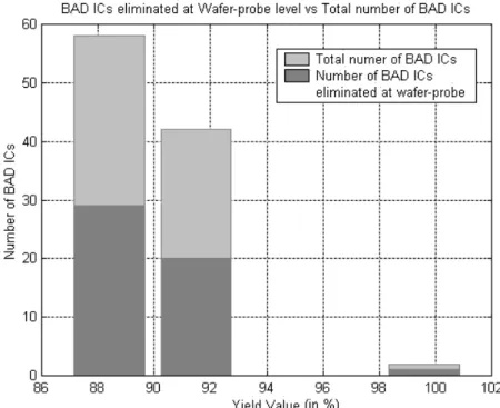
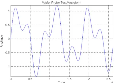
Figure 2.13. Comparison of bad ICs eliminated at WP vs. the total bad ICs. 35 Figure 2.14. Assembled package test waveform for Case Study I. 35 Figure 2.15. Wafer-probe test waveform for Case Study I. 36
Figure 2.16. AC Response of the DUT. 37
Figure 2.17. Assembled package test waveform for Case Study II. 38 Figure 2.18. Wafer probe test waveform for Case Study II. 38
Figure 2.19. Assembled package test waveform for Case Study III. 40 Figure 2.20. Wafer probe test waveform for Case Study III. 40 Figure 2.21. Assembled package test waveforms from hardware measurement. 42 Figure 2.22. Wafer probe test measurements made on the prototype. 42 Figure 2.23. Hardware prototype used for validation purpose. 43 Figure 3.1. Variation in process or circuit parameter and its effect on specification
and measurement. 50
Figure 3.2. Test selection algorithm. 52
Figure 3.3. (i) Band Pass Filter characteristics with input power = -20 dBm (ii) LNA Gain for input power = -30 dBm (iii) Receive mixer conversion gain with
input power = -30 dBm. 54
Figure 3.4. Single tone (200 KHz) spectrum received 55 Figure 3.5. Loopback test setup for testing the transceiver. 56 Figure 3.6. (i) Modulated waveform captured by NI Card (ii) Spectrum of the
captured waveform and (iii) zoomed in spectrum for the baseband 56 Figure 3.7. GMSK modulated spectrum at baseband (i) transmitted (ii) received. 57 Figure 4.1. Relation between the process, specification and measurement space. 62 Figure 4.2. Reduction of dimensionality of data using Principal Component
Analysis (PCA). 64
Figure 4.3. Flowchart showing test generation algorithm for process diagnosis. 66 Figure 4.4. Diagnosis core embedded in a bigger circuit. 67
Figure 4.5. Part of diagnosis core (mixer). 69
Figure 4.6. Pareto plot showing contributions by each principal component 70 Figure 4.7. The first two principal components on the new set of axes. 71
Figure 5.1. Pulsed-UWB Transmitter. 79
Figure 5.2. UWB receiver architecture. 79
Figure 5.4. Variation in sampled value with change in phase of the interferer
signal (for multiple power levels of the interferer). 83
Figure 5.5. Proposed production test setup. 85
Figure 5.6. Waveform of transmitted and received pulse. 86 Figure 5.7. Proposed test architecture using a pulsed RF signal generator. 88
Figure 5.8. MB-OFDM Frequency allocation. 89
Figure 5.9. UWB transmitter architecture. 90
Figure 5.10. UWB receiver architecture. 91
Figure 5.11. Standard EVM test setup. 91
Figure 5.12. Time domain OFDM signal transmitted. 93
Figure 5.13. CCDF plot of OFDM signal. 94
Figure 5.14. Standard CCDF test setup. 94
Figure 5.15. Standard BER test setup using a BERT. 96
Figure 5.16. Test cost model. 97
Figure 5.17. Relation between time domain input and FFT output. 100 Figure 5.18. Phase offset required vs. frequency of input stimulus. 101 Figure 5.19. Pseudo-code for generating test waveform. 103
Figure 5.20. Proposed EVM test setup. 103
Figure 5.21. Constellation diagram using proposed approach. 104 Figure 5.22. OFDM signal transmitted for proposed approach. 104
Figure 5.23. Proposed CCDF test setup. 105
Figure 5.24. Flowchart of genetic algorithm used for test generation for CCDF. 107
Figure 5.25. QPSK symbols for BER test. 109
Figure 5.26. Variations in interference PSD for different bands at the transmitter
antenna. 111 Figure 5.27. Repeatability test for victim I at UWB transmitter and victim 113
receiver.
Figure 5.28. Repeatability test for victim II at UWB transmitter and victim
receiver. 114 Figure 5.29. Simulation example: the transmitted and the received bits. 115 Figure 5.30. Simulation results with interference added. 115 Figure 5.31. BER performance of a UWB transceiver in presence on interference. 116
Figure 5.32. Estimating the error probability. 117
Figure 5.33. Comparison of repeatability for (i) standard and (ii) proposed test. 118 Figure 5.34. EVM constellation diagrams for a defective device using (i) standard
and (ii) proposed test methods. 119
Figure 5.35. ‘Golden CCDF curve’ generated from testing 1000 devices. 120 Figure 5.36. Comparison of the 'golden CCDF curve' and the CCDF curve from
the optimized bitstream, obtained from genetic algorithm. 120 Figure 5.37. Repeatability of CCDF curve using optimized bitstream as input
stimulus. 121 Figure 5.38. Detecting a faulty device using standard and proposed tests. 121 Figure 5.39. BER comparison for standard and proposed test for a Bluetooth
interferer. 122 Figure 5.40. EVM with varying SNR for standard and proposed test methods. 123 Figure 5.41. BER comparison for standard and proposed test for IEEE 802.11a
interferer. 123 Figure 5.42. EVM with varying SNR for standard and proposed test methods. 124 Figure 5.43. BER comparison for standard and proposed test for IEEE 802.15.4
interferer. 125 Figure 5.44. EVM with varying SNR for standard and proposed test methods. 125 Figure 5.45. Sales volume over five years: three possible trends. 127 Figure 5.46. Test cost/device for different sales trends. 127 Figure 5.47. Saving per quarter and overall savings using proposed test approach
Figure 6.1. BIT approach. 131
Figure 6.2. Schematic of LNA and VCO circuits. 132
Figure 6.3. LNA specifications estimated by using an external sinusoidal source 133 Figure 6.4. LNA specifications estimated using VCO output as test stimulus. 133 Figure 6.5. Spectrum of periodic and random bitstream. 136 Figure 6.6. GMSK baseband spectrum and PA output spectrum. 140 Figure 6.7. FSK baseband spectrum and PA output spectrum. 141
Figure 6.8. Sensors embedded in the DUT. 145
Figure 6.9. System test overview. 145
Figure 6.10. Sensors placed for system specification test. 146
Figure 6.11. Flowchart of core algorithm. 148
Figure 6.12. Percentage error in prediction of filter specification for different
process perturbations. 150
Figure 6.13. Percentage error in prediction of filter specifications for different
input test stimuli. 150
Figure 6.14. Test architecture for Case Study II. 151 Figure 6.15. Change in maximum error for Gain with number of input tones. 152 Figure 6.16. Change in maximum error for IIP3 with number of input tones. 152 Figure 6.17. Prediction of system specifications using sensor measurements. 154
Figure 6.18. Test architecture. 154
Figure 6.19. Receiver system with LNA and mixer. 155 Figure 6.20. Comparison of LNA results from netlist simulation and hardware
measurements. 156
Figure 6.21. Mixer hardware measurement results. 157
Figure 6.22. RMS detector schematic. 158
Figure 6.24 RMS detector circuit board. 159 Figure 6.25 Comparison between simulation and hardware results. 159 Figure 6.26. Receiver front-end with the sensors placed in the design. 160 Figure 6.27. Specification prediction using sensor outputs only. 162 Figure 6.28. Specification prediction using sensor outputs and IF output
waveform. 163 Figure 6.29. Fabricated receiver board for test purpose. 164 Figure 6.30. Input test stimulus to the receiver. 165 Figure 6.31. Output IF waveform from the receiver. 165 Figure 6.32. Comparison of actual specification values and the predicted
specifications (i) LNA gain (ii) LNA IIP3 (iii) Mixer gain and (iv) Mixer IIP3 166 Figure 6.33. Test setup used to emulate production testing 167
List of Tables
Table 2.1. Different components used for cost computation. 31 Table 2.2. Operating frequency and WP frequency limits for different devices. 33 Table 2.3. Accuracies achieved for different specifications (Case Study I). 33 Table 2.4. Comparison of test cost and ICs eliminated at WP test for different yield
values. 33
Table 2.5. Change in error in prediction with change in frequency limit of WP. 33 Table 2.6. Accuracies achieved for specifications. 37 Table 2.7. Comparison of test cost and ICs eliminated at WP test for different
yield. 37
Table 2.8. Accuracies achieved for specifications. 39 Table 2.9. Test cost and ICs eliminated at WP test. 39 Table 2.10. Accuracies achieved for specifications. 43 Table 2.11. Test cost and ICs eliminated at WP test 44 Table 2.12. Cost comparisons for proposed algorithm and standard test (Case
Study I). 44
Table 2.13. Cost comparisons for proposed algorithm and standard test (Case
Study II). 44
Table 2.14. Cost comparisons for proposed algorithm and standard test (Case
Study III). 45
Table 2.15. Cost comparisons for proposed algorithm and standard test (Case
Study IV). 45
Table 3.1. Module characterization data from hardware. 53 Table 3.2. Receiver and transmitter characterization data. 53 Table 3.3. Specification predicted from hardware data. 58 Table 4.1. Process parameters and their accuracies. 70
Table 5.1. QPSK Modulation (generating I and Q values). 92 Table 5.2. Required tester specifications for UWB devices 98 Table 5.3. Test cost values considered for analyzing standard test method. 98 Table 5.4. Required tester specifications for UWB devices. 110 Table 5.5. Test cost values considered for analyzing the proposed test method. 110 Table 5.6. Interference PSD at different bands (victim I and victim II). 112 Table 5.7. Comparison of standard and proposed test methods. 118
Table 5.8. Test-time savings. 118
Table 5.9. Test-time savings for BER = 0.001. 126
Table 5.10. Test-time savings for BER = 0.0001. 126
Table 6.1. LNA specification prediction. 133
Table 6.2. Comparison of bit-sequence length and accuracy (GMSK). 138 Table 6.3. Comparison of bit-sequence length and accuracy (FSK). 140 Table 6.4. Comparison of bit-sequence length and accuracy (FSK). 142 Table 6.5. Comparison of bit-sequence length and accuracy (FSK). 142 Table 6.6. Error in prediction of system as well as module specifications using
sensors 153 Table 6.7. Error in prediction of system as well as module specifications using
sensors 153
Table 6.8. Individual module specifications. 155
Table 6.9. Performance comparison of the receiver with and without sensors. 161 Table 6.10. Gain prediction using single-tone test for the receiver. 162 Table 6.11. IIP3 prediction using 2-tone test for the receiver. 162 Table 6.12. Specification prediction results from the receiver board from the
sensor output response measurements. (In addition, actual specifications were measured using standard specification test methods, with sensors built-into the
Table 6.13. Mean, maximum and minimum error values in prediction using the
Summary
Testing is an integral part of modern semiconductor industry. The necessity of test is evident, especially for low-yielding processes, to ensure Quality of Service (QoS) to the customers. Testing is a major contributing factor to the total manufacturing cost of analog/RF systems, with test cost estimated to be up to 40% of the overall cost. Due to the lack of low-cost, high-speed testers and other test instrumentation that can be used in a production line, low-cost testing of high-frequency devices/systems is a tremendous challenge to semiconductor test community. Also, simulation times being very high for such systems, the only possible way to generate reliable tests for RF systems is by performing direct measurements on hardware. At the same time, inserting test points for such circuits while maintaining signal integrity is a difficult task to achieve.
The proposed research develops a test strategy to reduce overall test cost for RF circuits. A built-in-test (BIT) approach using sensors is proposed for this purpose, which are designed into high-frequency circuits. The work develops algorithms for selecting optimal test access points, and the stimulus for testing the DUT. The test stimulus can be generated on-chip, through efficient design reuse or using custom built circuits. The test responses are captured and analyzed by on-chip sensors, which are custom designed to extract test response features. The sensors, which have low silicon area overhead, output either DC or low frequency test response signals and are compatible to low-speed testers; hence are low-cost. The specifications of the system are computed using a set of nonlinear models developed using the alternate test methodology. The whole approach has been applied to a RF receiver at 1 GHz, used
as a test vehicle to prove the feasibility of the proposed approach. Finally, the method is verified through measurements made on a large number of devices, similar to an industrial production test situation. The proposed method using sensors estimated system-level as well as device-level specifications very accurately in the emulated production test environment with a significantly smaller test cost than existing production tests.
Chapter I
Introduction
Chapter 1
1.1. Standard Industry testing approach
The standard industrial test development flow for any commercial product is shown in
Figure 1.1.
Figure 1.1. Industrial test development flow. Design and layout of
silicon by designers Product description from market
survey or specific customer
Fabrication of device
Define test requirements depending on the customer
Generate test plan for the device/product Decide upon tester, develop test program for
the device/product Bench test and characterization
of the device
Perform tests on tester. Take care of issues related
to test ordering, accuracy and repeatability. Test
program debugging Performance satisfactory? Production test Yes No
First, after the market demand has been studied and customers of the specific product
have been well identified, the test development process is started. Usually, there are two
different types of test requirements. For any product specially requested by a specific
customer, the stringent specification requirements depending on application targeted by
the customer, decides the tests that need to be performed to meet these necessities. For
other types of products, where the manufacturer targets a new segment of the market with
a solution to the needs of the consumers, the manufacturers themselves usually set the
test requirements. Once the test requirements are identified, the test engineers work with
the designers to generate the test plan for the device or product. As the device goes into
production manufacturing, test engineers decide upon the tester to use depending on the
test requirements and the resources available from different testers. In addition, the test
program for production test is also developed. In addition, the device load board is
designed and simulated during this time.
As soon as the fabricated devices come back from fabrication, first, a bench test is
performed to characterize the product, understanding the silicon behavior, as well as
detecting any unforeseen problems that might be associated with the fabrication and
design. Once the device performs satisfactorily in the bench test, the load board is sent
for manufacturing by the test engineer. Next, the challenge for the test engineers is to
make the test program functional for production test, which involves debugging and
restructuring the tests to obtain similar performance as obtained in the bench or close to
it. In addition, issues related to loss in accuracy and errors from the tester and its
associated accessories need to be considered here, and it is desired to have no loss of
determines the issues related to repeatability and the handlers/ wafer probers. Once the
program is debugged and the device specifications can be measured with a very small
error margin, the test programs are released for production testing.
1.2. Problems and possible solutions
In general, for any device, there exist tests that are similar in nature, exercising the
same behavior of the device under test. Tests, viz. IIP3, and 3rd Harmonic measurements are similar in nature, but usually to ensure uncompromised performance of the device, in
some cases, these tests are performed separately. Moreover, the test procedure in industry
is essentially sequential. With this approach, the test time is undoubtedly longer than it
should be. Several approaches, as discussed below, are taken to reduce the number of
tests, as well as the overall test cost.
1.2.1. Test compaction
In this approach, the tests are usually combined together to perform multiple tests with
a single data capture operation. This method is applied to cases where the specifications
of the devices need not be measured very accurately. In such cases, reduction of the
overall test time to reduce the manufacturing cost plays a vital role, while the loss of
accuracy in measurements up to certain limits is not critical to ensure device
performance. The results of all the associated tests are calculated from the acquired data
with the aid of mathematical equations that relate the results of the different tests to the
measurements made. Usually, these equations are incorporated within the test program to
1.2.2. Test parallelization
While test compaction is performed with the aid of equations relating different
specifications to a single measurement, test parallelization incorporates the technique
where many parts of a large circuit can be tested in parallel, at the same time. This
method, contrary to the method described above, uses multiple measurements to test
individual specifications and is thus more accurate. Tests, viz. PSRR and Gain for
OpAMP, can be performed in parallel using this approach.
1.2.3. An overview of alternate test
In the alternate testing approach, the test specifications of the circuit-under-test are not
measured directly using conventional methods (such as circuitry and stimulus to measure
CMRR, for example). Instead, a specially crafted stimulus is applied to the
circuit-under-test and the (conventional) circuit-under-test specification values are computed (predicted) directly
from the observed test response. Test generation for this approach starts with the standard
test plan for any product and the test generation algorithm. Usually, sample sets of
devices are chosen from different lots and are then used in test generation, as shown in
Figure 1.2. The final output from the test generation approach is the optimized test
stimulus, which potentially replaces all the specification tests for which the test
generation was performed. During test, this optimized test stimulus is applied to the DUT
and from the response of the DUT, the specifications are estimated directly with a very
small margin of error. In general, all the test specifications can be computed from the
response to a single applied test stimulus or a set of stimuli applied to the different ports
Figure 1.2. Alternate test generation framework.
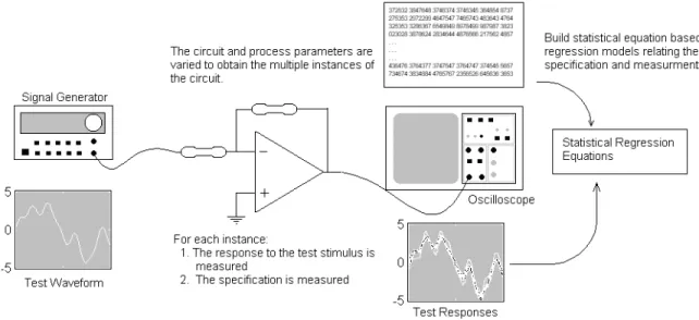
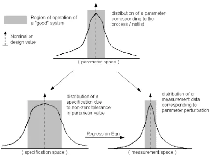
1.3. Alternate test fundamentals
Alternate test has been around for a long time since Variyam and Chatterjee proposed
it in 1998 [42]. Alternate test, as of today, seems to be the only viable solution to the
problem associated with testing high-frequency devices. As described in section 1.2.3,
alternate test makes use of the variations in the response of the DUT to estimate the
specifications, even without performing any standard test procedure. It is a manifestation
of test compaction, test ordering and use of inherent statistical correlation between the
process parameters and the specifications. Though, today the concept has been extended
to different directions [15],[44],[102],[103],[47],[48],[119],[120], the core idea remains
the same.
Design and optimize the test stimulus
using desired algorithm
Select sets of devices to be used for alternate test
generation
Measure the specifications of interest using standard test method for all devices
Apply customized waveform to the devices
and capture responses
Figure 1.3. Alternate test generation.
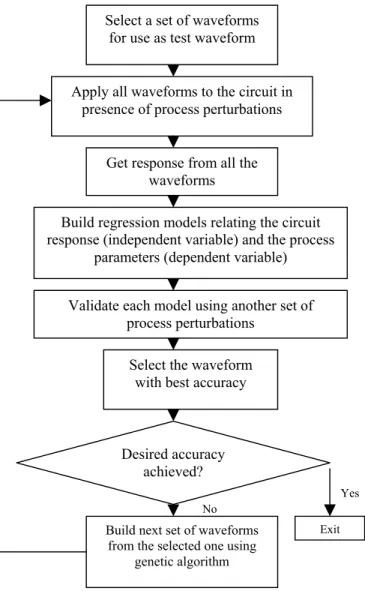
Figure 1.3 shows the idea behind generation of alternate test. During test generation,
various waveforms, generated using sinusoids, pulses, piecewise linear and a
combination of some or all of those, are considered. Each of the waveforms is considered
individually. For each waveform, as shown in Figure 1.3, multiple instances are
generated for the device-under-test. For each instance, the response to the input
waveform is captured and stored, and, at the same time, the specifications of interest are
measured using the standard specification measurement technique. After this procedure is
finished for all the instances, the responses and the measured specifications are related
using non-linear regression equation, which is referred as model. Thus, models are
constructed for all the candidate waveforms. Next, the accuracy of the models is
evaluated using a set of test inputs. In some cases, the candidate waveform is picked
directly depending on accuracy of the models, or the waveforms are further optimized to
obtain better accuracy. Finally, the optimized test waveform is produced. This optimized
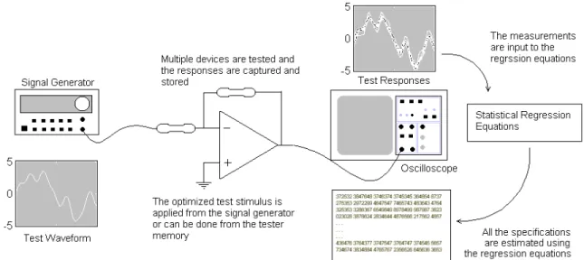
Figure 1.4. Application of alternate test to estimate specifications.
After the test is generated, the test is applied to the devices to be tested. The optimized
test waveform is applied to each device and the output response is captured. The
measured response is then put into the model that was generated, as shown in Figure 1.4,
and the model outputs the specifications of the circuit. This procedure does not require
any other tests to be made on the circuit and all the specifications can be obtained directly
from the model.
1.3.1. Use of alternate test
The alternate test approach, described above, is compact and easy to use with any
device. With the test times for different complex devices being very high and with a very
little possibility of test compaction or parallelization, alternate test can use a single test
stimulus to test all the specifications, thereby simplifying load-board designs
considerably. Moreover, test time is very less compared to standard specification tests.
assembled-package and wafer-probe are co-optimized using alternate test to reduce test
cost.
1.4. Contributions
This section briefly summarizes the contributions and the novelty of this thesis. Figure
1.5 summarizes the contributions in different classes of electronic devices. It can be
broadly divided into three classes. Initial part of the thesis focuses on co-optimizing tests
for wafer probe and assembled package devices. This method has been validated on
OpAMPs, high-speed comparators and a RF mixer. In addition, this was validated
through hardware measurements performed on OpAMPs.
Next part focuses on test development of RF devices. Initially, to ease simulation
constraints, behavioral models were built for devices, viz. LNA, mixer as well as
front-end RF sub-systems. After the initial learning phase, a loop-back test methodology was
proposed with the objective of built-in-test of RF systems. A hardware validation of the
proposed approach was performed. However, limitations of the loop-back test were later
understood and a built-in-test approach using sensors was proposed as the thesis topic. A
receiver system with sensors was built to validate the method.
The other class of devices investigated was ultra-wide band (UWB). For this class, test
methodologies to reduce test time and test cost for both pulsed and MB-OFDM devices
were proposed.
The following chapters elaborate the different methods developed for enhancing
production test of electronic devices by reducing test cost and test time using alternate
Chapter II
Wafer-Probe and Assembled-Package Co-optimization
to Minimize Overall Test Cost
Chapter 2
Because of the increasing complexity and speed of analog, mixed-signal, and RF ICs,
test engineers are often faced with characterization and new production testing challenges
to ensure high product quality without incurring excessive testing costs. In a typical IC
manufacturing process, first the bare die on each silicon wafer are tested using a
wafer-probe tester. This procedure is called the wafer-wafer-probe (WP) test. Subsequently, the
“good” die are diced, packaged and tested again; a procedure, known as the assembled
package (AP) test, is performed to eliminate any bad ICs passed by the wafer-probe test
procedure. In this work, the objective is to reduce the overhead of the AP test to bring
down the overall test cost.
2.1. Previous work
In the past, there has been significant effort in the area of reducing specification testing
time by eliminating unnecessary tests and ordering them in an optimal way [1]. However,
these tests are still time consuming and expensive. In [2], the authors propose using extra
tests during wafer-probe testing to eliminate faulty packaged circuits. In [3], the authors
proposed a way to generate tests for analog circuits using fault models. Nagi et al,
presented a test frequency selection algorithm in [4] for AC testing using behavioral-level
fault modeling. In [5], a test-generation algorithm for detecting single and multiple faults
based on circuit sensitivity computation was presented. In [6], the authors solved the test
digital test generator tool to obtain test stimuli for analog circuits. In [8], Tsai showed
that the difference between faulty and fault-free circuits could be maximized using a
quadratic programming-based transient test optimization procedure. Abraham, Chen, and
Balivada [9] used a ramp as the primary test stimulus for analog circuits.
The process of alternate testing consists of applying a short transient test stimulus to
the circuit under test (CUT) and analyzing the corresponding (sampled) test response to
predict the circuit’s specifications. In the alternate testing approach, the test specifications
of the CUT are not measured directly using conventional methods (such as circuitry and
stimulus to measure CMRR, for example). Instead, a specially crafted stimulus is applied
to the CUT and the (conventional) test specification values are computed (predicted)
from the observed test response. In general, all the test specifications can be computed
from the response to a single applied test stimulus.
In [10], [11], and [12], the authors presented an assembled package test method that
relies on the application of a carefully designed transient test stimulus for implicit
specification testing of analog ICs. In this approach, the specification values of the device
under test (DUT) are predicted from the response of the DUT to the applied test stimulus.
This approach is not directly applicable to wafer-probe testing, as the signal drive and
response observation capabilities during wafer-probe testing are limited because of
parasitics from long cables and probes used in the procedure. Moreover, the various test
cost components of wafer-probe and assembled-package testing need to be considered
concurrently to get the maximum benefits from both tests and to construct an optimal
wafer-probe and corresponding assembled-package test program that minimizes overall
during test generation. Later, in [14], they used nonlinear regression models to predict the
specifications from the responses for both assembled-package and wafer-probe testing
and co-optimized the tests for wafer-probe and assembled-package testing. In [15] and
[16], the authors showed that this method can be applied to high-speed devices as well
and excellent accuracy can be achieved using the proposed test methodology.
2.2. Predicaments in wafer-probe testing
During wafer-probe testing, the tester makes an electrical contact with each die on the
wafer through traveling probes that touch down on the die pads. Because of the long
cable lengths and Schottky contacts formed by the probes at the die surfaces, huge
parasitics are introduced in the signal path. For this reason, typically for analog circuits,
DC tests and power supply current tests are performed during the WP test. All other
specifications are measured during AP test, i.e., slew rate, gain, noise figure, etc. The
electrical performance (parasitics) of the probe is modeled using a passive network and is
referred to as the "wafer-probe model" in Figure 2.1. Such a passive network for an
industrial wafer-probe tester is shown in the next section. The parasitics added to the
input of the DUT in Figure 2.1 by the probe contact limit the signal that can be applied to
the DUT. The same parasitics connected to the output of the DUT limit the external tester
observation capability of the response to the applied stimulus. Similarly, during AP
testing, the signals that can be seen by the CUT are limited by the package parasitics,
while the small amount of parasitics introduced by the load board and the signal traces
can be ignored. Package models associated with the inputs and outputs of the CUT are
used to model the constraints as a result of test signal application and device response
Figure 2.1. Models used for WP and AP test setups.
2.2.1. Solutions
In this approach, instead of finding a way to overcome the above problems associated
with the parasitics, the parasitics are modeled very carefully and accurately. Thus, their
effects are taken into account during test generation, and optimization is performed.
2.3. Co-optimization framework
During test stimulus generation, the suitability of a candidate test stimulus for a WP or
AP test is evaluated by simulating the circuit under test using the associated end-to-end
models, as shown in Figure 2.1. The objective is to be able to evaluate the performance of
the embedded circuit under test by observing the output of the corresponding model of
Figure 2.1 (these are the signals seen by an external tester). Furthermore, the goal is to
detect as many bad die as possible during WP testing, even when the signal drive limitations imposed by the WP model are significant. As an extreme example, the circuit
under test may be a 1 GHz device, while the wafer probe may be "good" only up to
300-400 MHz. WP and AP parasitic models for the HPL-94-18 Tester and a DIP40 ceramic
Figure 2.2. Wafer-probe model.
Transient tests are used during production testing for both WP and AP methods.
Transient tests can be designed to extract a maximum amount of information about the
DUT even when WP performance is not as accurate as compared to that of the circuit
under test. In this way, a significant number of bad ICs can be detected during
wafer-probe testing. Further, given the test cost components of the wafer-wafer-probe and assembled
package test procedure, new algorithms can be developed for co-optimizing wafer-probe
and assembled package tests to minimize test cost and test time, while ensuring high
coverage and improving yield. Figure 2.4 shows the test framework used in industry for
pass/fail binning of the circuits/devices.
Figure 2.4. WP and AP test framework.
In the proposed approach, given the WP test cost/sec, AP test cost/sec, process
minimize the overall test cost. For WP test stimulus evaluation, WP parasitic models are
used and for AP test stimulus evaluation, AP parasitic models are used. The optimal tests
are obtained by co-optimizing the WP and AP test stimuli. Moreover, the proposed
algorithm can be configured to accommodate any relation between WP and AP test costs.
Using different test cost values for a specific device might result in a different waveform
with different duration, but the proposed method of co-optimization remains the same. As
already explained, the WP test cost/time is usually less than the AP test cost/time.
2.4. Test approach
In the case of WP testing, traveling probes test the whole die, and there is very little
mechanical movement involved (stepping time is approximately 120 ms) [17]. In AP
testing, every time a new chip needs to be tested, it is put into the test site by a handler,
followed by sorting and putting it into the correct bin, depending on the outcome of the
test (total time required for handling is 300 ms, indexing time being 150 ms) [18]. This
involves a lot of extra mechanical movement and causes an increase in the test
cost/second for AP. Thus, the WP test cost per second (approximately 1.5¢/s) is
significantly less than the AP test cost per second (approximately 5¢/s). Therefore, bad
ICs detected during wafer-probe testing can help reduce the overall test cost dramatically.
During production testing, all bad ICs that pass the WP test are packaged for AP testing
and are eventually discarded after the AP test. A good WP test procedure minimizes the
number of such bad ICs that are packaged and retested. On the other hand, WP test times
that are too long (~5× AP test time) can offset the advantages of WP testing.
In our proposed test-generation approach, one-time establishment costs for wafer probe
bring down the production test cost. Several studies concerning the cost of probes and
handlers to reduce overall test cost have been performed by various researchers, but in
this work, the focus is on reducing the overall manufacturing cost by minimizing the
functional test costs by reducing test times and packaging costs by eliminating bad
devices at an early stage of production test.
The results of the WP (transient) test and AP (transient) test are mapped to the test
specifications of the packaged ICs for pass-fail decision. Test guard bands are set so that
all good ICs pass the WP test. A few bad ICs that pass the WP test are eventually
detected during the AP test. The guard bands for the assembled package testing are set in
such a way that all bad ICs are detected by the test. Some yield loss may occur by using
the proposed test procedure because of a few good ICs being classified as bad, but this
ensures that the test coverage remains very high and is able to detect all the faulty ICs.
2.5. Fault model
In our approach, the process parameters (i.e., device width, length, oxide thickness,
zero-bias threshold voltage, etc.) are varied to generate different instances of the DUT.
The process parameters are varied according to a statistical distribution (assuming a
Gaussian distribution) to mimic the actual manufacturing process using the mean and the
standard deviation values. The parametric variations are modeled as shown in Figure 2.5.
For each such combination of process parameters, the specification value is computed
Figure 2.5. Parametric fault modeling.
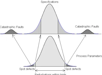
This work focuses on functional test generation for the DUT. Random or spot defects,
which are manifestations of catastrophic faults, i.e., open, short, or bridging faults, cause
large deviations from the nominal specification values (Figure 2.5). Therefore, any spot
defect present in the DUT will affect the response to the optimized input waveform
considerably, resulting in a grossly inaccurate estimation of specification(s). In such a
case, the DUT will lie outside the test limits imposed by the test engineer. Thus, using the
proposed algorithm, any DUT with spot defects will definitely be eliminated. In another
case, there might be some spot defects present that do not affect the specifications or the
test response at all (or affect it by a very small amount). This essentially means that the
specific spot defect is not affecting the DUT performance in any way. Thus, the proposed
algorithm can handle the effect of spot defects although they are not generated as a part
2.6. Test algorithm
The DUT performance parameters are directly related to the process parameters. While
all the process parameters affect the DUT performance in some way or other, considering
a smaller “critical” set of process parameters that bears high correlations to the
specification values can perform accurate test generation. Identifying this set of “critical”
parameters is necessary to reduce the simulation complexity of the test generation
algorithm. So, before the test-generation process starts, a search algorithm is used to find
the critical process parameters. Section 2.6.1 describes the algorithm for identifying these
process parameters.
2.6.1. Computing critical process perturbations
For given process statistics, N process vectors, each consisting of different assignments
of the n process parameters, [p1, p2, … pn], can be generated using statistical sampling.
For this purpose, the process parameters are varied around a mean value, with a specific
standard deviation, and the process and circuit parameter vectors are generated in such a
way that they cover the whole process space within the standard deviation limits. These
process vectors (that impact the DUT’s performance) are applied to the DUT, and
corresponding sets of m specification values of interest constituting the specification
vector [s1, s2 … sm] are measured. Hence, N specification vectors are generated,
corresponding to each of the N process vectors.
Once the process parameter and specification vectors are generated, nonlinear
modeling using multivariate adaptive regression splines (MARS) [19], explained in
models generated, critical process parameters are identified following a greedy search
algorithm, as explained in Section 2.6.1.2.
The relation between the responses of the DUT and the specifications is nonlinear.
Using a simpler modeling option, e.g., Taylor series expansion, for constructing the
models may not capture all the nonlinear relationships between the responses and the
specifications. For the above-mentioned reason, MARS was used for modeling.
2.6.1.1. MARS model generation
MARS are used for developing the nonlinear model that relates the process parameters
to the DUT’s test specifications. The MARS algorithm mainly depends on the selection
of a set of basis functions and a set of coefficient values corresponding to each basis
function to construct the nonlinear model. The model can also be visualized as a
weighted sum of basis functions from the set of basis functions that spans all values of
each of the independent variables. MARS use two-sided truncated functions of the form
(t-x)+ and (x-t)+ as basis functions for linear and nonlinear relationships between the
dependent and independent variables, t being the knot positions. The basis function has
the form as shown in (1).
−
>
=
−
otherwise
t
x
t
x
t
x
0
)
(
(1)The basis functions together with the model parameters are combined to generate the
model, which can predict the dependent variables from the independent variable values.
The MARS model for a dependent variable y, independent variable x, and M basis
functions, is summarized in (2).
∑
= + = = M m m k v km mH x x f y 1 ) , ( 0 ( ) ) ( β β (2)where the summation is over the M independent variables, and β0 and βm are parameters of the model (along with the knots t for each basis function, which are also
estimated from the independent data). The function H is defined as
∏
= = K k km m k v km x h H 1 ) , ( ) ( (3)where xv(k,m) is the kth independent variable of the mth product. During the forward stepwise placement, basis functions are constantly added to the model. After this
implementation, a backward procedure is applied when the basis functions associated
with the smallest increase in the least squares fit are removed, producing the final model.
At the same time, the generalized cross validation error (GCVE), which is a measure of
goodness of fit, is computed to take into account the residual error and the model
complexity. The above equation can be further decomposed into the sum of linear, square
products, cubic products, and so forth. Introducing a larger or smaller number of basis
functions can also change the accuracy. Changing the order of products can change the
degree of nonlinearity of the model.
2.6.1.2. Selection of critical process parameters
As described above, a nonlinear mapping from the n-dimensional process vector space
(∆p) to the m-dimensional specification vector space (∆s) is constructed using MARS, as shown in (4).
( ) ( )
p
p
s
=
Ψ
∆
⋅
∆
∆
(4)A set of critical process parameters is identified using a greedy algorithm-based search
method. First, one set process vector and the corresponding specification vector is
( )
∆s ′ = Ψ ′(
∆p′) ( )
⋅ ∆p ′ (5) N such models are created, each time eliminating one process vector and thecorresponding specification vector. Each model is then used to predict the eliminated
specification vector by using the corresponding eliminated process vector, used as the
input to the model. Next, the error between the estimated and the actual specification
vector is computed. The process vector, the exclusion of which produces the largest error,
is considered the most critical process parameter vector. The eliminated process vectors,
for which the corresponding model produces error values above a certain threshold, are
selected as “critical vectors.” The algorithm is shown in Figure 2.6.
function Selection(P,S,k) P = Process matrix (N X p);
S = Specification matrix (N X s);
p = Number of process and circuit parameters; s = Number of specifications;
N = Total number of process vectors; k = Number of critical process vectors;
for i = 1,2 … s { Svalidation = S(i,:); Ptemp = P; Stemp = S; for x = N, (N-1) … (N-k+1) { for j = 1,2 … x { Pvalidation = Ptemp(j,:); Svalidation = S(j,:);
Preduced = Ptemp - Pvalidation;
Sreduced = Stemp - Svalidation;
Mj = BuildMARSModel(Preduced, Sreduced);
Error(j) = Svalidation – EvalMARSModel(Mj,Pvalidation);
}
Index = maxIndex(Error); /*returns index for maximum error */
Append(CriticalProc(i), Ptemp(Index));
Ptemp = Ptemp – CriticalProc(i);
} }
return CriticalProc;
2.6.2. Core algorithm
During the manufacturing process, as devices are fabricated, there is no way to get
access to the process data unless measurements are made on the device after
manufacturing. Thus, after manufacturing, one does not know the process data and hence
there is no knowledge about the process and circuit parameters. Therefore, we cannot use
a methodology to get the specifications directly from the process and circuit parameters.
The process parameters were varied to generate different instances of the DUT to
mimic the actual manufacturing process. However, in an actual manufacturing process,
all the process parameters vary around the nominal value, with a specific statistical
distribution. In simulation, it is nearly impossible to vary all the process parameters. So,
first a set of critical process parameters was selected. For example, the selected process
parameters included oxide thickness, width, and length of the MOS devices. Initially, k
critical process perturbations are computed for all the specifications, as described in
Section 2.6.1. The algorithm starts with a set of N waveforms and a set of k critical
process vectors. The initial choice of waveforms is random, where several candidate
waveforms, i.e., sine waves, pulses, and piecewise linear waveforms, or a combination of
those, are used as a preliminary guess for both WP and AP tests. These are successively
co-optimized to generate the final test waveform.
First, the test waveforms for the WP test and AP test are constructed independently,
depending on the frequency and current limitations of each test setup. N such pairs of
waveforms, for WP and AP, are constructed, which are treated as the initial population
space for co-optimizing. All the test waveforms are applied to the DUT while the circuit
critical process variations to obtain the corresponding k response waveforms. The
specifications of the DUT under each of the k process variations are already computed
while calculating the critical process vectors. From the data, a MARS model relating the
sampled response waveform to the DUT’s specifications is constructed (given the
response waveform, the model computes the DUT’s specification values). This is done
separately for the WP and AP test waveforms. Let us denote the model relating the WP
responses to the specifications by MWP and the model relating the combined WP and AP
responses to the specifications by Mcomb. For each WP and AP test waveform set, two
such models are created. The process is described in Figure 2.7.
Now, the fitness of each of the models (MWP and Mcomb) is found from a set of
reference process vectors and their corresponding specification values, which are also
computed beforehand. By using these process vectors to perturb the DUT instances, the
test waveforms are applied to the DUT and the response obtained is used as the input to
the model. From the response and the model, estimates of the specifications are obtained.
These are then compared to the actual values, and errors are computed for each model.
The error between the specifications predicted from the model and the actual
specifications obtained from the circuit measurements serve as the fitness of the model.
The error can be obtained as shown in (6).
( )
( )
∑
= − = S j N predicted N actual NN Spec j Spec k j S k Spec 1 , 1 ) ( for ∀k∈{
1,K,N}
(6)where, k indicates the stimulus currently being considered, SpecN
actual(j) is the normalized specification computed for the reference process vectors, and SpecNpredicted
(k,j) is the normalized specification predicted by the model made from the circuit output
response measurements with all the process variations applied for the same stimulus. j
represents the index for normalized specification value, which is computed as shown in
(7). With those error values, the cost is computed, which is described in Section 2.7.
∑
= = P i N Spec i j P j Spec 1 ) , ( 1 ) ( (7)After the cost for all the waveforms is computed, the waveform that gives the least cost
is chosen and is used to evolve the next set of waveforms using a genetic algorithm.
Genetic algorithm comes in handy for optimization [20], [21]. It generates the optimized
waveform for specification prediction and searches the solution space of a function using
simulated evolution, i.e., survival-of-the-fittest strategy. In general, the fittest individuals
improving successive generations through mutation, crossover, and selection operations
applied to individuals in the population. An outline for a generalized genetic algorithm is
shown in Figure 2.8.
a) Supply a population P0 of N individuals and respective function values. b) i Å 1. c) Pi’ Å selection_function (Pi-1) d) Pi Å reproduction_function (Pi’ –1) e) evaluate(Pi) f) i=i+1
g) Repeat step 3 until termination
h) Output the best solution
Figure 2.8. Genetic algorithm framework.
To keep track of the test generation procedure and the fitness of the test, a few past
cost values are stored. More and more time points are added according to the changes in
the cost as the test progresses. The algorithm for modifying the test waveforms is shown
in the following pseudo-code in Figure 2.9.
Backtrack (CostHistory, Cost) /* change the waveforms */ /* Cost is the present cost value */
/* CostHistory is a FIFO vector of k past cost values */ /* CostHistory (1) contains the most recent cost value */ {
if CostHistory(1) > Cost & … & CostHistory(k) > Cost Increment wafer-probe waveform by one time step;
else
/*Cost is not improving by increasing the WP test waveform */ Backtrack 'k' time steps in WP test waveforms;
Increment the AP waveforms by one time step;
end if
Shift CostHistory by one position by discarding the oldest value
CostHistory(1) Å Cost; }
return;
2.7. Optimization cost function
In the proposed algorithm, shown in Figure 2.10, the test engineer provides these
specification limits before the test generation is started. During testing, these
specification limits are used to make a pass/fail decision about the circuit-under-test.
Before describing the cost function and its various parts, different features that constitute
the cost function and that must be taken into account, are described. The test cost has the
following components:
• Wafer-Probe Test Time (WPTT) × Wafer-Probe Test Cost/time (WPTC).
• Assembled-Package Test Time (APTT) × Assembled-Package Test Cost/time (APTC).
• Cost incurred because of the packaging of bad ICs after wafer-probe test, but which are actually detected by assembled-package test and eventually rejected.
• Cost incurred because of good ICs being considered as bad after final tests.
As described in Section 2.6.2, the DUT is simulated in the presence of critical process
vectors and testing is performed for both WP and AP. The measured specifications of the
DUT and the test responses from WP and AP are used to build models, MWP and Mcomb,
respectively. Let us define the errors obtained from the models MWP and Mcomb as Error
and WPError, respectively. These errors are used to compute the areas, designated as α,β
and γ in Figure 2.11, each of which is described in the next few paragraphs. ‘N’ denotes the total number of ICs tested. The picture shown in Figure 2.11 shows the distribution
(Gaussian) of specifications for any typical manufacturing process. The total area under
the graph represents the total number of ICs that are considered for test purposes. During
multiplied by the total number of ICs tested, as shown in (8), to obtain the number of ICs
that fall within that category.
Total Type Area Area TotalICs NumICs= × (8)
The first part of the test cost is the cost incurred because of the test time involved in
wafer-probe testing. The total test time for wafer-probe testing multiplied the wafer-probe
test cost per unit time gives the wafer-probe test cost. All ICs with specifications outside
the specification limits are considered bad. However, in this case, a certain uncertainty is
introduced because of the errors in the models, as described in Section 2.6.2. The errors,
Error and WPError, indicate the relative error present in the prediction process.
Therefore, any IC with a predicted specification value exactly at the specification limit
can have the predicted specification anywhere between ±WPError around the
specification limit.
Hence, there is an equal chance of that IC being good or bad and therefore it cannot be
classified completely. However, if the predicted value itself is at Specification limit +
WPError, then definitely the IC is bad. Therefore, all ICs with predicted values equal to
and above Specification limit + WPError are considered bad. This area in Figure 2.11
represents the ICs eliminated during wafer-probe testing and the number of bad ICs is
computed using (8). The ICs that have their specification values within the Specification
limit and the value Specification limit + WPError are actually bad ICs, but they are
packaged and passed on for assembled-package testing. Thus, the cost of packaging these
ICs is an unwanted cost brought on by test inaccuracy, i.e. the error in prediction of MWP.
This cost is included in the overall test cost. The area β in Figure 2.11 allows us to calculate the number of bad ICs that are packaged.
Figure 2.11. Distribution of specification used to compute test cost.
Finally, because of inherent errors in the test procedures, generally, test engineers set
the specification limits tighter than the ones set by the designers. This is to ensure that
despite the inaccuracies in measurements during testing, all bad ICs are definitely
eliminated. However, at the same time, some good ICs are eliminated because of the
tighter limits. This adds to the overall test cost. In this case, the test limit is determined
from the overall Error. The test limit is set to Specification Limit − Error. Using the area
γ in Figure 2.11, the number of good ICs that are rejected can be found. From the above discussion, the total test cost is obtained using (9).
Cost = WPTT XWPTC X N + Packaging Cost per IC X βN + APTT X APTC X (1— α) X N + Cost Of Individual IC X γN (9)
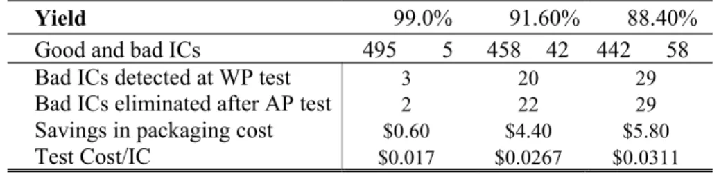
2.8. Results
In the following, results obtained from the developed prototype are presented using the
cost function and the optimization [22] approach as per the algorithm of Figure 2.10 [23].
The designs made for this work were developed with references from [24] and [25]. Also,
Results obtained from simulations for three circuits are presented below. The first
example (Case Study I) shows an experiment to demonstrate that a significant number of
bad ICs can be detected even when the cut-off frequency of the wafer probe is less than
the bandwidth of the DUT. The second example (Case Study II) shows results for a
high-frequency amplifier. The final example is a RF mixer (Case Study III). The DUT cost and
the packaging cost for each IC and the test time for each of the ICs using standard
specification testing are shown in Table 2.1. The test cost for the WP test was 1¢/s and
3¢/s for the AP test. Using these values, the test cost for standard specification testing
was computed.
Altogether, 500 ICs of each type were considered for test generation and validation
purposes. A large number of devices are used to ensure a proper statistical sampling. The
test cost data was obtained from industry members of the Semiconductor Research
Corporation (SRC) [27]. Case Study IV involved the validation of the proposed WP and
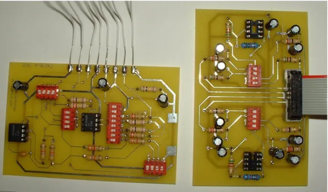
AP test methodologies using hardware measurements made on the National
Semiconductor LM318 operational amplifier [28].
Table 2.1. Different components used for cost computation.
Cost component Value used Case Study I Final product cost $0.50
Packaging cost $0.20 WP test time 150ms AP test time 500ms
Case Study II Final product cost $0.50 Packaging cost $0.35 WP test time 350ms AP test time 750ms
Case Study III Final product cost $1.50 Packaging cost $0.50 WP test time 1.8s AP test time 4s
Table 2.2 shows the different operating frequencies of the devices and the frequency at
which they are tested using the proposed methodology. The wafer-probe cut-off
frequency is the frequency up to which the signals applied to the probe station are not
distorted. This is caused by the parasitics introduced by long cables and sharp contact
probes used during WP testing. These introduce current and frequency limitations on the
signals and distort high-frequency signals considerably before they reach the device. The
input corner frequency is the maximum frequency at which the device can operate
without any introduction of nonlinearity into the signal.
Table 2.2. Operating frequency and WP frequency limits for different devices.
Operating frequency Test frequency
OpAMP 500 kHz 200 kHz
Comparator 250 MHz 50 MHz
Mixer 900 MHz 100 MHz
Hardware measurement 10 kHz 2.5 kHz
2.8.1. Case Study I
This circuit was designed and used as the circuit-under-test. The bandwidth of the
amplifier was close to 500 kHz. The wafer-probe test waveforms were limited to 200 kHz
because of the package parasitics. This limit was imposed by a Tow-Thomas filter
connected in front of the CUT. Changing the cutoff frequency of the filter would change
the frequency limitations imposed in the case of the wafer-probe test. While determining
the number of bad ICs, the total number of bad ICs found for all the specifications were
added and divided by the number of specifications. In this example, the individual bad
ICs were not tracked. This was done as the correlation between the specifications was not