PULSED LASER DEPOSITION OF NANOSTRUCTURED ELECTRODES AND THEIR UTILITY IN PHOTOELECTROCHEMICAL CELLS
Timothy Garvey
A dissertation submitted to the faculty at the University of North Carolina at Chapel Hill in partial fulfillment of the requirements for the degree of Doctor of Philosophy in the
Department of Applied Physical Sciences
Chapel Hill 2018
Approved by:
Rene Lopez
Scott Warren
Jillian Dempsey
James Cahoon
ABSTRACT
Timothy Garvey: Pulsed Laser Deposition of Nanostructured Electrodes and Their Utility in Photoelectrochemical Cells
(Under the direction of Rene Lopez)
Nanostructured thin film photoelectrodes have proved beneficial for the performance of
both dye sensitized solar (DSSCs) and photoelectrochemical water splitting cells (PECs). Pulsed
laser deposition is a relatively unexplored method for producing nanostructured thin films. The
films are produced when operating PLD at higher background pressures resulting in a carpet of
bush-like structures. Previous studies using PLD nanostructured wide band gap semiconductor
oxide films in DSSCs were promising. This work builds upon these promising results in DSSCs
by investigating directed patterning of the bush’s 2-D spatial arrangement and an core/shell
In2O3:Sn (ITO)/TiO2 structure. Making use of PLD’s ability to deposit multi-element materials
with complex stoichiometries we fabricate Cu2ZnSnS4 nanostructured photoelectrodes and assess
their performance in PECs.
In this work a multi-step micro-lithography micro-machining fabrication process was
developed to produce a mask elevated <1 micron from the substrate containing regularly spaced
micron holes through which ITO spikes were grown during PLD. It was demonstrated that
individual TiO2 brushes grow from these pre-patterned micron sized ITO spikes. Photovoltaic
performance of DSSCs incorporating the patterned photoelectrode exhibited enhanced short
circuit currents. However, there was no improvement in open circuit voltage and a decrease in
fill factor when using the patterned photoelectrodes compared to non-patterned electrodes.
greater rate of electron recombination in the patterned film, which appears to be due to increased
exposure of the SnO2:F (FTO) substrate. An additional source of fill factor loss may be
attributed to resistance at the ITO/FTO interface
Core/Shell photoelectrode designs were developed for DSSCs and PECs to minimize the
charge recombination losses occurring within the film. The shell acts as a barrier preventing the
charges from reaching the electrode/electrolyte interface where they would otherwise be
available for reacting with a component in the electrolyte. In this work PLD ITO nanostructured
bushes were the core and an atomic layer deposited (ALD) TiO2 conformal ~nm thick layer was
the shell. Characterization of the PLD ITO bushes themselves verified their ability to transport
dye injected charge through the structures to the underlying contact in all films deposited at <
400 mTorr. At 400 mTorr and higher the structures become too fragile to withstand immersion
in solution. It was found that addition of the TiO2 shell resulted in improved DSSC device
performance that increase with the thickness of the shell. Both reduced transport time and
decreased recombination contributed to the enhancement.
Films of PLD CZTS deposited at high pressures exhibited a similar bush-like appearance
as the oxides above. It was found, however, that stoichiometric control was frustrated by the
high pressure deposition reflected by the appearance of a large number of secondary phases
within the films. Potential reasons for their presence is provided. The water splitting
performance of the films was similar and independent on a range of deposition conditions as well
as elemental composition of the target from which they were deposited. The lack of dependence
ACKNOWLEDGEMENTS
I would like to thank Dr. Lopez for his guidance and encouragement during my time in
graduate school. I am also grateful to the members of the energy frontier research center for
allowing the use of their instruments and time. Additionally, the CHANL staff and facilities
TABLE OF CONTENTS
LIST OF FIGURES ... ix
LIST OF TABLES ... xiii
CHAPTER 1: DYE SENSTIZED SOLAR CELLS AND PHOTOELECTROCHEMICAL WATER SPLITTING ...1
1.1 The Need for Alternative Energy Technologies ... 1
1.2 Dye Sensitized Solar Cells ... 2
1.3 Photoelectrochemical Water Splitting ... 16
1.4 Nanostructured Electrodes ... 19
Use of Nanostructures in DSSCs ... 19
Use of Nanostructures in Photoelectrochemical Cells ... 22
REFERENCES ... 26
CHAPTER 2: PULSED LASER DEPOSITION OF NANOSTRUCTURED FILMS AND UTILIZATION IN PHOTOELECTROCHEMICAL CELLS ...28
REFERENCES ... 40
CHAPTER 3: CONTROLLED SEEDING OF LASER DEPOSITED Ta:TiO2 NANOBRUSHES AND THEIR PERFORMANCE AS A PHOTOANODE FOR DYE SENSITIZED SOLAR CELLS ...42
3.1 Introduction ... 42
3.2 Experimental ... 45
Fabrication of hexagonally arranged ITO spikes on FTO substrates... 45
Fabrication and Characterization of DSSCs ... 47
Acknowledgement ... 58
REFERENCES ... 60
CHAPTER 4: PULSED LASER DEPOSITED POROUS NANO-CARPETS OF INDIUM TIN OXIDE AND THEIR USE AS CHARGE COLLECTOR IN CORE-SHELL STRUCTURES FOR DYE SENSITIZED SOLAR CELLS...62
4.1 Introduction ... 62
4.2 Experimental ... 64
Mesoporous ITO Film Deposition: ... 64
Atomic Layer Deposition of TiO2 Shell: ... 64
DSSC Device Fabrication: ... 65
Dye Loading and Redox Activity Determination: ... 65
DSSC Performance and Transient Characterization: ... 66
Mesoporous ITO(TiO2) film characterization: ... 66
4.3 Results and Discussion ... 67
4.4 Conclusions ... 81
Acknowledgements ... 82
REFERENCES ... 84
CHAPTER 5: PULSED LASER DEPOSITION OF NANOSTRUCTURED Cu2ZnSnS4 AND USE AS PHOTOCATHODES FOR WATER REDUCTION ...88
5.1 Introduction ... 88
5.2 Experimental ... 91
PLD Target Preparation: ... 91
Thin Film Deposition: ... 91
Photoelectrochemical Characterization: ... 92
Film Characterization:... 92
Impact of Secondary Phases: ... 102
Photoelectrochemical Performance: ... 104
5.4 Conclusions ... 106
LIST OF FIGURES
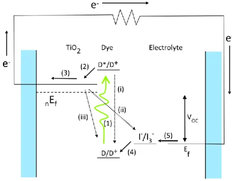
Figure 1.1 Process scheme of DSSC power generation. Forward (current and voltage contributing steps) are denoted by solid arrows and loss processes are denoted by dotted arrows. The forward processes area (1) excitation of dye by absorption of a photon, (2) electron injection in to conduction band of TiO2, (3) diffusion of injected electron through TiO2 film, (4) dye regeneration, and (5) reduction of oxidized redox species I3-. The loss processes are (i) dye relaxzation, (ii) electron recombination with
electrolyte, and (iii) electron recombination with oxidized dye. ... 3
Figure 1.2 Air mass 1.5 global tilt photon flux spectrum together with
cumulative photocurrent calculated from integrating the spectrum. ... 6
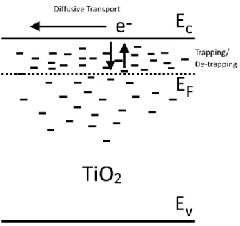
Figure 1.3 Diffusive transport within TiO2 mediated by trap states. ... 12
Figure 1.4 Equivalent circuit model of a DSSC with the electrical response of TiO2 modeled using a transmission line. Where RS is the series resistace of the cell, Rcon and Ccon are the contact resistance and capacitance between TiO2 and TCO, Rsub and Csub are the charge transfer resistance and double layer capacitance at the TCO/electrolyte interface, rtrans is the transport resistance in TiO2, cμ is the chemical capacitance of TiO2, rrec is the recombination resistance of charge transfer at the
TiO2/electrolyte interface, Zd is mass transport impedance of redox species in the electrolyte and RPt and CPt are the charge transfer resistance and double layer capacitance at the counter electrode TCO(Pt)/electrolyte
interface... 15
Figure 1.5 Nyquist plot of EIS spectra for the impedance of a complete
DSSC device and separate impedances for each component of a DSSC. ... 16
Figure 1.6 Water splitting photoelectrochemical cell using a single p-type semiconductor under illumination. The redox reactions occurring at the surface would be those occurring at higher pH as is used in our research. nEF is the electron quas-fermi leve, pEF is the hole quasi-fermi level, Ev is
the valence band edge and Ec is the conduction band edge. ... 18
Figure 1.7 Band bending of the conduction band EC for an n-type semiconductor cylinder in contact with a redox couple containing
electrolyte. R is the radius of the cylinder and r is the radial distance from the center of the cylinder to the beginning of the depletion layer. The ‘+’
symbols represent charges left in the depletion layer. ... 21
semiconductor/electrolyte interface. Note that if the nanostructure
developed a depletion region then the pathlength would be even shorter. ... 23
Fig. 2.1. Diagram of PLD system consisting of KrF laser, optical train
and deposition chamber. ... 29
Figure 2.2 ICCD pictures showing the plume evolution for a single laser shot over a range of background gas pressures. In these images the target is located on the right side of the frames while the substrate is located on
the left. ... 31
Figure 2.3 ICCD images showing temporal evolution of plume for pulse energies of 200 mJ and 300 mJ. These ablation were performed at the
same background gas pressure. ... 33
Fig. 2.4 SEM images of films deposited under various background pressures. The top row are imaged in profile view and the bottom row is
imaged looking down onto the top of the film. ... 34
Figure 2.5. A simple model of film growth based on particles undergoing a random walk with a velocity biased toward the ‘substrate’ (the bottom of the frame) The numbers indicate the amount of decrease in forward
momentum for each instance of the particle changing direction. ... 35
Figure 2.6. TEM images of isolated single nano-crystalline ITO trees formed at background pressures of (a) 100 mTorr, (b) 200 mTorr, (c) 300 mTorr and (d) 400 mTorr. Pictures to the right side of each panel are
magnified views of the trees. ... 37
Figure 3.1. Schematic image of fabrication process of patterned ITO on
FTO substrate. ... 47
Figure 3.2. SEM images of template of patterned hole (a), P-ITO on FTO substrate before removal of the template (b), P-ITO on FTO substrate
45-degree view (c), and cross-sectional view (d). ... 50
Figure 3.3. Absorbance of FTO (doted red line) and P-ITO (solid blue line) substrates, and FTO-Ta:TiO2 (doted green line), P-ITO-Ta:TiO2 (solid pink line), FTO-Ta:TiO2-Dye (doted purple line), and
P-ITO-Ta:TiO2-Dye (solid black line). ... 51
Figure 3.4. SEM images of Ta:TiO2 film on (a) FTO and (b) P-ITO substrates. Inset of (b) is a SEM image of Ta:TiO2 clearly deposited on
ITO spikes. ... 53
Figure 3.6. (a) Nyquist and (b) Bode plots from EIS, and (c) OCVD response for DSSCs with FTO (doted black line) and P-ITO (solid red
line) substrates. ... 57
Fig. 4.1 SEM images of films deposited under various background pressures. The top row are imaged in profile view and the bottom row is
imaged looking down onto the top of the film. ... 68
Fig 4.2 TEM images of isolated single nano-crystalline ITO branches formed at background pressures of (a) 100 mTorr, (b) 200 mTorr, (c) 300 mTorr and (d) 400 mTorr. Pictures to the right side of each panel are
magnified views of the branches... 69
Fig. 4.3. SEM images of ITO films (top view) deposited at (a) 200C and (b) room temperature under a background pressure of 300 mTorr (Ar/O2)
with all other parameters held constant. ... 70
Fig 4.4. SEM images comparing PLD ITO 200 mTorr deposited onto either FTO or smooth glass substrate. The top images are cross sectional views while the bottom images area looking down onto the tops of the
film. ... 70
Fig. 4.5. X-ray (Cu-α) diffraction spectra acquired of porous ITO films deposited under variable background chamber gas pressures. The main
In2O3 diffraction peaks are labeled. ... 71
Fig. 4.6 (a) Ru-C dye loading amounts and amount of dye found to be electroactive on PLD ITO films determined by the dye desorption method and cyclic voltammetry, respectively. (b) PLD ITO film densities
calculated from RBS measurements and specific dye loading amounts... 72
Fig 4.7. Rutherford backscattering spectra of PLD-ITO films from backscattered He nuclei collected at 160 degrees from incident path.
Model fits are overlaid onto raw spectra... 73
Fig. 4.8 Cyclic voltamagrams of Ru-C derivitized PLD-ITO films
deposited at varying pressures. ... 74
Fig 4.9. Sheet resistance values for PLD ITO films deposited onto glass
substrates derived from four point probe measurements. ... 75
Fig. 4.10. Pulsed laser (a)photovoltage and (b)photocurrent transients of DSSCS fabricated from N719 dyed PLD ITO/ALD TiO2 core/shell
photoanodes. Mono-exponential fits are overlayed. ... 77
Fig. 4.11 (a) SEM image of 200 mTorr PLD ITO coated with 50 cycle ALD TiO2 (b) TEM images show that the TiO2 is conformally coated
Fig. 4.12. Pulsed laser open circuit voltage transients (a)-(c) and short circuit current transients (d) for DSSCs made from PLD ITO 200 mTorr
films with ALD TiO2 conformal coatings of various thicknesses (cycles). ... 80
Fig. 4.13. Current density versus voltage curves of N719 derivatized 200 mTorr PLD-ITO films coated with ALD TiO2 conformal shells of
different thickness. Measurements were carried out in the dark and also
under an irradiance of 1 sun. ... 81
Figure 5.1 X-ray diffraction traces of (a) nanostructured (high pressure
deposited films) and (b) compact (low pressure deposited films). ... 95
Figure 5.2 Raman spectra acquired using an argon 514 nm wavelength
laser excitation source and confocal microscope. ... 96
Figure 5.3: Chemical potential domains in the planes of ΔμZn and ΔμZn illustrating conditions in which secondary phases are more stable than CZTS and the small narrow conditions under which CZTS is stable. These planes correspond to (a) Cu-rich conditions (ΔμCu= 0 eV) and (b)
Cu-poor conditions (ΔμCu= -0.41 eV) with sulfur vapor present. ... 97
Figure 5.4 UV-Vis spectra of CZTS films deposited at room temperature onto FTO substrates and subsequently sulfurized. Transmittance and reflectance (including scattering) spectra were acquired with the samples mounted at the entrance and exit window, respectively, of the integrating sphere. Absorptance was calculated using the reflectance and absorptance
values. ... 104
Figure 5.5 Current – Voltage curves for CZTS films in a 3-electrode cell configuration under chopped AM 1.5 light. The potential versus the Ag/AgCl (3M KCl) has been converted to the reversible hydrogen electrode RHE potential. All CZTS films were deposited on FTO except
LIST OF TABLES
Table 3.1. Device metrics of DSSCs with FTO and P-ITO substrates. ... 50
Table 4.1 Crystal sizes derived from the Scherrer equation using the full
width half maximum of the (222) plane peak for In2O3. ... 71
Table 4.2. Average lifetimes extracted from mono-exponential fits to pulsed laser open and short circuit transients of DSSCs fabricated from
N719 dyed porous PLD-ITO ITO with and without ALD –TiO2 shells. ... 77
Table 4.3 DSSC performance characteristics of N719 derivatized 200mTorr PLD-ITO films with different thicknesses of ALD TiO2
conformal shells. ... 81
CHAPTER 1: DYE SENSTIZED SOLAR CELLS AND PHOTOELECTROCHEMICAL WATER SPLITTING
1.1 The Need for Alternative Energy Technologies
The burning of fossil fuels has fueled the impressive industrial and technological growth
over the past roughly 150 years and allowed for the high standards of living much of the
developed nations enjoy. However, with more of the world’s population expected to achieve
higher living standards the demand on the limited fossil fuel reserves to supply the increased
power consumption will result in increased costs and negatively impact economic growth.
A more pressing concern is the CO2 released from burning fossils fuels contributing to
global warming. If left unchecked, global warming is expected to cause worldwide negative
impacts due to more extreme weather events, coastal flooding due to accelerated melting of the
icecaps and ocean acidification. Atmospheric concentration of CO2 has steadily increased since
the mid-20th century with a corresponding increase in the global average temperature. A record high 411 ppm of atmospheric CO2 was recently detected at the Mauna Loa Observatory in
Hawaii. Previous to the industrial revolution an average 300 ppm of CO2 was maintained for
hundreds of thousands of years. The Intergovernmental Panel on Climate Change holds to its
historical position that the most harmful effects can be prevented if warming is kept below 2 °C
by the year 2100 requiring CO2 emissions to be less than 450 ppm.
In order to prevent further rises in atmospheric concentrations of CO2 the world would
need to transition from burning fossil fuels to alternative energy technologies. Technologies
sunlight falls on the earth’s surface per hour than the world consumes in one year. Current costs
of commercially produced photovoltaics still need to be reduced to compete at a higher level in
the overall energy market. Dye sensitized solar cells are a cheaper potential alternative to current
commercially available solid state photovoltaics, but improvements in performance are required
to make them competitive. In addition, energy storage either in the form of batteries or
generation of fuels using the suns energy, directly or indirectly, will be required so that power
can be generated when the sun’s energy is not available such as at night or cloudy conditions.
The work in this dissertation involves both dye sensitized solar cells and the direct splitting of
water to produce hydrogen fuel are discussed further below.
1.2 Dye Sensitized Solar Cells
Dye sensitized solar cells (DSSCs) are regenerative photoelectrochemical cells which as
their name implies use a dye to absorb incident sunlight. The majority of research on DSSCs
have employed ruthenium complexes for the dye and I-/I3- for the redox couple. The dyes, typically ruthenium complexes, are chemi-adsorbed onto a porous wide band gap semiconductor
film, typically TiO2 and ~10μm thick, which is supported on top of a transparent conducting
oxide (TCO) and this composes the working electrode. The counter electrode consists of a thin
layer of platinum on TCO and is separated from the working electrode by ~ 50 μm . The cell is
filled with an electrolyte containing a redox couple like I-/I3-.
The power generation process in these devices is described as follows and shown in
Figure 1.1, where the solid arrows represent each step of the process. Photon absorption excites
an electron from the highest occupied molecular orbital (HOMO) to the lowest unoccupied
molecular orbital (LUMO) upon the absorption of a photon followed by injection of the excited
substrate then travels through the external circuit performing useful work. The dye now oxidized
is reduced by I- which through intermediate steps is converted to I3-, the oxidized form. This oxidized species diffuses a short distance, roughly 50 μm to the counter electrode where it is
reduced by electrons from the external circuit, forming a closed cycle.
Figure 1.1 Process scheme of DSSC power generation. Forward (current and voltage
contributing steps) are denoted by solid arrows and loss processes are denoted by dotted arrows.
The forward processes area (1) excitation of dye by absorption of a photon, (2) electron injection
in to conduction band of TiO2, (3) diffusion of injected electron through TiO2 film, (4) dye
regeneration, and (5) reduction of oxidized redox species I3-. The loss processes are (i) dye relaxation, (ii) electron recombination with electrolyte, and (iii) electron recombination with
oxidized dye.
only harvest a miniscule <1% of the incident sunlight leading to very poor solar conversion
efficiencies. After two decades of research and little improvement in efficiency a step-jump in
performance was achieved by Graetzel et. al.2 who employed a porous film composed of TiO2 nanocrystals which increased the surface area for dye loading by 1000-fold and led to impressive
efficiencies of 7-8%. Once it was realized that potentially competitive efficiencies could be
obtained by DSSCs the research in DSSCs increased dramatically in the ensuing decades. The
major commercial attractiveness of DSSCs is the low cost due to relative abundance and low
quality of TiO2 required as well as ease of fabrication along with the abundance of TiO2.
Additionally, unlike commercially available p/n junction solar cells where charge transport and
light absorption occur in the same material, in DSSCs these processes are decoupled. This
allows for greater flexibility in the quest for further improvement of efficiencies by optimization
of the sensitizer and oxide scaffolding separately.
The ultimate metric for evaluating the performance of any photovoltaic device is its power
conversion efficiency η. Electrical power generated by a power device is the voltage of the
device multiplied by the current J generated at that voltage V, P=J*V. The power conversion
efficiency is defined as the percentage of the incident solar power that is converted to electrical
power by the cell given by the equation
𝜂 =𝑃𝑚𝑎𝑥
𝑃𝑖𝑛 =
𝐹𝐹∗𝐽𝑆𝐶𝑉𝑂𝐶
𝑃𝑖𝑛 1.1
where Pmax is the maximum power output by the cell, Pinis the power of incident light, JSC is the
short circuit current density and VOC is the open circuit voltage. FF is the fill factor defined as
𝐹𝐹 =𝐽𝑚𝑎𝑥𝑉𝑚𝑎𝑥
where Jmax and Vmax and the current and voltage at the maximum power point. The FF gives an
indication of the device quality and primarily is affected by loss processes in the device which
will be discussed later. Therefore, both FF and JSC and VOC dictate the performance of the cell.
A widely adopted standard for measuring the efficiency of a PV cell is by illuminating
the cell using an artificial light source which is calibrated to match the photon flux distribution
hitting the earth’s surface when the sun is at an angle of 42° from the horizon, referred to as the
AM 1.5 spectrum, shown in Figure 1.2. This is commonly achieved using a Xenon light source
and AM 1.5 filter. The sun’s spectral irradiance resembles that of a thermal black body with a
temperature of approximately 5800 K. The power reaching the surface of the earth is modified
by the absorption of the atmosphere appearing as inverse peaks in the spectrum. The maximum
photocurrent which can be achieved by a photovoltaic device absorbing all photons with
wavelengths less than (energies greater than) the absorption threshold of the device is obtained
by integrating the AM 1.5 spectra up to the threshold wavelength and multiplying by the
elementary charge. This assumes that every photon incident of the solar device is converted to a
single charge. The maximum photocurrent is given in figure 2 as a function of wavelength. As
an example, the ruthenium complex designated N719, used in our research, has an absorption
onset around 780 nm which corresponds to a maximum possible photocurrent of ~26 mA cm-2. Taking into account actual losses using an assumption of 90% conversion efficiency of each
Figure 1.2 Air mass 1.5 global tilt photon flux spectrum together with cumulative photocurrent
calculated from integrating the spectrum.
Loss processes occurring within DSSCs prevent some fraction of incident photons from
contributing an electron to the photocurrent reducing the actual photocurrent obtained from
DSSCs. Some photons are reflected and absorbed by other components in the cell before
reaching the dye while some pass through the dye layer without being absorbed. For the
remaining photons which are absorbed, each forward process is countered by a reverse loss
process. The loss processes are indicated by dashed arrows in Figure 1.1. These loss processes
include dye relaxation after excitation and recombination with a component in the electrolyte or
oxidized dye after the electron has been injected into the conduction band of TiO2. The rates of
each forward process and the loss processes which oppose them dictate the efficiency of current
generation for each step. These are the injection efficiency φinj and the collection efficiency φcol
𝜑𝑖𝑛𝑗 = 𝑣𝑖𝑛𝑗
𝑣𝑖𝑛𝑗+𝑣0 1.3
𝜑𝑐𝑜𝑙 = 𝑣𝑡𝑟
where vinj is the rate of electron injection, v0 is the rate of electron relaxation, vtr is the rate of
electron transport and vrec is the rate of recombination with electrolyte. The rate of
recombination with the oxidized dye is not included due to the fact that the I- is usually present at a large concentration in the electrolyte and rapidly reduces the oxidized dye within a few
microseconds while electrons in the conduction band of titania TiO2(e-) recombine with the oxidized dye on the time scale of several hundred microseconds.3 Transport of TiO2(e-)s through the film occurs on the time scale of milliseconds the same order of magnitude as that of
recombination. Recombination with species in the electrolyte is therefore a more impactful loss
pathway since it occurs at a similar time scale as transport in the film. Typically, φinj is close to
unity since injection occurs on the timescale of femto- to pico-seconds and the luminescent
lifetime is typically nanoseconds.3 Additionally, light harvesting efficiency φLH accounts for the fraction of incident photons absorbed and is dependent upon the absorption coefficient of the dye
and electrolyte and transmittance of other components in the cell.
Collectively these efficiencies, which all may depend on the incident light wavelength λ,
determine what is termed the incident-photon-to-collected-electron efficiency (IPCE)
φIPCE(λ) = φLH(λ)φINJ(λ) φCOL(λ) 1.5
The IPCE is determined by illuminating the cell under monochromatic light and scanning over a
range of wavelengths while measuring the short circuit current jSC and power of the incident light
Pin. From this the IPCE is calculated using
𝜑𝐼𝑃𝐶𝐸 = 𝑗𝑆𝐶(𝜆)[𝐴 𝑐𝑚
−2]∗1240
𝑃𝑖𝑛(𝜆)[𝑊 𝑐𝑚−2] ∗𝜆[𝑛𝑚] 1.6
The total short circuit density of the cell can then be estimated by the overlap of φIPCE with the
spectral flux of the illumination source. For an AM 1.5 spectral source this would be
𝐽𝑆𝐶,𝐴𝑀 1.5 = ∫𝜆𝑚𝑎𝑥𝑞 ∗ 𝜙𝑖𝑛,𝐴𝑀 1.5∗ 𝜑𝐼𝑃𝐶𝐸𝑑𝜆
where λmin and λmax are the minimum and maximum wavelengths for the spectral output and
ϕin,AM 1.5 is the incident photon flux.
These loss processes also affect the open circuit photo voltage VOC of a DSSC. The VOC
is determined by the difference in fermi levels Ef at the two electrode contacts. The Ef of the
counter electrode is equivalent to the redox potential Eredox of the redox couple (I-/I3-) and the working electrode is approximately equivalent to the quasi-fermi energy of electrons nEf in TiO2,
see Figure 1.1. The concentration of electrons in the conduction band of a semiconductor nc is
related to nEf in the Boltzmann limit by
𝑛𝑐 = 𝑁𝐶𝑒𝑥𝑝 (−𝐸𝑐−𝑛𝐸𝐹
𝑘𝐵𝑇 ) 1.8
where NC is the effective density of states in the conduction band, EC is the conduction band
energy, kB is Boltzmann’s constant and T is the absolute temperature. In the dark nEf is at
equilibrium with Eredox and therefore
𝑛𝑐0 = 𝑁𝐶exp (−𝐸𝑐−𝐸𝑘𝑟𝑒𝑑𝑜𝑥
𝐵𝑇 ) 1.9
The photovoltage nEF-EF is then
𝑉𝑂𝐶 = 𝑘𝐵𝑇
𝑞 𝑙𝑛 𝑛𝑐
𝑛𝑐0 1.10
This explicitly shows that in order to maximize the VOC the concentration of conduction band
electrons must be maximized. Therefore, the loss processes must be minimized in order to build
up voltage within the cell.
The maximum VOC in DSSC can be manipulated by choice of the redox couple, dye and
semiconductor. A higher energy EC and lower Eredox result in a larger VOC. However the dye’s
lowest unoccupied molecular orbital LUMO and highest occupied molecular orbital HOMO
energetically favorable and drive the reaction. In N719/TiO2 systems, as used in our research,
the injection overpotential is approximately 300 mV while the overpotential for dye regeneration
using I-/I3- is larger at around 600 mV.4 A tradeoff in photovoltage and photocurrent generation occurs since increasing the energy gap between the HOMO and LUMO of the dye reduces that
fraction of the solar spectrum since only photons with energies larger than this energy difference
can be absorbed. DSSCs resemble a hetero p/n junction photovoltaic and the efficiencies
approach the 31% theoretical maximum as calculated by Shockley and Queisser3 for dyes
approaching the optimal band gap of 1.1 eV when losses are minimized.5 In our research the dye N719 and redox couple I-/I3- are used which has a maximum conversion efficiency of
approximately 13%.5
As discussed, the main loss pathway in DSSCs is recombination with the oxidized redox
species while the electron is transported through the TiO2 film to the TCO underneath. In solid
state p/n junction solar the transport is assisted by the presence of an electric field resulting from
the equilibration of fermi levels between the p- and n- doped layers. However, transport in
DSSCS occurs through diffusion. The small size < 20 nm size particles of TiO2 in DSSCs and
the large difference of fermi level in the TiO2 and that of the redox couple results in complete
depletion of the mobile charges in TiO2 leaving only positive defects within the nanocrystal. The
amount of band bending in a spherical particle can be calculated using Poisson’s equation which
results in the voltage difference between the outer interface and center of the particle
∆𝑉 =𝑞𝑁𝐿𝑟2
6𝜀0𝜀𝑟 1.11
where NL is the defect density, r is the particle radius, and εr is the dielectric constant. Using a
bending of approximately 4 meV which is less than the thermal energy the electron possesses at
room temperature of ≅25 meV.
Lacking a large electric field to drive the TiO2(e-)s to the back contact they travel
diffusely through the film. The dynamics of the conduction band electrons nc are modeled by the
continuity equation
𝜕𝑛𝑐
𝜕𝑡 = 𝐺 + 𝐷0 𝜕2𝑛𝑐
𝜕𝑥2 −
𝑛𝑐−𝑛0
𝜏0 1.12
where
𝐺 = 𝜂𝑖𝑛𝑗𝛼𝐼0exp (−𝛼𝑥) 1.13
and ηinj is the injection efficiency of electrons from the dye into the oxide, I0 is the incident light
intensity and α is the absorption coefficient of the dye, D0 is the diffusion coefficient of
conduction band electrons and τ0 is the electron lifetime. The first term on the right is charge
generation by photon induced charge injection, the second term describes diffusion of the
charges and the remain term accounts for the loss of electrons due to recombination. In this case
the rate of recombination is pseudo-first order vrec=krecnc and krec=1/τ0.
The continuity equation was solved by Södergan6 for steady state conditions (dnc/dt=0) and the solution takes the form of the diode equation
𝑗 = 𝑗𝑝ℎ− 𝑗0(𝑒𝑥𝑝𝑒𝑉𝑘𝑇− 1) 1.14
where
𝑗𝑝ℎ = 𝑞𝜑𝑖𝑛𝑗𝐼0(1 − exp(−𝛼𝑑)) 1.15
𝑗0 =𝑞𝐷0𝑛𝑐
0𝑑
𝐿02 =
𝑒𝑛𝑐0𝑑
𝜏0 1.16
where L0=(D0τ0)1/2 is the average diffusion length for electrons in the conduction band and d is
increasing L0. Assuming D0 is fixed by the material then τ0 should be maximized. L0 can be
related to related to the collection efficiency.7 A high collection efficiency >90% requires L0/d ratios that are greater than 2.8
Given the importance of lifetime and diffusion several techniques have been developed to
measure them. One method of determining these constants involves perturbing the system by
injecting a small amount of charge into the device either through illumination or voltage and
monitoring the relaxation of this charge back to steady state. When performed at open circuit the
voltage is monitored while in short circuit conditions the current is monitored. The small signals
can be either sinusoidally varying light signals as used in intensity modulated photocurrent
spectroscopy IMPS and intensity modulated photovoltage spectroscopy IMVS or small light
pulses as used transient photocurrent TPC and transient photovoltage TPV techniques. TPV and
IMVS are performed at open circuit which prevents transport and therefore the signal relaxation
is only due to recombination processes and therefore allows for τn to be determined. Under the
short circuit conditions of TPC and IMPS the charges are transported out of the cell and these
techniques also allow for Dn to be determined. In addition to these techniques electrical
impedance spectroscopy EIS has also become a popular measurement technique. In this
technique a small periodic voltage is applied to the device and the current response is measured
as the frequency of the periodic voltage is scanned over a wide range of frequencies.
Researchers discovered that the small perturbation time constants derived from these
techniques depend on the operating condition of the cell. Since these constants depend on the
operating conditions (position of the quasi fermi level) they are referred to as effective values
and denoted by Dn and τn. A widely adopted framework to explain this effect is based upon the
lower energy trap state and released thermally back to the conduction band, see Figure 1.3. The
degree of trapping/detrapping depends on the occupancy of the traps states which is represented
by the quasi-fermi energy. Charge extraction techniques where-in photocurrents are integrated
after short circuiting a cell which had been held at open circuit irradiated by set light intensities
found an exponential distribution of the traps.9 The occupation of the traps also follow Boltzmann statistics and the density of electrons occupying localized trap states is
𝑛𝐿= 𝑁𝐿𝑒𝑥𝑝 (𝛽𝐸𝐹−𝐸𝑐
𝑘𝐵𝑇 ) 1.17
Where NL is the total density of localized trap states and β=T/T0 where T0 is the characteristic
temperature of the trap state distribution. T0 affects the width (slope) of the trap state
distribution and is found to be 600 – 1500 K.9
Many researchers have adopted the multiple trapping framework developed by Bisquert
and Vikhrenko.10 to elucidate the effects trap mediated recombination and transport. In this model only the free electrons in the conduction band contribute to the diffusion current. It is
assumed that a quasi-static (dynamic) equilibrium exists between the free conduction band
electrons nc and those populating localized trap states nL , represented as:
𝜕𝑛𝑐 𝜕𝑡 = 𝜕𝑛𝑐 𝜕𝑛𝐿 𝜕𝑛𝐿 𝜕𝑡 1.18
The relationship between the free electron D0 and τ0 to the small amplitude Dn and τn are
predicted by this model to be
𝜏𝑛 = (1 +𝜕𝑛𝐿
𝜕𝑛𝑐) 𝜏0 1.19
𝐷𝑛 = (1 +𝜕𝑛𝜕𝑛𝐿
𝑐)
−1
𝐷0 1.20
The dependency of the constants τn and Dn on light intensity is explained by the term ∂nL/∂nc
which is related to the exponential trap state distribution by
𝜕𝑛𝐿
𝜕𝑛𝑐=
𝜕𝑛𝐿
𝜕𝑛𝐸𝐹
𝜕𝑛𝐸𝐹
𝜕𝑛𝑐 = 𝑔( 𝐸𝐹)
𝑘𝐵𝑇
𝑛𝑐
𝑛 1.21
And g(nEF) is the exponential density of trap state distribution
𝑔(𝐸) =𝑁𝐿𝛽
𝑘𝐵𝑇exp (𝛽
𝐸−𝐸𝑐
𝑘𝐵𝑇) 1.22
The dynamic trapping and detrapping of the electrons results in larger effective electron
lifetimes and smaller effective diffusion coefficients. Increasing light intensity (larger nEF)
attenuates the effect of the trap states and therefore τn decreases while Dn increases such that the
product Dnτn stays the same. The average diffusion length L of the electrons is given by
𝐿 = √𝐷𝑛𝜏𝑛 = √𝐷0𝜏0 1.23
electrons in the film and D0 and τ0 are independent of electron concentration. The independence
of electron diffusion length on light intensity has been demonstrated by Peter et. al. using IMVS
and IMPS techniques.11
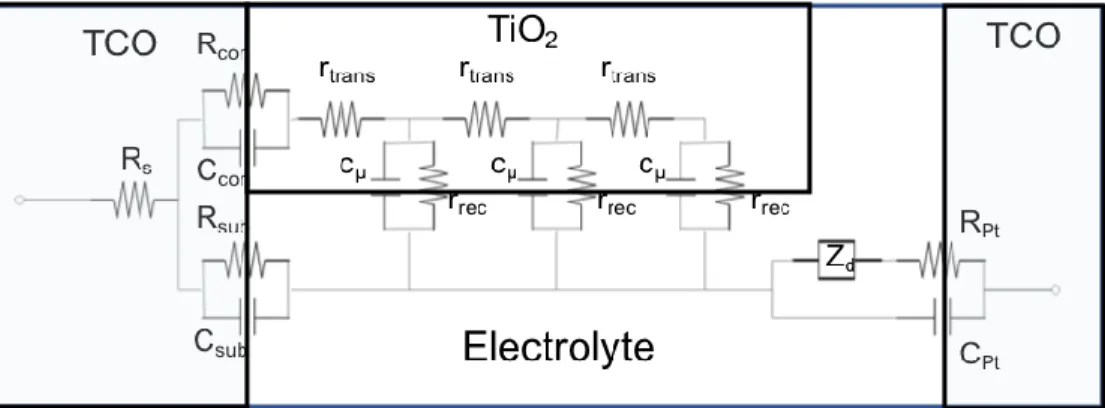
As mentioned, EIS is carried out by applying a small 5-10 mV periodic voltage to the
device ranging from 10-100kHz to 1 mHz and measuring the current and its phase. In order to
interpret the results, the DSSC must be modeled as a network of circuit elements corresponding
to charge transport and accumulation within and between phases of the device. Two different
models describing the impedance measurements of DSSCs were developed Kern12 and
Bisquert13. The equivalence of the two models was worked out by Adachi et. al.14 and we will therefore discuss EIS of DSSCs using Bisquert’s13 analysis. The equivalent circuit of a DSSC is
shown in Figure 1.4 . The major feature of this model is the transmission line which represents
the diffusion of electrons in the TiO2 along with their recombination with redox species in the
electrolyte. Parallel to the transmission line is the impedance element Zd which accounts for the
diffusion of redox species in the electrolyte carrying the positive charge to the electrolyte. The
various interfaces in the cell are represented with parallel resistor and capacitor accounting the
charge transfer resistances and charge build-up at the interface. It is usually necessary to use
Figure 1.4 Equivalent circuit model of a DSSC with the electrical response of TiO2 modeled
using a transmission line. Where RS is the series resistace of the cell, Rcon and Ccon are the
contact resistance and capacitance between TiO2 and TCO, Rsub and Csub are the charge transfer
resistance and double layer capacitance at the TCO/electrolyte interface, rtrans is the transport
resistance in TiO2, cμ is the chemical capacitance of TiO2, rrec is the recombination resistance of
charge transfer at the TiO2/electrolyte interface, Zd is mass transport impedance of redox species
in the electrolyte and RPt and CPt are the charge transfer resistance and double layer capacitance
at the counter electrode TCO(Pt)/electrolyte interface.
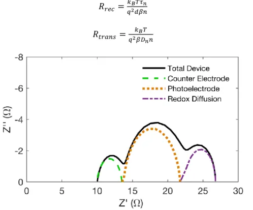
The imaginary part of the impedance can be plotted against the real impedance in what is
known as a Nyquist plot. A model Nyquist plot using the circuit in Figure is shown in Figure
1.5. Generally, three arcs are observed corresponding from high to low frequency to impedance
originating from the platinum counter electrode interface, diffusion and recombination of charge
in the oxide film and diffusion of redox species in the electrolyte. Depending on the time
constants of these processes and the steady state voltage of the cell the three arcs may not be
distinguishable. Fitting the model provides values for important properties of the photoelectrode
including charge recombination resistance rrec, charge transport resistance rtrans, and the chemical
𝑅𝑟𝑒𝑐 =𝑟𝑟𝑒𝑐
𝑑 1.24
𝑅𝑡𝑟𝑎𝑛𝑠= 𝑟𝑡𝑟𝑎𝑛𝑠𝑑 1.25
𝐶𝜇 = 𝑐𝜇𝑑 1.26
where d is the film thickness. These macroscopic parameters and related to the small
perturbation parameters τn and Dn by
𝑅𝑟𝑒𝑐 =𝑘𝐵𝑇𝜏𝑛
𝑞2𝑑𝛽𝑛 1.27
𝑅𝑡𝑟𝑎𝑛𝑠 =𝑞2𝑘𝛽𝐷𝐵𝑇𝑛𝑛 1.28
Figure 1.5 Nyquist plot of EIS spectra for the impedance of a complete DSSC device and
separate impedances for each component of a DSSC.
1.3 Photoelectrochemical Water Splitting
The intermittency of solar photovoltaic power production requires the development of
efficient means to store energy periods when power output ceases such as during the night and
some stored form of energy can be used. One way of storing energy is through chemical means
used for power generation. One highly researched means to do this is by photoelectrochemically
splitting water and forming high energy bonds in H2 and O2 given by the reaction:
𝐻2𝑂 →12𝑂2 + 𝐻2 1.29
The Gibbs free energy change of the reaction is +237.2 kJ/mol and in the context of
electrochemistry a voltage of 1.23 V. In a basic electrolyte (used in this research) the overall
reaction in an electrochemical cell is composed of the following two reactions occurring at the
cathode and anode
4𝑂𝐻− → 𝑂
2+ 2𝐻2𝑂 + 4𝑒− (𝑉𝑎𝑛𝑜𝑑𝑒= 1.23 𝑉 𝑣𝑠 𝑅𝐻𝐸) 1.30
4𝐻2𝑂 + 4𝑒−→ 2𝐻
2+ 4𝑂𝐻−(𝑉𝑐𝑎𝑡ℎ𝑜𝑑𝑒 = 0.0 𝑉 𝑣𝑠 𝑅𝐻𝐸) 1.31 Note that RHE stands for reversible hydrogen electrode and takes into account the ~60 mV
change in hydrogen electrode potential per pH unit calculated using the pH of the electrolyte
used for testing. The redox potential values above correspond to pH 14. One of the simplest
ways to carry out these reactions is to use the energy of electron-hole pairs generated in
semiconductors by the absorption of sunlight to drive the reactions at the surface, see Figure 1.6
If a single semiconductor is used it is thermodynamically necessary that the quasi-fermi
levels of the electrons and holes in the semiconductor under illumination straddle the OH-/O2 and H2O/H2 redox potentials. In real devices overpotentials are required for adequate currents so that
the difference in quasi-fermi levels, the photovoltage of the device, should be from 1.6 – 2.4 V to
Figure 1.6 Water splitting photoelectrochemical cell using a single p-type semiconductor under
illumination. The redox reactions occurring at the surface would be those occurring at higher pH
as is used in our research. nEF is the electron quas-fermi level, pEF is the hole quasi-fermi level,
Ev is the valence band edge and Ec is the conduction band edge.
The maximum theoretical efficiencies water splitting using a single semiconductor are
calculated similar to those of photovoltaic devices. The assumptions being that all photons with
energies above the bandgap are absorbed and the only radiative recombination occurs. However,
in the case of photoelectrolysis only part of the energy of the electron hole pair, roughly ¾ of the
band gap energy, can be used to generate the product due to entropic losses.21 Therefore the minimum band gap is roughly 2.2 eV. The efficiency is calculated as
𝜂 =𝐽𝑔𝜇𝑒𝑥𝜙𝑐𝑜𝑛𝑣
𝑆 1.32
where Jg is the absorbed photon flux, μex is the excess chemical potential, ϕconv is the quantum
yield for conversion of absorbed photons to products. Under irradiation by the AM 1.5 solar
spectrum, the ideal theroretical efficiency of a single semiconductor system requiring two
However, in a real device other losses such as overpotential losses are encountered. A more
realistic loss of 0.8 eV limits the efficiency to 17% corresponding to a band gap of ~ 2 eV. In
general, the greater the losses the larger the band gap required which reduces amount of photon
absorption.
1.4 Nanostructured Electrodes Use of Nanostructures in DSSCs:
The use of porous films greatly increased the efficiency of DSSCs as more light was
harvested and converted into photocurrent due to the larger surface area. Building upon the
benefits realized by nanoparticle films researchers have investigated other nanostructured porous
film morphologies in an attempt to further improve device performance15–22. These structures include nanowire20–22 and nanotubes16,18 grown perpendicular to the substrate. Nanotubes are typically formed through anodization of metal foils or thin films while rods (wires) are grown
hydrothermally.
The primarily motivation behind using these nanostructures is the potential improvement
in collection of photogenerated charge. One method for improving charge collection is by
providing the injected electron a more direct route to the substrate. The diffusion mechanism of
charge transport in nanocrystalline films involves a random walk of the charges which meanders
both laterally as well as toward the substrate. Restricting the lateral available path to within the
confines of the nanotubes(wires) directs the charge to the substrate, potentially decreasing the
residence time within the film. This would decrease the chance for recombination.
A further decrease in charge loss due to recombination may be achieved if the wire is not
fully depleted and band bending only occurs at the circumference of the wire as shown in Figure
surface of the wire where recombination with the electrolyte could occur by the electric field set
up in the depletion region around the circumference of the wire. In addition, the center of the
wire would not be depleted and therefore the conductivity is higher than in the fully depleted
(highly resistant) interiors of the nanocrystalline film. Therefore, the wire would act like a
conduit for the charges. The voltage drop across the depletion layer in a wire (cylinder) is
related to the doping density ND and radius of the wire R by
𝑉𝑆𝐶 = 𝑞𝑁𝐷
2𝜀0𝜀𝑟(
1 2(𝑟
2− 𝑅2) + 𝑟2𝑙𝑛 (𝑅
𝑟)) 1.33
where r is the inner boundary of the space charge region. At equilibrium in the dark the band in
TiO2in equilibrium with a I-/I-3 redox system will be roughly 1 eV. Using the same values for TiO2 as above, εr=100 and ND=1017 cm-3, under these condition nanowires less than
approximately 470 nm in radius will be fully depleted. The voltage drop at the device operating
point will be less and therefore the depletion width reduced leaving the center of the wires
undepleted possessing higher conductivity. These dimensions are rather large and would
significantly reduce the surface area of the electrode reducing the maximum achievable
photocurrent. If the TiO2 were more highly doped, say 1018 cm-3 full depletion would occur for < 150 nm radius wires in the dark. Therefore, higher doping would be required to obtain the
Figure 1.7 Band bending of the conduction band EC for an n-type semiconductor cylinder in
contact with a redox couple containing electrolyte. R is the radius of the cylinder and r is the
radial distance from the center of the cylinder to the beginning of the depletion layer. The ‘+’
symbols represent charges left in the depletion layer.
Collection efficiencies for photoinjected charges of close to 100% for 20 μm TiO2
nanotubes were reported by Jennings et. al.16 This demonstrates the enhanced capability of 1-D nanostructures to achieve a large reduction in recombination, but also highlights the loss in
surface area which reduced the photocurrent and produced an efficiency of only 2.61%.16 Similar observations have been made using nanowires. Matt et. al.22 grew vertically aligned single crystalline ZnO nanowires with estimated diffusion coefficients hundreds of times larger
than those of nanoparticle films, but the roughness factor (total surface area of electrode /
geometric area) of the nanowire electrode was only 1/5 that of nanoparticulate films. In part due
to the reduced surface area in spite of charge collection efficiencies the nanowire devices
wires by the concurrent lateral growth of the wires. Higher efficiencies were seen with 2 μm
thick films than in thicker films; however the superiority in charge collection efficiency over
nanoparticle films was exhibited by their efficiency being the same as 5 μm thick films.20
Use of Nanostructures in Photoelectrochemical Cells:
The situation is slightly different when using nanostructured semiconductors for water
splitting. As discussed previously, maximizing the flux of minority carriers and their build up at
the surface is desired for high rates of product formation. As mentioned the rate of electron hole
pair generation is increased by lengthening of the light pathlength through scattering and
reducing the amount of light lost to reflection. Another major benefit frequently touted is the
reduced path length for minority carriers from their generation to the semiconductor interface.
The Gartner equation23 is usually referenced to describe this benefit. The normalized form of it relates the EQE to the space charge layer width Wsc
𝐸𝑄𝐸 = 1 −1+𝛼𝐿𝑒−𝛼𝑊𝑆𝐶
𝑚𝑖𝑛 1.34
where α is the absorption coefficient. This equation is based conceptually on the idea that if the
minority carrier is generated at a distance further than Lmin from the depletion layer then the
minority carrier will most likely recombine before reaching depletion layer as shown in Figure
1.8. In the figure 1/α is used as the penetration depth of light which is the depth at which light
has been attenuated to 1/e of its original value. Light is reduced by 90% at depth of 2.3 times 1/α
which can be in the micron range for direct band photon absorption. The absorbing layer should
then be comparable in thickness to absorb as much of the incident light as possible. However,
many materials used for water splitting have Lmin values of only tens of nanometers and therefore
electrode can ensure that minority carriers are generated close to an interface no matter the depth
at which they are generated within the film.
Figure 1.8 Photogenerated charge generation and transport in bulk and nanostructured
semiconductors. The diffusion length of the minority carrier is too short for the carrier to reach
the depletion region in the bulk semiconductor, but the pathlength is shortened in the
nanostructured semiconductor on the right allowing the carrier to reach the
semiconductor/electrolyte interface. Note that if the nanostructure developed a depletion region
then the pathlength would be even shorter.
In the derivation of the Gartner equation it is assumed that no recombination occurs in the
space charge region. However, Peter et. al. has argued that recombination often does occur in
the space charge region which appears to be a major source of minority carrier loss in the case of
of hematite.24 It should be noted too that this model does not apply to nanostructures that have low doping concentration (<107 cm-3) and as a result are fully depleted and band bending is minimal. However, the shorter path lengths should still reduce the amount of minority carrier
recombination since in the depleted region even with a small electric field the majority carrier
Nanostructuring can also have negative impacts on the performance of PECs. The
greater surface area may allow for smaller overpotentials since there is greater surface area for
reactions to occur, but the larger surface area may also enhance recombination of majority
carriers with species in the electrolyte. This would be exacerbated in low doped semiconductors
by a reduced barrier due to smaller band bending which again is more likely in nanostructured
electrodes. The larger surface area also dilutes the flux of the minority carriers which is related
to the VOCby the diode equation
𝑉𝑂𝐶 =𝑘𝐵𝑇
𝑞 𝑙𝑛 ( 𝐽𝑆𝐶
𝛾𝐽0) 1.35
where JSC is the short circuit density, J0 is saturation current density and γ is the total junction
area of the electrode per unit geometrical area. The VOC is a measure of the quasi-fermi level
splitting and therefore the driving force for water reduction/oxidation. Assuming JSC >> J0 a
decrease of ~60 mV per factor of 10 increase in the junction area is expected. Increased photon
harvesting due to light scattering should offset this to some extent. In addition, the use of a
catalyst could also decrease the need for large overpotentials to drive the reaction.
Therefore, it’s difficult to predict if nano-structuring will ultimately be beneficial for any
given material. However, nano-structuring has led to efficiency improvements of several
materials. Notably, substantial current densities of up to 3 mA cm-2 at 1.23 VRHE have been achieved for hematite electrodes in spite of very low minority diffusion lengths of 2-4 nm.25
In our research the effects of nano-structuring Cu2ZnSnS4 CZTS by depositing using
PLD at relatively high chamber pressures on its performance as a photocathode for the hydrogen
evolution reaction is investigated. CZTS is a p-type semiconductor with a band gap of ~1.5 eV
configuration.27 The absorption coefficient is on the order of 104 cm-1 so that penetration depths are around 600 to 700 nm.28 Minority carrier diffusion lengths in high quality films are reported to be around 350 nm.29 Therefore some improvement may be achieved by shortening the
minority carrier pathlength to the interface by nano-structuring. Some demonstrations of
enhanced performance as a result of nanostructuring via other synthesis methods have recently
been demonstrated and the application of this morphology paradigm remains of great importance
REFERENCES 1. Osa, T.; Masamichi, F. Nature 1976, 264, 349-350.
2. O’Regan, B.; Grätzel, M. Nature 1991, 353, 737–740.
3. Hagfeldt, A.; Boschloo, G.; Sun, L.; Kloo, L.; Pettersson, H. Chem. Rev. 2010, 110, 6595-6663.
4. Hardin, B. E.; Snaith, H. J.; McGehee, M. D. Nat. Photonics 2012, 6, 162-169.
5. Snaith, H. J.; Adv. Funct. Mater. 2010, 20, 13–19.
6. Soedergren, S.; Hagfeldt, A.; Olsson, J.; Lindquist, S.; J. Phys. Chem. 1994, 98, 5552-5556.
7. Barnes, P. R.; Miettunen, K.; Li, X.; Anderson, A. Y.; Bessho, T.; Gratzel, M.; O’Regan, B. Adv. Mater. 2013, 25, 1881–1922.
8. Peter, L. Acc. Chem. Res. 2009 42, 1839–1847.
9. Bailes, M.; Cameron, P.; Lobato, K.; Peter, L. J. Phys. Chem. B 2005, 109, 15429–15435.
10. Bisquert, J.; Vikhrenko, V. S. J. Phys. Chem. B 2004, 108, 2313–2322.
11. Peter, L. M.; Wijayantha, K. G. U. Electrochem. Commun. 1999, 1, 576–580.
12. Kern, R.; Sastrawan, R.; Ferber, J.; Stangl, R.; Luther, J. Electrochim. Acta 2002, 47, 4213-4225.
13. Bisquert, J. J. Phys. Chem B 2002 106, 325–333.
14. Adachi, M.; Sakamoto, M.; Jiu, J.; Ogata, Y.; Isoda, S. J. Phys. Chem. B 2006 110, 13872– 13880.
15. Meekins, B. H.; Kamat, P. V. ACS Nano 2009 3, 3437–3446.
16. Jennings, J. R.; Ghicov, A.; Peter, L. M.; Schmuki, P.; Walker, A. B. J. Am. Chem. Soc. 2008, 130, 13364–13372.
17. Tena-Zaera, R.; Elias, J.; Levy-Clement, C.; Bekeny, C.; Voss, T.; Mora-Sero, I.; Bisquert, J. J. Phys. Chem C. 2008, 112, 16318–16323.
19. Mora-Seró, I.; Fabregat-Santiago, F.; Denier, B.; Bisquert, J.; Tena-Zera, R.; Elias, J.; Levy-Clement, C. Appl. Phys. Lett. 2006, 89, 203117_1-203117_3.
20. Feng, X.; Shanker, K.; Varghese, O. K.; Paulose, M.; Latempa, T. J., Grimes, C.A. 2008 Nano Lett. 2008, 8, 3781–3786.
21. Tornow, J.; Ellmer, K.; Szarko, J.; Schwarzburg, K. Thin Solid Films 2008, 516, 7139–7143.
22. Law, M.; Greene, L. E.; Johnson, J. C.; Saykally, R; Yang, P. Nat. Mater. 2005, 4, 455-459.
23. Gärtner, W. W. Phys. Rev. 1959, 116, 84–87.
24. Peter, L. M.; Gurudayal, Wong, L.; Abdi, F. F. J. Electroanal. Chem. 2018, 819, 447-458.
25. Sivula, K.; Le Formal, F.; Grätzel, Chemsuschem 2011 4, 432–449.
26. Wang, J.; Yu, N.; Zhang, Y.; Zhu, Y.; Fu, L.; Zhang, P.; Gao, L.; Wu, Y. J. Alloys Compd 2016 688, 923–932.
27. Jiang, F.; Gunawen, Harada, T.; Kuang, Y.; Minegishi, T.; Domen, K.; Ikeda, S. J. Am. Chem. Soc. 2015, 137, 13691–7.
28. Katagiri, H.; Jimbo, K.; Maw, W.; Oishi, K.; Yamazaki, M.; Araki, H.; Takeuchi, A. Thin Solid Films. 2009, 517, 2455-2460.
29. Shin, B.; Zhu, Y.; Bojarczuk, N.; Chey, S. J.; Guha, S.; Prog. Photovoltaics Res. Appl. 2013, 21, 72-76.
30. Sarswat, P. K.; Deka, N.; Rao, J. S.; Free, M. L.; Kumar, G. J. Electron. Mater. 2017, 46, 5308–5318.
CHAPTER 2: PULSED LASER DEPOSITION OF NANOSTRUCTURED FILMS AND UTILIZATION IN PHOTOELECTROCHEMICAL CELLS
Pulsed laser deposition (PLD) is in practice a relatively simple and straight forward
vacuum technique using the energy of a laser to evaporate a small surface layer of material
which is deposited onto a substrate. The first demonstration of thin film deposition using a high
powered laser dates back to 1965 when Smith and Turner used a ruby laser to deposit thin films
froma variety of materials.1 Although showing promise for the deposition of thin films, including semiconductors, research into PLD of thin films remained muted until Dijkkamp et.
al.2 demonstrated the successful growth of high quality high-temperature YBCO
superconducting thin films by PLD. This demonstration along with improvements in laser
design and reduction in their costs has led to a substantial increase in PLD research in the past
several decades.
The near stoichiometric transfer of even complex materials like YBCO from target to
film is a major attraction of the PLD technique. This is primarily due to the rapid heating and
vaporization of the surface layer of the film limiting subsurface melting and incongruent thermal
evaporation. High powered pulsed lasers producing energies from 1-10 J/cm2 with pulse widths in the low 10s of nanoseconds are typically used for PLD of thin films. UV wavelengths are
primarily used since light absorption in materials generally increases the shorter the light
wavelength thus shortening the penetration depth and transferring the bulk the incident laser
medium, have become a popular choice in the PLD research community due to their ability to
obtain high pulse rates in the hundreds of hertz with pulse energies up to 500 mJ/pulse.3 We use an excimer laser with a KrF gas emitting 248 nm wavelength light for the
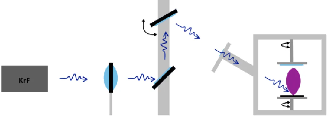
deposition of all of our thin films produced in this research. A schematic of our PLD setup is
shown in Figure 2.1. The optical path consists simply of two mirrors and a lens. The first
element in the path is a focusing lens followed by a mirror set to a 45 degrees which reflects the
horizontal laser beam vertically to a second mirror set to an angle of 30 degrees. After reflecting
from the 2nd mirror the laser beam passes through the entrance window of the chamber and impinges on the target generating an ablation plume traveling vertically to the substrate. The 2nd mirror is a 3 point mounted mirror with a motorized actuator that allows the beam to be rastered
across the surface of the target. Gas can be introduced into the chamber through two flow
controllers allowing either two gasses to be simultaneously or just one. A turbo pump is used to
draw an ultrahigh base vacuum (up to 1x10⁻⁶ Torr) while a VAT controller allows for control of chamber pressure once the background gas has been introduced.
Fig. 2.1. Diagram of PLD system consisting of KrF laser, optical train and deposition chamber.
PLD as shown in the schematic above is a conceptually simple deposition technique,
plume to be recorded using a gated intensified charge couple device ICCD as seen in Figure 2.2.
From these TOF recordings researchers have found that both a classical or modified
hydrodynamical drag model4,7 and a blast wave model4 adequately describe the trajectory of the plume. These models apply only to the plume evolution after cessation of the laser pulse and
initial plume formation. A summary of plume evolution follows.
The large amount of energy involved in the evaporation results in a partially ionized
plasma plume and these ions are accelerated by laser-ion interactions up to velocities > 106 cm/s corresponding to kinetic energies >50 eV (depending on atomic mass) and resulting in a highly
forward biased velocity distribution.3,4,6 The rapidly expanding plume of ions, neutral atoms and molecules plow into background gas atoms pushing them back and developing a shockwave at
the lead edge of the plume resulting in the bowing seen in the early times of the ICCD images
shown in Figure 2.2. When pressures are kept low enough the stopping distance of this plume
can be dozens of centimeters beyond the substrate and much of the plume material reaches the
substrate within 10 μs as highly energy ions, atoms and small molecules favorable for forming
compact films. At higher pressures the collisions at the boundary are enhanced and momentum
is bled from the plume at a faster rate to an extent that at higher pressures the visible plume is
stopped before reaching the substrate and hovers in between the substrate and target. It’s
interesting to note that at pressures slightly lower than those which halt the plume completely,
the plume can rebound off the substrate and target then come to rest in the space between.7 Light emission continues for hundreds of microseconds until gradually dying off as the plume
Figure 2.2 ICCD pictures showing the plume evolution for a single laser shot over a range of
background gas pressures. In these images the target is located on the right side of the frames
while the substrate is located on the left.
The containment of the plume at higher pressures and the associated increase in
scattering leads to significant generation of molecular species and eventual formation of
nanoclusters within the film. Geohegan et. al.8 tracked both of these species during the deposition of YBCO in an oxygen background using laser induced fluorescence to detect the
molecular oxide species and Rayleigh scattering of the laser light to detect the formation of
nanoparticles. During the initial plume expansion, the molecular species travels just ahead of the
emissive plasma while scattering mixes the molecular species within the full plume volume at
the later diffusive stage of the plume. The fluorescence signal from the molecular oxide species
rapidly decays and disappears after 3 ms while Raleigh scattering from the nucleating
several 100 ms and persist as a diffusive cloud hovering between the target and substrate for up
to several seconds.8
The gas phase nanocluster formation at higher pressures seems to be a general
phenomenon occurring for a variety of materials including SnO29, TiO210–18,25 , WO310, ZnO17, Mn3O418, Pt19, Sm0.2Ce0.8O1.9-δ20 and Nb2O524. Nanocluster formation will occur within inert background gasses like argon and helium as well as reactive background gasses like oxygen.
Plume confinement is the primary factor which dictates the gas phase formation of nanoparticles
requiring sufficient background gas pressures to obtain scattering rates sufficient for substantial
loss of kinetic energy to halt the plume between the target and substrate. The pressure threshold
above which gas phase nanocluster formation occurs depends on the relative masses of the
ablated atoms and background gas atoms/molecules.5 A lower pressure is adequate for nanoparticle formation when more massive background gas atoms/molecules are used since a
greater loss in the ablated atom’s momentum occurs in collisions with the heavier background
gas. Additionally, the laser power is an important parameter since a larger laser pulse power
accelerates the plume species to higher velocities requiring more collisions to slow the particles
achieved through use of higher background pressures. Figure 2.3 demonstrates this as the plume
generated with the larger laser power travels faster and reaches a stopping point at a further
distance from the target than the plume generated at lower laser power at the same background
Figure 2.3 ICCD images showing temporal evolution of plume for pulse energies of 200 mJ and
300 mJ. These ablation were performed at the same background gas pressure.
The transition into the nanocluster formation regime is reflected in the thin film
appearance evolving from compact films at low pressure to nanostructured bushes composed of
the gas phase particles as seen in Figure 2.4. The threshold pressure at which noticeably bushy
structures start to appear correspond to the visible plume stopping just before reaching the
substrate. Higher pressures will halt the visible plume at distances increasingly further from the
substrate. Nanoparticles which form in the plume diffuse outward in all directions and can travel
several centimeters from the edge of the visible plume.7 The nanoparticles generated under these conditions are amorphous and have dimensions anywhere from 2 nm to 20 nm.
Once reaching the substrate the randomly colliding nanoparticles will also collide with
the substrate and some will ‘stick’ if their kinetic energy is low enough others will rebound and
continue undergoing collisions within the cloud. A former member of our group modeled these
nanoparticle dynamics and film growth using a modified diffusion limited approach. In the
biased motion toward the substrate. The particles undergo a random walk with each change in
direction factored as an impact through a small decrement in forward momentum. In the model
the particles would “stick” to the film if the particle’s velocity was below a certain value. The
effect of pressure was taken into account by using a larger decrement of forward momentum for
higher background pressures. This effect can be seen in Figure 1.5 with smaller decrements
leading to a compact film while higher decrements led to the bushy hierarchically structured
forms as seen in the SEM pictures of Figure 2.4. The more random the motion of the particles
(the less forward biased) the more porous and fluffy in appearance the structures become. This
is due to the increasing probability that particles will collide with the highest part of the
structures before traveling into the film.
Fig. 2.4 SEM images of films deposited under various background pressures. The top row is a
crosssection view and the bottom row is a view looking down onto the top of the films.
20 mTorr
50 mTorr
100 mTorr 200 mTorr 300 mTorr 400 mTorr