D815EEA2/D815EPEA2
Technical Product Specification
Revision Revision History Date
-001 First release of the Intel® Desktop Board D815EEA2/D815EPEA2
Technical Product Specification
February 2001
-002 Second release of the Intel® Desktop Board D815EEA2/D815EPEA2 Technical Product Specification
May 2001
This product specification applies to only standard D815EEA2 and D815EPEA2 boards with BIOS identifier EA81520A.86A.
Changes to this specification will be published in the Intel Desktop Board D815EEA2/ D815EPEA2 Specification Update before being incorporated into a revision of this document.
Information in this document is provided in connection with Intel® products. No license, express or implied, by estoppel or
otherwise, to any intellectual property rights is granted by this document. Except as provided in Intel’s Terms and Conditions of Sale for such products, Intel assumes no liability whatsoever, and Intel disclaims any express or implied warranty, relating to sale and/or use of Intel products including liability or warranties relating to fitness for a particular purpose, merchantability, or infringement of any patent, copyright or other intellectual property right. Intel products are not intended for use in medical, life saving, or life sustaining applications.
Intel may make changes to specifications and product descriptions at any time, without notice.
The Intel® Desktop Board D815EEA2 and the Intel® Desktop Board D815EPEA2 may contain design defects or errors
known as errata that may cause the product to deviate from published specifications. Current characterized errata are available on request.
Contact your local Intel sales office or your distributor to obtain the latest specifications before placing your product order. Copies of documents which have an ordering number and are referenced in this document, or other Intel literature, may be obtained from:
Intel Corporation P.O. Box 5937
Denver, CO 80217-9808
or call in North America 1-800-548-4725, Europe 44-0-1793-431-155, France 44-0-1793-421-777, Germany 44-0-1793-421-333, other Countries 708-296-9333.
Intel, Pentium, Celeron, and LANDesk are trademarks or registered trademarks of Intel Corporation or its subsidiaries in the United States and other countries.
† Other names and brands may be claimed as the property of others.
This Technical Product Specification (TPS) specifies the board layout, components, connectors, power and environmental requirements, and the BIOS for these Intel Desktop Boards: D815EEA2 and D815EPEA2. It describes the standard product and available manufacturing options.
Intended Audience
The TPS is intended to provide detailed, technical information about the D815EEA2 and
D815EPEA2 boards and their components to the vendors, system integrators, and other engineers and technicians who need this level of information. It is specifically not intended for general audiences.
What This Document Contains
Chapter Description
1 A description of the hardware used on the D815EEA2 and D815EPEA2 boards 2 A map of the resources of the board
3 The features supported by the BIOS Setup program
4 The contents of the BIOS Setup program’s menus and submenus 5 A description of the BIOS error messages, beep codes, and POST codes
Typographical Conventions
This section contains information about the conventions used in this specification. Not all of these symbols and abbreviations appear in all specifications of this type.
Notes, Cautions, and Warnings
✏
NOTE
Notes call attention to important information.
CAUTION
Cautions are included to help you avoid damaging hardware or losing data.
WARNING
Other Common Notation
# Used after a signal name to identify an active-low signal (such as USBP0#)
(NxnX) When used in the description of a component, N indicates component type, xn are the relative coordinates of its location on the D815EEA2 and D815EPEA2 boards, and X is the instance of the particular part at that general location. For example, J5J1 is a connector, located at 5J. It is the first connector in the 5J area.
GB Gigabyte (1,073,741,824 bytes) KB Kilobyte (1024 bytes)
Kbit Kilobit (1024 bits) kbits/sec 1000 bits per second MB Megabyte (1,048,576 bytes) MB/sec Megabytes per second Mbit Megabit (1,048,576 bits) Mbit/sec Megabits per second
xxh An address or data value ending with a lowercase h indicates a hexadecimal value. x.x V Volts. Voltages are DC unless otherwise specified.
† This symbol is used to indicate third-party brands and names that are the property of their respective owners.
1
Product Description
1.1 Board Differences...12
1.1.1 Feature Level Differences ...12
1.1.2 Identifying Universal Boards...13
1.2 Overview ...14 1.2.1 Feature Summary...14 1.2.2 Manufacturing Options ...15 1.2.3 Board Layout...16 1.2.4 Block Diagrams ...17 1.3 Online Support...19
1.4 Operating System Support...19
1.5 Design Specifications ...20
1.6 Processor ...23
1.7 System Memory...24
1.8 Chipsets ...26
1.8.1 Intel® 815E Chipset...26
1.8.2 Intel® 815EP Chipset ...31
1.9 I/O Controller ...36
1.9.1 Serial Ports...36
1.9.2 Parallel Port...37
1.9.3 Diskette Drive Controller...37
1.9.4 Keyboard and Mouse Interface...37
1.10 Graphics Subsystems...38
1.10.1 Intel 815E Graphics Subsystem ...38
1.10.2 Intel 815EP Graphics Subsystem ...42
1.11 Audio Subsystem...43
1.11.1 AD1885 Audio Codec...43
1.11.2 Audio Connectors...43
1.12 LAN Subsystem (Optional) ...45
1.12.1 Intel® 82562ET Platform LAN Connect Device...45
1.12.2 RJ-45 LAN Connector LEDs...45
1.13 Hardware Management Subsystem...46
1.13.1 Hardware Monitor Component...46
1.13.2 Chassis Intrusion Detect Connector (Optional)...46
1.13.3 Fan Control and Monitoring ...47
1.14 CNR Connector (Optional)...47 1.15 Power Management...48 1.15.1 Software Support...48 1.15.2 Hardware Support ...52
2
Technical Reference
2.1 Introduction...572.4 DMA Channels ...60
2.5 PCI Configuration Space Map ...60
2.6 Interrupts ...61
2.7 PCI Interrupt Routing Map ...61
2.8 Connectors ...63
2.8.1 Back Panel Connectors ...64
2.8.2 Internal I/O Connectors ...68
2.8.3 External I/O Connectors ...78
2.9 Jumper Blocks ...82
2.9.1 Front Panel Audio Connector/Jumper Block ...82
2.9.2 BIOS Setup Configuration Jumper Block...83
2.10 Mechanical Considerations...84
2.10.1 Form Factor...84
2.10.2 I/O Shields...85
2.11 Electrical Considerations ...92
2.11.1 Power Consumption ...92
2.11.2 Add-in Board Considerations...94
2.11.3 Standby Current Requirements ...94
2.11.4 Fan Connector Current Capability ...95
2.11.5 Power Supply Considerations ...95
2.12 Thermal Considerations...96 2.13 Reliability ...97 2.14 Environmental...98 2.15 Regulatory Compliance ...99 2.15.1 Safety Regulations ...99 2.15.2 EMC Regulations ...99
2.15.3 Product Certification Markings (Board Level)...100
3
Overview of BIOS Features
3.1 Introduction...1013.2 BIOS Flash Memory Organization ...102
3.3 Resource Configuration ...102
3.3.1 PCI Autoconfiguration ...102
3.3.2 IDE Support...102
3.4 System Management BIOS (SMBIOS) ...103
3.5 Legacy USB Support ...104
3.6 BIOS Updates...105
3.6.1 Language Support...105
3.6.2 Custom Splash Screen...105
3.7 Recovering BIOS Data ...106
3.8 Boot Options...107
3.8.1 CD-ROM and Network Boot ...107
3.8.2 Booting without Attached Devices ...107
3.9 Fast Booting Systems with Intel® Rapid BIOS Boot ...107
3.9.1 Peripheral Selection and Configuration ...108
4
BIOS Setup Program
4.1 Introduction...111
4.2 Maintenance Menu ...112
4.2.1 Extended Configuration Submenu...113
4.3 Main Menu...114
4.4 Advanced Menu...115
4.4.1 PCI Configuration Submenu ...116
4.4.2 Boot Configuration Submenu ...117
4.4.3 Peripheral Configuration Submenu...118
4.4.4 IDE Configuration Submenu ...120
4.4.5 Diskette Configuration Submenu ...123
4.4.6 Event Log Configuration Submenu...124
4.4.7 Video Configuration Submenu...125
4.5 Security Menu...126
4.6 Power Menu ...127
4.6.1 APM Submenu ...128
4.6.2 ACPI Submenu ...129
4.7 Boot Menu ...130
4.7.1 Boot Device Priority Submenu...131
4.7.2 Hard Disk Drives Submenu ...132
4.7.3 Removable Devices Submenu ...132
4.7.4 ATAPI CDROM Drives Submenu ...133
4.8 Exit Menu ...133
5
Error Messages and Beep Codes
5.1 BIOS Error Messages...1355.2 Port 80h POST Codes ...137
5.3 Bus Initialization Checkpoints ...141
5.4 Speaker ...142
5.5 BIOS Beep Codes ...143
5.6 Diagnostic LEDs (Optional)...144
Figures
1. Location of Universal Board Designator...132. Board Components...16
3. Block Diagram for the D815EEA2 Board ...17
4. Block Diagram for the D815EPEA2 Board ...18
5. Intel 815E Chipset Block Diagram ...26
6. USB Port Configurations...29
7. Intel 815EP Chipset Block Diagram ...31
8. USB Port Configurations...34
9. Block Diagram of Audio Subsystem...43
10. ICH2 and CNR Signal Interface ...47
11. Using the Wake on LAN Technology Connector ...54
12. Location of Standby Power Indicator LED...55
13. Back Panel Connectors ...64
17. Locations of the Jumper Blocks ...82
18. Board Dimensions ...84
19. I/O Shield Dimensions (for D815EEA2 Universal Boards with Onboard LAN Subsystem) ...86
20. I/O Shield Dimensions (for D815EPEA2 Universal Boards with Onboard LAN Subsystem) ...87
21. I/O Shield Dimensions (for D815EPEA2 Universal Boards without Onboard LAN Subsystem)...88
22. I/O Shield Dimensions (for D815EEA2 Boards with Onboard LAN Subsystem) ...89
23. I/O Shield Dimensions (for D815EPEA2 Boards with Onboard LAN Subsystem)...90
24. I/O Shield Dimensions (for D815EPEA2 Boards without Onboard LAN Subsystem) ...91
25. Localized High Temperature Zones ...96
26. Diagnostic LEDs ...144
Tables
1. Summary of Board Differences...122. Feature Summary...14
3. Manufacturing Options...15
4. Specifications ...20
5. Supported Processors ...23
6. Supported Memory Configurations ...25
7. Supported Graphics Refresh Frequencies ...39
8. LAN Connector LED States ...45
9. Effects of Pressing the Power Switch ...49
10. Power States and Targeted System Power ...50
11. Wake Up Devices and Events ...51
12. Fan Connector Descriptions ...53
13. System Memory Map...57
14. I/O Map...58
15. DMA Channels ...60
16. PCI Configuration Space Map ...60
17. Interrupts ...61
18. PCI Interrupt Routing Map ...62
19. Overcurrent Protection for Back Panel Connectors...65
20. PS/2 Mouse/Keyboard Connectors...65
21. USB Connectors...65
22. VGA Port Connector (Present Only on D815EEA2 Boards)...65
23. Parallel Port Connector...66
24. Serial Port A Connector ...66
25. LAN Connector (Optional) ...67
26. Mic In Connector ...67
27. Audio Line Out Connector...67
28. Audio Line In Connector ...67
29. Auxiliary Line In Connector (J6B4)...70
33. Processor Fan Connector (J1B1)...71
34. Power Connector (J4H1) ...71
35. Chassis Fan Connector J4G1 (Optional) ...72
36. System Fan Connector (J9H1) ...72
37. Chassis Intrusion Connector (J9H3) (Optional)...72
38. Wake on LAN Technology Connector (J9G1) (Optional)...72
39. CNR Connector (J11B1) (Optional) ...74
40. PCI Bus Connectors (J7B1, J8B2, J9B2, J9B1, and J10B1) ...75
41. AGP Universal Connector (J6C1) ...76
42. Diskette Drive Connector (J6H2) ...77
43. IDE Connectors (J6H1, Primary and J6G2, Secondary) ...77
44. Serial Port B Connector (J8H1) ...79
45. Front Panel USB Connector (J8F1) (Optional)...79
46. Auxiliary Front Panel Power LED Connector (J9H2) ...79
47. SCSI LED Connector (J8H2) ...79
48. Front Panel Connector (J9H3) ...80
49. States for a Single-Colored Power LED ...81
50. States for a Dual-Colored Power LED ...81
51. Front Panel Audio Connector / Jumper Block (J6B2) ...83
52. BIOS Setup Configuration Jumper Settings (J9G2) ...83
53. Power Usage for a D815EEA2 Board with Onboard LAN ...93
54. Power Usage for a D815EPEA2 Board with Add-in Graphics Card, without Onboard LAN ...93
55. Standby Current Requirements ...94
56. Thermal Considerations for Components...97
57. D815EEA2 and D815EPEA2 Board Environmental Specifications ...98
58. Safety Regulations ...99
59. EMC Regulations...99
60. Supervisor and User Password Functions ...109
61. BIOS Setup Program Menu Bar...111
62. BIOS Setup Program Function Keys...112
63. Maintenance Menu ...112
64. Extended Configuration Submenu ...113
65. Main Menu...114
66. Advanced Menu...115
67. PCI Configuration Submenu ...116
68. Boot Configuration Submenu...117
69. Peripheral Configuration Submenu ...118
70. IDE Configuration Submenu ...120
71. Primary/Secondary IDE Master/Slave Submenus...121
72. Diskette Configuration Submenu ...123
73. Event Log Configuration Submenu ...124
74. Video Configuration Submenu ...125
75. Security Menu...126
76. Power Menu ...127
77. APM Submenu ...128
81. Hard Disk Drives Submenu...132
82. Removeable Devices Submenu...132
83. ATAPI CDROM Drives Submenu...133
84. Exit Menu ...133
85. BIOS Error Messages...135
86. Uncompressed INIT Code Checkpoints ...137
87. Boot Block Recovery Code Checkpoints...137
88. Runtime Code Uncompressed in F000 Shadow RAM...138
89. Bus Initialization Checkpoints ...141
90. Upper Nibble High Byte Functions ...141
91. Lower Nibble High Byte Functions ...142
92. Beep Codes...143
What This Chapter Contains
1.1 Board Differences...12
1.2 Overview ...14
1.3 Online Support...19
1.4 Operating System Support...19
1.5 Design Specifications ...20 1.6 Processor ...23 1.7 System Memory...24 1.8 Chipsets ...26 1.9 I/O Controller ...36 1.10 Graphics Subsystems...38 1.11 Audio Subsystem...43
1.12 LAN Subsystem (Optional) ...45
1.13 Hardware Management Subsystem...46
1.14 CNR Connector (Optional)...47
1.1 Board Differences
1.1.1 Feature Level Differences
This TPS describes these Intel® Desktop boards: D815EEA2 and D815EPEA2. Table 1
summarizes the differences between these boards.
Table 1. Summary of Board Differences
D815EEA2 • Includes the Intel® 815E Chipset, which includes the Intel® 82815 Graphics and Memory Controller Hub (GMCH)
• Provides these video features: AGP universal connector and an optional Digital Video Output (DVO) connector
D815EPEA2 • Includes the Intel® 815EP Chipset, which includes the Intel® 82815EP Memory Controller Hub (MCH)
1.1.2 Identifying Universal Boards
The Universal versions of the D815EEA2 and D815EPEA2 can be identified by an uppercase “U” on the silkscreen of the board. Figure 1 shows the location of the Universal board designator.
OM12012
G
XBT1061
BATTERY SIDE UP
INTEL DESKTOP BOARD D815EEA2 / D815EPEA2 U
Figure 1. Location of Universal Board Designator
✏
NOTE
Unless otherwise stated, all information pertaining to standard boards also apply to Universal boards.
1.2 Overview
1.2.1 Feature
Summary
Table 2 summarizes the D815EEA2 and D815EPEA2 boards’ major features.
Table 2. Feature Summary
Form Factor ATX (11.55 inches by 8.20 inches)
Processor Support for either an Intel® Pentium® III processor in a Flip Chip Pin Grid Array (FC-PGA) package or an Intel® Celeron™ processor in an FC-PGA package
Memory • Three 168-pin SDRAM Dual Inline Memory Module (DIMM) sockets
• Support for up to 512 MB system memory
• Support for single-sided or double-sided DIMMs
Chipsets • The D815EEA2 board includes the Intel 815E Chipset, consisting of:
Intel82815 Graphics and Memory Controller Hub (GMCH)
Intel® 82801BA I/O Controller Hub (ICH2)
SST 49LF004A 4 Mbit Firmware Hub (FWH)
• The D815EPEA2 board includes the Intel 815EP Chipset, consisting of:
Intel 82815EP Memory Controller Hub (MCH)
Intel 82801BA I/O Controller Hub (ICH2) SST 49LF004A 4 Mbit Firmware Hub (FWH) I/O Control SMSC LPC47M132 LPC bus I/O controller
Video • The D815EEA2 board includes:
Intel 82815 integrated graphics support
AGP universal connector supporting 1x, 2x, and 4x AGP cards or a Graphics Performance Accelerator (GPA)
• The D815EPEA2 board includes an AGP universal connector supporting 1x, 2x, and 4x AGP cards
Audio • Intel 82801BA ICH2 digital controller (AC link output)
• Analog Devices AD1885 Audio Codec
Peripheral Interfaces
• Four Universal Serial Bus (USB) ports
• Two serial ports
• One parallel port
• Two IDE interfaces with Ultra DMA, ATA-66/100 support
• One diskette drive interface
• PS/2† keyboard and mouse ports
Expansion Capabilities
• Five PCI bus add-in card connectors (SMBus routed to PCI bus connector 2)
• One AGP universal connector
BIOS • Intel/AMI BIOS (stored in an SST 49LF004A 4 Mbit FWH)
• Support for Advanced Power Management (APM), Advanced Configuration and Power Interface (ACPI), Plug and Play, and SMBIOS
Table 2. Feature Summary (continued)
Instantly Available PC
• Support for PCI Local Bus Specification Revision 2.2
• Suspend to RAM support
• Wake on PS/2 keyboard and USB ports
Hardware Monitor Subsystem
• Voltage sense to detect out of range values
• Two fan sense inputs used to monitor fan activity
SCSI LED Connector
Allows add-in SCSI host bus adapters to use the same LED as the onboard I/O controller
For information about Refer to
The board’s compliance level with APM, ACPI, Plug and Play, and SMBIOS Table 4, page 20
1.2.2 Manufacturing
Options
Table 3 describes the D815EEA2 and D815EPEA2 boards’ manufacturing options. Not every manufacturing option is available in all marketing channels. Please contact your Intel
representative to determine which manufacturing options are available to you.
Table 3. Manufacturing Options
Chassis fan connector Connector for an additional chassis fan
Chassis Intrusion Connector
Detects chassis intrusion
Communication and Networking Riser (CNR) Connector
One CNR connector (slot shared with PCI bus connector 3)
Diagnostic LEDs Four dual-color LEDs on the back panel
Front Panel Audio Connector
Routes mic in and line out to the front panel
Front Panel USB Connector
Provides access to two additional USB ports, routed through the optional SMSC LPC47M142 I/O controller
I/O Control SMSC LPC47M142 LPC bus I/O controller
LAN Subsystem Intel® 82562ET 10/100 Mbit/sec Platform LAN Connect (PLC) device
Video Digital Video Output (DVO) connector
Wake on LAN†
Technology Connector
Support for system wake up using an add-in network interface card with remote wake up capability
1.2.3 Board
Layout
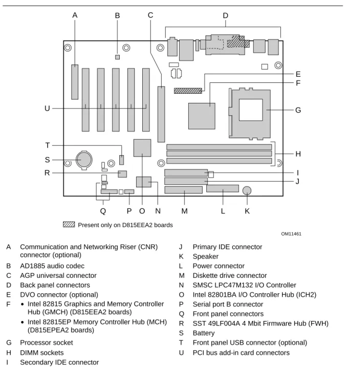
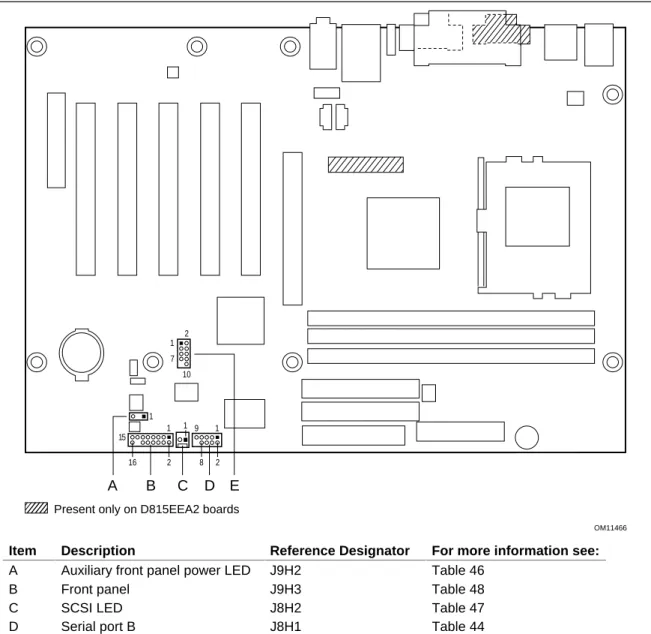
Figure 2 shows the location of the major components on the D815EEA2 and D815EPEA2 boards.
OM11461 D A C G E F O N Q P M L K B U S T R H I J
Present only on D815EEA2 boards
J Primary IDE connector A Communication and Networking Riser (CNR)
connector (optional) K Speaker
B AD1885 audio codec L Power connector
C AGP universal connector M Diskette drive connector
D Back panel connectors N SMSC LPC47M132 I/O Controller
E DVO connector (optional) O Intel 82801BA I/O Controller Hub (ICH2) P Serial port B connector
Q Front panel connectors
R SST 49LF004A 4 Mbit Firmware Hub (FWH) F • Intel 82815 Graphics and Memory Controller
Hub (GMCH) (D815EEA2 boards)
• Intel 82815EP Memory Controller Hub (MCH)
(D815EPEA2 boards) S Battery
G Processor socket T Front panel USB connector (optional)
H DIMM sockets U PCI bus add-in card connectors
I Secondary IDE connector
1.2.4 Block
Diagrams
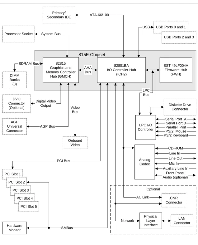
Figure 3 is a block diagram of the major functional areas of the D815EEA2 board.
Optional
815E Chipset
82801BA I/O Controller Hub
(ICH2) 82815 Graphics and Memory Controller Hub (GMCH) SST 49LF004A Firmware Hub (FWH) AHA Bus System Bus Processor Socket DIMM Banks (3) Primary/ Secondary IDE Diskette Drive Connector LPC I/O Controller PS/2 Keyboard PS/2 Mouse Parallel Port Serial Port A Serial Port B AGP Universal Connector ATA-66/100 USB AC Link AGP Bus LPC Bus SDRAM Bus
USB Ports 0 and 1 USB Ports 2 and 3
DVO Connector (Optional) Digital Video Output Auxiliary Line In Mic In Line Out CD-ROM Line In Front Panel Audio (optional) CNR Connector LAN Connector Physical Layer Interface PCI Slot 1 PCI Slot 2 PCI Slot 3 PCI Slot 4 PCI Slot 5 Network Analog Codec Onboard Video Video Bus
indicates connector or socket Hardware
Monitor SMBus
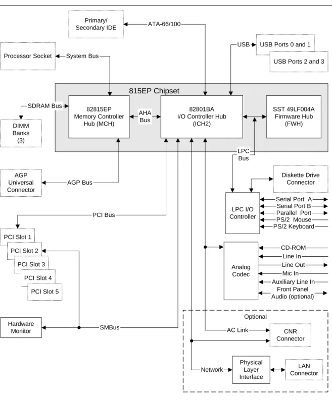
Figure 4 is a block diagram of the major functional areas of the D815EPEA2 board.
815EP Chipset
82801BA I/O Controller Hub
(ICH2) 82815EP Memory Controller Hub (MCH) SST 49LF004A Firmware Hub (FWH) AHA Bus System Bus Processor Socket DIMM Banks (3) Primary/ Secondary IDE Diskette Drive Connector LPC I/O Controller PS/2 Keyboard PS/2 Mouse Parallel Port Serial Port A Serial Port B AGP Universal Connector ATA-66/100 USB AGP Bus LPC Bus SDRAM Bus
USB Ports 0 and 1 USB Ports 2 and 3
Optional AC Link Auxiliary Line In Mic In Line Out CD-ROM Line In Front Panel Audio (optional) CNR Connector LAN Connector Physical Layer Interface Network Analog Codec
indicates connector or socket PCI Slot 1 PCI Slot 2 PCI Slot 3 PCI Slot 4 PCI Slot 5 Hardware Monitor SMBus PCI Bus
1.3 Online Support
To find information about… Visit this World Wide Web site:
Intel’s D815EEA2 and D815EPEA2 boards under “Product Info” or “Customer Support”
http://www.intel.com/design/motherbd
http://support.intel.com/support/motherboards/desktop Processor data sheets http://www.intel.com/design/litcentr
ICH2 addressing http://developer.intel.com/design/chipsets/datashts Custom splash screens http://intel.com/design/motherbd/gen_indx.htm Audio software and utilities http://www.intel.com/design/motherbd
LAN software and drivers http://www.intel.com/design/motherbd
1.4 Operating System Support
The D815EEA2 and D815EPEA2 boards support drivers for all of the onboard hardware and subsystems under the following operating systems:
• Windows† 98/98SE • Windows ME
• Windows NT† 4.0 • Windows 2000
For information about Refer to
Supported drivers Section 1.3
✏
NOTE
1.5 Design Specifications
Table 4 lists the specifications applicable to the D815EEA2 and D815EPEA2 boards, except for the AIMM and GPA entries, which apply only to the D815EEA2 board.
Table 4. Specifications
Reference Name
Specification Title
Version, Revision Date, and Ownership
The information is available from…
AC ’97 Audio Codec ’97 Revision 2.2, September 2000, Intel Corporation.
ftp://download.intel.com/ial/ scalableplatforms/ac97r22.pdf
ACPI Advanced Configuration and Power Interface Specification Version 2.0, July 27, 2000, Compaq Computer Corporation, Intel Corporation, Microsoft Corporation, Phoenix Technologies Limited, and Toshiba Corporation. http://www.teleport.com/~acpi/
AGP Accelerated Graphics Port Interface Specification Revision 2.0, May 4, 1998, Intel Corporation. http://www.agpforum.org/ AIMM (for Graphics Performance Accelerator cards)
AGP Inline Memory Module Revision 1.0, April 2000, Intel Corporation.
http://developer.intel.com/ technology/memory/aimm/ 298177.htm
AMI BIOS American Megatrends BIOS Specification
AMIBIOS 99, 1999,
American Megatrends, Inc.
http://www.amij.com/amibios/ bios.platforms.desktop.html
APM Advanced Power
Management BIOS Interface Specification
Version 1.2, February 1996, Intel Corporation and Microsoft Corporation. http://www.microsoft.com/ hwdev/busbios/amp_12.htm ATA/ ATAPI-5 Information Technology - AT Attachment with Packet Interface - 5 (ATA/ATAPI-5) Revision 3, February 29, 2000, Contact: T13 Chair, Seagate Technology. http://www.t13.org
ATX ATX Specification Version 2.03,
December 1998, Intel Corporation. http://www.formfactors.org/ developer/specs/atx/ atxspecs.htm CNR Communication and Network Riser (CNR) Specification Revision 1.1, October 18, 2000, Intel Corporation. http://developer.intel.com/ technology/cnr/index.htm continued
Table 4. Specifications (continued)
Reference Name
Specification Title
Version, Revision Date and Ownership
The information is available from…
DVI Digital Visual Interface DVI
Revision 1.0, April 2, 1999, Intel Corporation,
Silicon Image Incorporated, Compaq Computer Corporation, Fujitsu Limited,
Hewlett-Packard Company, and NEC Corporation.
http://www.ddwg.org/ downloads.html
EPP IEEE Std 1284.1-1997
(Enhanced Parallel Port)
Version 1.7, 1997,
Institute of Electrical and Electronic Engineers.
http://standards.ieee.org/ reading/ieee/std_public/ description/busarch/ 1284.1-1997_desc.html El Torito Bootable CD-ROM
Format Specification
Version 1.0, January 25, 1995,
Phoenix Technologies Limited and International Business Machines Corporation.
http://www.phoenix.com/ PlatSS/products/specs.html
GPA (see AIMM)
LPC Low Pin Count Interface Specification Version 1.0, September 29, 1997, Intel Corporation. http://www.intel.com/ design/chipsets/industry/ lpc.htm
PCI PCI Local Bus
Specification
Version 2.2, December 18, 1998, PCI Special Interest Group.
http://www.pcisig.com/
PCI Bus Power Management Interface Specification
Version 1.1, December 18, 1998, PCI Special Interest Group.
http://www.pcisig.com/
Plug and Play
Plug and Play BIOS Specification
Version 1.0a, May 5, 1994,
Compaq Computer Corporation, Phoenix Technologies Limited, and Intel Corporation.
http://www.microsoft.com/ hwdev/respec/
pnpspecs.htm
Table 4. Specifications (continued)
Reference Name
Specification Title
Version, Revision Date and Ownership
The information is available from…
SDRAM PC SDRAM Unbuffered DIMM Specification Revision 1.0, February 1998, Intel Corporation. http://www.intel.com/ technology/memory
PC SDRAM Specification Revision 1.7, November 1999, Intel Corporation. http://www.intel.com/ technology/memory PC Serial Presence Detect (SPD) Specification Revision 1.2B, November 1999, Intel Corporation. http://www.intel.com/ technology/memory
SMBIOS System Management BIOS
Version 2.3.1, March 16, 1999, American Megatrends Incorporated,
Award Software International Incorporated,
Compaq Computer Corporation, Dell Computer Corporation, Hewlett-Packard Company, Intel Corporation,
International Business Machines Corporation,
Phoenix Technologies Limited, and SystemSoft Corporation.
http://developer.intel.com/ ial/wfm/design/smbios
UHCI Universal Host Controller Interface Design Guide
Revision 1.1, March 1996, Intel Corporation.
http://www.usb.org/ developers
USB Universal Serial Bus Specification
Version 1.1, September 23, 1998,
Compaq Computer Corporation, Intel Corporation,
Microsoft Corporation, and NEC Corporation.
http://www.usb.org/ developers
WfM Wired for Management
Baseline Version 2.0, December 18, 1998, Intel Corporation. http://developer.intel.com/ ial/WfM/wfmspecs.htm
1.6 Processor
CAUTION
Use only the processors listed below. Use of unsupported processors can damage the board, the processor, and the power supply. See the Intel Desktop D815EEA2/D815EPEA2 Specification Update for the most up-to-date list of supported processors for the D815EEA2 and D815EPEA2 boards.
The D815EEA2 and D815EPEA2 boards both support a single Pentium III or Celeron processor. The system bus frequency is automatically selected. The D815EEA2 and D815EPEA2 boards support the processors listed in Table 5.
Table 5. Supported Processors
Type Designation System Bus Frequency L2 Cache Size
533EB, 600EB, 667, 733, 800B, 866, and 933 MHz
1.0 GHz
133 MHz 256 KB
Pentium III processor in an FC-PGA package
500E, 550E, 600E, 650, 700, 750, 800, and 850 MHz
100 MHz 256 KB
800 and 850 MHz 100 MHz 128 KB
Celeron processor in an
FC-PGA package 533A, 566, 600, 633, 667, 700, 733, and 766 MHz
66 MHz 128 KB
All supported onboard memory can be cached, up to the cachability limit of the processor. See the processor’s data sheet for cachability limits.
For information about Refer to
Product information on supported processors Section 1.3, page 19
1.7 System Memory
CAUTION
Before installing or removing memory, make sure that AC power is disconnected by unplugging the power cord from the computer. Failure to do so could damage the memory and the board.
✏
NOTE
Remove the AGP video card before installing or upgrading memory to avoid interference with the memory retention mechanism.
✏
NOTE
To be fully compliant with all applicable Intel® SDRAM memory specifications, the board should be populated with DIMMs that support the Serial Presence Detect (SPD) data structure. This allows the BIOS to read the SPD data and program the chipset to accurately configure memory settings for optimum performance. If non-SPD memory is installed, the BIOS will attempt to correctly configure the memory settings, but performance and reliability may be impacted or the DIMMs may not function under the determined frequency.
The D815EEA2 and D815EPEA2 boards both have three DIMM sockets and support the following memory features:
• 3.3 V (only) 168-pin SDRAM DIMMs with gold-plated contacts
• Unbuffered single-sided or double-sided DIMMs
• Maximum total system memory: 512 MB; minimum total system memory: 64 MB
• 133 MHz SDRAM or 100 MHz SDRAM
• Serial Presence Detect (SPD) and non-SPD memory
• Non-ECC and ECC DIMMs (ECC DIMMs will operate in non-ECC mode only)
• Suspend to RAM
When installing memory, note the following:
• Non-SPD DIMMs will always revert to a 100 MHz with 3-3-3 timing SDRAM bus.
• Mixing Non-SPD DIMMs with SPD DIMMs will always revert to a 100 MHz with 3-3-3 timing SDRAM bus.
• The BIOS will not initialize installed memory above 512 MB.
• Mixed memory speed configurations (133 and 100 MHz) will default to 100 MHz.
• 133 MHz SDRAM operation requires a 133 MHz system bus frequency processor.
• The board should be populated with no more than four rows of 133 MHz SDRAM (two double-sided or one double-double-sided plus two single-double-sided DIMMs).
• 100 MHz SDRAM may be populated with six rows of SDRAM (three double-sided DIMMs).
✏
NOTE
At boot, the BIOS displays a message indicating that any installed memory above 512 MB has not been initialized.
✏
NOTE
If more than four rows of 133 MHz SDRAM are populated, the BIOS will display a message indicating that it will initialize installed memory up to 512 MB at 100 MHz.
For information about Refer to
Obtaining the PC Serial Presence Detect (SPD) Specification Table 4, page 19
Table 6 lists the supported DIMM configurations.
Table 6. Supported Memory Configurations
DIMM Capacity Number of Sides SDRAM Density SDRAM Organization Front-side/Back-side Number of SDRAM devices 32 MB DS 16 Mbit 2 M x 8/2 M x 8 16 (Note 1) 32 MB SS 64 Mbit 4 M x 16/empty 4
48 MB DS 64/16 Mbit 4 M x 16/2 M x 8 12 (Notes 1 and 2)
64 MB DS 64 Mbit 4 M x 16/4 M x 16 8
64 MB SS 64 Mbit 8 M x 8/empty 8
64 MB SS 128 Mbit 8 M x 16/empty 4
96 MB DS 64 Mbit 8 M x 8/4 M x 16 12 (Notes 1 and 2)
96 MB DS 128/64 Mbit 8 M x 16/4 M x 16 8 (Notes 1 and 2)
128 MB DS 64 Mbit 8 M x 8/8 M x 8 16 (Note 1)
128 MB DS 128 Mbit 8 M x 16/8 M x 16 8 (Notes 1 and 2)
128 MB SS 128 Mbit 16 M x 8/empty 8
128 MB SS 256 Mbit 16 M x 16/empty 4
192 MB DS 128 Mbit 16 M x 8/8 M x 16 12 (Notes 1 and 2)
192 MB DS 128/64 Mbit 16 M x 8/8 M x 8 16 (Notes 1 and 2)
256 MB DS 128 Mbit 16 M x 8/16 M x 8 16 (Notes 1 and 2)
256 MB DS 256 Mbit 16 M x 16/16 M x 16 8 (Notes 1 and 2)
256 MB SS 256 Mbit 32 M x 8/empty 8
512 MB DS 256 Mbit 32 M x 8/32 M x 8 16 (Notes 1 and 2)
Notes:
1. If the number of SDRAM devices is greater than nine, the DIMM will be double sided.
2. Front side population/back side population indicated for SDRAM density and SDRAM organization.
3. In the second column, “DS” refers to double-sided memory modules (containing two rows of SDRAM) and “SS” refers to single-sided memory modules (containing one row of SDRAM).
1.8 Chipsets
This section describes the chipsets used by the D815EEA2 and D815EPEA2 boards:
• The D815EEA2 board uses the Intel 815E Chipset, described below.
• The D815EPEA2 board uses the Intel 815EP Chipset, described in Section 1.8.2, beginning on page 31.
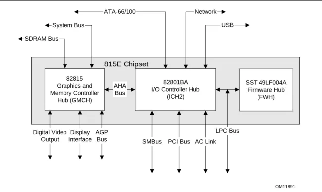
1.8.1 Intel
®815E Chipset
The Intel 815E chipset consists of the following devices:
• 82815 Graphics and Memory Controller Hub (GMCH) with Accelerated Hub Architecture (AHA) bus
• 82801BA I/O Controller Hub (ICH2) with AHA bus
• SST 49LF004A Firmware Hub (FWH)
The GMCH is a centralized controller for the system bus, the memory bus, the AGP bus, and the AHA bus. The ICH2 is a centralized controller for the board’s I/O paths. The FWH provides the nonvolatile storage of the BIOS.
The Intel 815E chipset provides the interfaces shown in Figure 5.
815E Chipset
82801BA I/O Controller Hub
(ICH2) 82815 Graphics and Memory Controller Hub (GMCH) SST 49LF004A Firmware Hub (FWH) AHA Bus System Bus ATA-66/100 USB AGP Bus OM11891 Network AC Link PCI Bus SMBus Digital Video Output SDRAM Bus LPC Bus Display Interface
Figure 5. Intel 815E Chipset Block Diagram
1.8.1.1 Intel
®82815 Graphics and Memory Controller Hub (GMCH)
The GMCH provides the following:
• An integrated Synchronous DRAM memory controller with autodetection of SDRAM
• An interface for a single AGP device or a Graphics Performance Accelerator (GPA) card
• An interface for an optional digital video output (DVO) connector for a flat panel, digital CRT, or TV-out
• Support for ACPI Rev. 2.0 and APM Rev. 1.2 compliant power management
1.8.1.2 Intel
®82801BA I/O Controller Hub (ICH2)
The ICH2 provides the following:
• 33 MHz PCI bus interface
• Support for up to six PCI master devices
• Low Pin Count (LPC) interface that supports an LPC-compatible I/O controller
• Support for two Master/DMA devices
• Integrated IDE controller that supports Ultra DMA (33 MB/sec) and ATA-66/100 mode (66 MB/sec, 100 MB/sec)
• Integrated LAN Media Access Controller
• Universal Serial Bus interface with two USB controllers providing four ports in a UHCI Implementation (additional USB ports provided with the optional SMSC LPC47M142 I/O controller)
• Power management logic for ACPI Rev. 1.0b compliance
• System Management Bus (SMBus clock and data lines also routed to PCI bus connector 2)
• Real-time clock with 256-byte battery-backed CMOS RAM
• AC ’97 digital link for audio codec, including:
AC ’97 2.1 compliance
Logic for PCM in, PCM out, and mic input
PCI functions for audio
Communication and Network Riser (CNR) interface
1.8.1.2.1 IDE Interfaces
The ICH2’s IDE controller has two independent bus-mastering IDE interfaces that can be independently enabled. The IDE interfaces support the following modes:
• Programmed I/O (PIO): CPU controls data transfer.
• 8237-style DMA: DMA offloads the CPU, supporting transfer rates of up to 16 MB/sec.
• Ultra DMA: DMA protocol on IDE bus supporting host and target throttling and transfer rates of up to 33 MB/sec.
• ATA-66: DMA protocol on IDE bus supporting host and target throttling and transfer rates of up to 66 MB/sec. ATA-66 protocol is similar to Ultra DMA and is device driver compatible.
• ATA-100: DMA protocol on IDE bus allows host and target throttling. The ICH2 ATA-100 logic can achieve read transfer rates up to 100 MB/sec and write transfer rates up to 88 MB/sec.
✏
NOTE
The IDE interfaces also support ATAPI devices (such as CD-ROM drives) and ATA devices using the transfer modes listed in Table 71 on page 121.
The BIOS supports Logical Block Addressing (LBA) and Extended Cylinder Head Sector (ECHS) translation modes. The drive reports the transfer rate and translation mode to the BIOS.
The D815EEA2 board supports Laser Servo (LS-120) diskette technology through its IDE interfaces. The LS-120 drive can be configured as a boot device by setting the BIOS Setup program’s Boot menu to one of the following:
• ARMD-FDD (ATAPI removable media device – floppy disk drive)
• ARMD-HDD (ATAPI removable media device – hard disk drive) For information about Refer to
The location of the IDE connectors Figure 15, page 73 The signal names of the IDE connectors Table 43, page 77 BIOS Setup program’s Boot menu Section 4.7, page 130
1.8.1.2.2 USB
The ICH2 contains two separate USB controllers. The D815EEA2 board has four USB ports; one USB peripheral can be connected to each port. For more than four USB devices, an external hub can be connected to any of the ports. The D815EEA2 board fully supports the Universal Hub Controller Interface (UHCI).
In the standard configuration, the D815EEA2 board’s four USB ports are implemented with stacked back panel connectors, routed through the ICH2, as shown in Figure 6.
With the optional SMSC LPC47M142 I/O controller, the D815EEA2 board supports up to seven USB ports. The SMSC LPC47M142 I/O controller provides four ports: two ports implemented with stacked back panel connectors and two ports routed to the optional front panel USB connector at location J8F1. The ICH2 provides three ports: two ports are implemented with stacked back panel connectors and the other port is accessible through a CNR add-in card, as shown in Figure 6. The D815EEA2 board fully supports the Universal Hub Controller Interface (UHCI).
82801BA I/O Controller Hub
(ICH2)
OM11892
USB ports 0 and 1
USB ports 2 and 3 USB
Back panel USB connectors
Back panel USB connectors
82801BA I/O Controller Hub
(ICH2)
USB ports 0 and 2
CNR connector USB
Back panel USB connectors
Standard Configuration
Optional Configuration
SMSC LPC47M142 LPC Bus I/O Controller
USB ports 1 and 3
USB ports 4 and 5 USB
Back panel USB connectors
Front panel USB connector USB
USB port accesible through a USB connector on an optional CNR add-in card
Figure 6. USB Port Configurations
✏
NOTE
Computer systems that have an unshielded cable attached to a USB port may not meet FCC Class B requirements, even if no device or a low-speed USB device is attached to the cable. Use shielded cable that meets the requirements for full-speed devices.
For information about Refer to
The location of the USB connectors on the back panel Figure 13, page 64 The signal names of the back panel USB connectors Table 21, page 65 The location of the optional front panel USB connector Figure 16, page 78 The signal names of the optional front panel USB connector Table 45, page 79
1.8.1.2.3 Real-Time Clock, CMOS SRAM, and Battery
The real-time clock provides a time-of-day clock and a multicentury calendar with alarm features. The real-time clock supports 256 bytes of battery-backed CMOS SRAM in two banks that are reserved for BIOS use.
A coin-cell battery (CR2032) powers the real-time clock and CMOS memory. When the computer is not plugged into a wall socket, the battery has an estimated life of three years. When the
computer is plugged in, the standby current from the power supply extends the life of the battery. The clock is accurate to ± 13 minutes/year at 25 ºC with 3.3 VSB applied.
The time, date, and CMOS values can be specified in the BIOS Setup program. The CMOS values can be returned to their defaults by using the BIOS Setup program.
✏
NOTE
If the battery and AC power fail, custom defaults, if previously saved, will be loaded into CMOS SRAM at power-on.
1.8.1.3 SST 49LF004A 4 Mbit Firmware Hub (FWH)
1.8.2 Intel
®815EP Chipset
The Intel 815EP chipset consists of the following devices:
• 82815EP Memory Controller Hub (MCH) with Accelerated Hub Architecture (AHA) bus
• 82801BA I/O Controller Hub (ICH2) with AHA bus
• SST 49LF004A Firmware Hub (FWH)
The MCH is a centralized controller for the system bus, the memory bus, the AGP bus, and the AHA bus. The ICH2 is a centralized controller for the board’s I/O paths. The FWH provides the nonvolatile storage of the BIOS.
The Intel 815EP chipset provides the interfaces shown in Figure 7.
815EP Chipset
82801BA I/O Controller Hub
(ICH2) 82815EP Memory Controller Hub (MCH) SST 49LF004A Firmware Hub (FWH) AHA Bus System Bus ATA-66/100 USB AGP Bus OM11318 Network AC Link PCI Bus SMBus SDRAM Bus LPC Bus
Figure 7. Intel 815EP Chipset Block Diagram
For information about Refer to
The Intel 815EP chipset http://developer.intel.com/design/chipsets/815ep The resources used by the chipset Chapter 2
1.8.2.1 Intel
®82815EP Memory Controller Hub (MCH)
The MCH provides the following:
• An integrated Synchronous DRAM memory controller with autodetection of SDRAM
• An interface for a single AGP device
• Support for ACPI Rev. 2.0 and APM Rev. 1.2 compliant power management
1.8.2.2 Intel 82801BA I/O Controller Hub (ICH2)
The ICH2 provides the following:
• 33 MHz PCI bus interface
• Support for up to six PCI master devices
• Low Pin Count (LPC) interface that supports an LPC-compatible I/O controller
• Support for two Master/DMA devices
• Integrated IDE controller that supports Ultra DMA (33 MB/sec) and ATA-66/100 mode (66 MB/sec, 100 MB/sec)
• Integrated LAN Media Access Controller
• Universal Serial Bus interface with two USB controllers providing four back panel ports in a UHCI Implementation (additional USB ports provided with the optional SMSC LPC47M142 I/O controller)
• Power management logic for ACPI Rev. 1.0b compliance
• System Management Bus (SMBus clock and data lines also routed to PCI bus connector 2)
• Real-time clock with 256-byte battery-backed CMOS RAM
• AC ’97 digital link for audio codec, including:
AC ’97 2.1 compliance
Logic for PCM in, PCM out, and mic input
PCI functions for audio
Communication and Network Riser (CNR) interface
1.8.2.2.1 IDE Interfaces
The ICH2’s IDE controller has two independent bus-mastering IDE interfaces that can be independently enabled. The IDE interfaces support the following modes:
• Programmed I/O (PIO): CPU controls data transfer.
• 8237-style DMA: DMA offloads the CPU, supporting transfer rates of up to 16 MB/sec.
• Ultra DMA: DMA protocol on IDE bus supporting host and target throttling and transfer rates of up to 33 MB/sec.
• ATA-66: DMA protocol on IDE bus supporting host and target throttling and transfer rates of up to 66 MB/sec. ATA-66 protocol is similar to Ultra DMA and is device driver compatible.
• ATA-100: DMA protocol on IDE bus allows host and target throttling. The ICH2 ATA-100 logic can achieve read transfer rates up to 100 MB/sec and write transfer rates up to 88 MB/sec.
✏
NOTE
The IDE interfaces also support ATAPI devices (such as CD-ROM drives) and ATA devices using the transfer modes listed in Table 71 on page 121.
The BIOS supports Logical Block Addressing (LBA) and Extended Cylinder Head Sector (ECHS) translation modes. The drive reports the transfer rate and translation mode to the BIOS.
The D815EEA2 board supports Laser Servo (LS-120) diskette technology through its IDE interfaces. The LS-120 drive can be configured as a boot device by setting the BIOS Setup program’s Boot menu to one of the following:
• ARMD-FDD (ATAPI removable media device – floppy disk drive)
• ARMD-HDD (ATAPI removable media device – hard disk drive) For information about Refer to
The location of the IDE connectors Figure 15, page 73 The signal names of the IDE connectors Table 43, page 77
BIOS Setup program’s Boot menu Section 4.7, page 130
1.8.2.2.2 USB
The ICH2 contains two separate USB controllers. The D815EPEA2 board has four USB ports; one USB peripheral can be connected to each port. For more than four USB devices, an external hub can be connected to any of the ports. The D815EPEA2 board fully supports the Universal Hub Controller Interface (UHCI).
In the standard configuration, the D815EPEA2 board’s four USB ports are implemented with stacked back panel connectors, routed through the ICH2, as shown in Figure 8.
With the optional SMSC LPC47M142 I/O controller, the D815EPEA2 board supports up to seven USB ports. The SMSC LPC47M142 I/O controller provides four ports: two ports implemented with stacked back panel connectors and two ports routed to the optional front panel USB connector at location J8F1. The ICH2 provides three ports: two ports are implemented with stacked back panel connectors and the other port is accessible through a CNR add-in card, as shown in Figure 8. The D815EPEA2 board fully supports the Universal Hub Controller Interface (UHCI).
82801BA I/O Controller Hub
(ICH2)
OM11892
USB ports 0 and 1
USB ports 2 and 3 USB
Back panel USB connectors
Back panel USB connectors
82801BA I/O Controller Hub
(ICH2)
USB ports 0 and 2
CNR connector USB
Back panel USB connectors
Standard Configuration
Optional Configuration
SMSC LPC47M142 LPC Bus I/O Controller
USB ports 1 and 3
USB ports 4 and 5 USB
Back panel USB connectors
Front panel USB connector USB
USB port accesible through a USB connector on an optional CNR add-in card
Figure 8. USB Port Configurations
✏
NOTE
Computer systems that have an unshielded cable attached to a USB port may not meet FCC Class B requirements, even if no device or a low-speed USB device is attached to the cable. Use shielded cable that meets the requirements for full-speed devices.
For information about Refer to
The location of the USB connectors on the back panel Figure 13, page 64 The signal names of the back panel USB connectors Table 21, page 65 The location of the optional front panel USB connector Figure 16, page 78 The signal names of the optional front panel USB connector Table 45, page 79
1.8.2.2.3 Real-Time Clock, CMOS SRAM, and Battery
The real-time clock provides a time-of-day clock and a multicentury calendar with alarm features. The real-time clock supports 256 bytes of battery-backed CMOS SRAM in two banks that are reserved for BIOS use.
A coin-cell battery (CR2032) powers the real-time clock and CMOS memory. When the computer is not plugged into a wall socket, the battery has an estimated life of three years. When the
computer is plugged in, the standby current from the power supply extends the life of the battery. The clock is accurate to ± 13 minutes/year at 25 ºC with 3.3 VSB applied.
The time, date, and CMOS values can be specified in the BIOS Setup program. The CMOS values can be returned to their defaults by using the BIOS Setup program.
✏
NOTE
If the battery and AC power fail, custom defaults, if previously saved, will be loaded into CMOS SRAM at power-on.
1.8.2.3 SST 49LF004A 4 Mbit Firmware Hub (FWH)
1.9 I/O Controller
The D815EEA2 and D815EPEA2 boards support either of two I/O controllers:
• The standard SMSC LPC47M132 I/O controller or
• The optional SMSC LPC47M142 I/O controller Both I/O controllers provide the following features:
• Low pin count (LPC) interface
• 3.3 V operation
• Two serial ports
• One parallel port with Extended Capabilities Port (ECP) and Enhanced Parallel Port (EPP) support
• Serial IRQ interface compatible with serialized IRQ support for PCI systems
• PS/2-style mouse and keyboard interfaces
• Interface for one 1.2 MB, 1.44 MB, or 2.88 MB diskette drive
• Intelligent power management, including a programmable wake up event interface
• PCI power management support
• Fan control
One fan control output
Two fan tachometer inputs
The optional SMSC LPC47M142 I/O controller provides an additional USB hub. The BIOS Setup program provides configuration options for the I/O controller.
For information about Refer to
The USB hubs on the D815EEA2 board Section 1.8.1.2.2, page 28 The USB hubs on the D815EPEA2 board Section 1.8.2.2.2, page 33 SMSC LPC47M132 and LPC47M142 I/O controllers http://www.smsc.com
1.9.1 Serial
Ports
The D815EEA2 and D815EPEA2 boards each have two serial ports. Serial port A is located on the back panel. Serial port B is accessible using the connector at location J8H1. The serial ports’ NS16C550-compatible UARTs support data transfers at speeds up to 115.2 kbits/sec with BIOS support. The serial ports can be assigned as COM1 (3F8h), COM2 (2F8h), COM3 (3E8h), or COM4 (2E8h).
For information about Refer to
The location of the serial port A connector Figure 13, page 64 The signal names of the serial port A connector Table 24, page 66 The location of the serial port B connector Figure 16, page 78 The signal names of the serial port B connector Table 44, page 79
1.9.2 Parallel
Port
The connector for the parallel port is a 25-pin D-Sub connector located on the back panel. In the BIOS Setup program, the parallel port can be set to the following modes:
• Output only (PC-AT†-compatible mode) • Bi-directional (PS/2 compatible)
• EPP
• ECP
For information about Refer to
The location of the parallel port connector Figure 13, page 64 The signal names of the parallel port connector Table 23, page 65
Setting the parallel port’s mode Table 69, page 118
1.9.3 Diskette Drive Controller
The I/O controller supports one diskette drive that is compatible with the 82077 diskette drive controller and supports both PC-AT and PS/2 modes.
For information about Refer to
The location of the diskette drive connector Figure 15, page 73 The signal names of the diskette drive connector Table 42, page 77 The supported diskette drive capacities and sizes Table 72, page 123
1.9.4 Keyboard and Mouse Interface
PS/2 keyboard and mouse connectors are located on the back panel. The +5 V lines to these connectors are protected with a thermistor, which limits the current to a specified amperage.
✏
NOTE
The keyboard is supported in the bottom PS/2 connector and the mouse is supported in the top PS/2 connector. Power to the computer should be turned off before a keyboard or mouse is connected or disconnected.
The keyboard controller contains the AMI keyboard and mouse controller code, provides the keyboard and mouse control functions, and supports password protection for power-on/reset. A power-on/reset password can be specified in the BIOS Setup program.
The keyboard controller also supports the hot-key sequence <Ctrl><Alt><Del> for a software reset (operating system dependent). This key sequence resets the computer’s software by jumping to the beginning of the BIOS code and running the power-on self-test (POST).
For information about Refer to
The location of the keyboard and mouse connectors Figure 13, page 64 The signal names of the keyboard and mouse connectors Table 20, page 65 Overcurrent protection for back panel connectors Table 19, page 65
1.10 Graphics Subsystems
This section describes the graphics subsystems used by the D815EEA2 and D815EPEA2 boards:
• The D815EEA2 board uses the Intel 815E graphics subsystem, described below.
• The D815EPEA2 board uses the Intel 815EP graphics subsystem, described in Section 1.10.2, beginning on page 42.
1.10.1 Intel 815E Graphics Subsystem
The 815E chipset, used on the D815EEA2 board, contains two separate, mutually exclusive graphics options. Either the integrated graphics controller (contained within the 82815 GMCH) is used, or an add-in AGP adapter can be used.
The GMCH includes an integrated display cache SDRAM controller that supports a Graphics Performance Accelerator (GPA) card. The GPA card is a 32-bit 133 MHz 4 MB SDRAM array for enhanced integrated 2D and 3D graphics performance. This interface is multiplexed between the display cache interface and the AGP connector. When an AGP card is installed, the integrated graphics controller is disabled and the display cache interface is not used.
For information about Refer to
GPA support Section 1.10.1.3.1, page 41
1.10.1.1 Integrated Graphics Controller
The GMCH features the following:
• Integrated graphics controller
3-D Hyperpipelined architecture
Full 2-D hardware acceleration
Motion video acceleration
• 3-D graphics visual and texturing enhancement
• Display
Integrated 24-bit 230 MHz RAMDAC
Display Data Channel Standard, Version 3.0, Level 2B protocols compliant
• Video
Hardware motion compensation for software MPEG2 decode
Software DVD at 30 fps
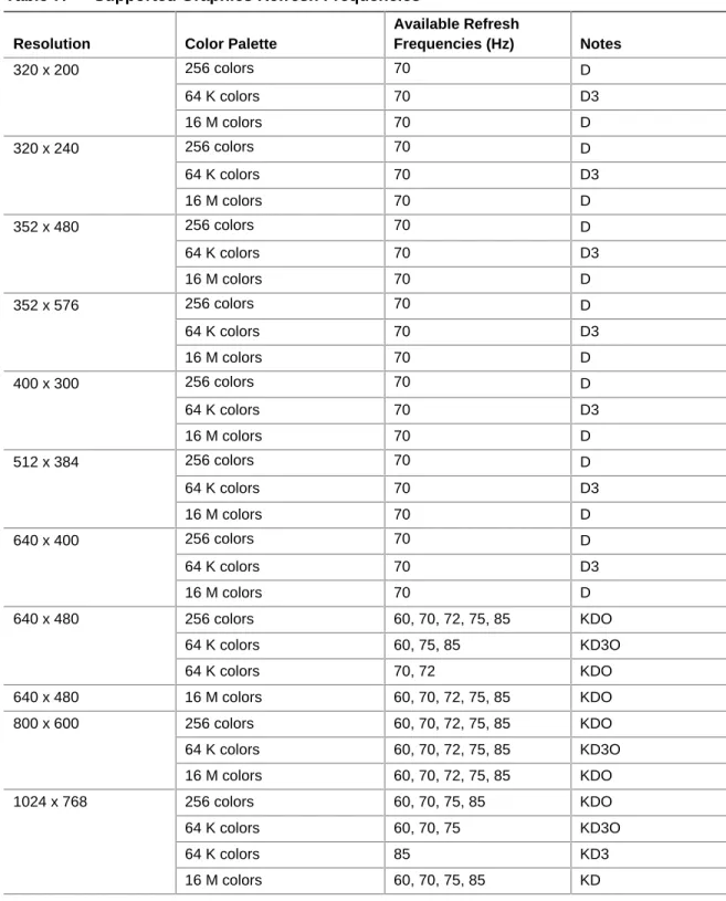
Table 7 lists the refresh frequencies supported by the graphics subsystem.
Table 7. Supported Graphics Refresh Frequencies
Resolution Color Palette
Available Refresh Frequencies (Hz) Notes 256 colors 70 D 64 K colors 70 D3 320 x 200 16 M colors 70 D 256 colors 70 D 64 K colors 70 D3 320 x 240 16 M colors 70 D 256 colors 70 D 64 K colors 70 D3 352 x 480 16 M colors 70 D 256 colors 70 D 64 K colors 70 D3 352 x 576 16 M colors 70 D 256 colors 70 D 64 K colors 70 D3 400 x 300 16 M colors 70 D 256 colors 70 D 64 K colors 70 D3 512 x 384 16 M colors 70 D 256 colors 70 D 64 K colors 70 D3 640 x 400 16 M colors 70 D 256 colors 60, 70, 72, 75, 85 KDO 64 K colors 60, 75, 85 KD3O 640 x 480 64 K colors 70, 72 KDO 640 x 480 16 M colors 60, 70, 72, 75, 85 KDO 256 colors 60, 70, 72, 75, 85 KDO 64 K colors 60, 70, 72, 75, 85 KD3O 800 x 600 16 M colors 60, 70, 72, 75, 85 KDO 256 colors 60, 70, 75, 85 KDO 64 K colors 60, 70, 75 KD3O 64 K colors 85 KD3 1024 x 768 16 M colors 60, 70, 75, 85 KD continued
Table 7. Supported Graphics Refresh Frequencies (continued)
Resolution Color Palette
Available Refresh Frequencies (Hz) Notes 256 colors 60, 70, 72, 75 KDO 256 colors 85 KD 64 K colors 60, 70 KD3O 64 K colors 72, 75, 85 KD3 16 M colors 60 KDO 1152 x 864 16 M colors 75, 85 KD
256 colors 60 (reduced blanking) KDOF
64 K colors 60 (reduced blanking) KD3F 1280 x 768
16 M colors 60 (reduced blanking) KDF
256 colors 60 KDO 256 colors 70, 72, 75, 85 KD 64 K colors 60, 70, 72, 75, 85 KD3 1280 x 1024 16 M colors 60, 70, 75, 85 KD 1600 x 1200 256 colors 60, 70, 72, 75 KD Notes: K = Desktop D = DirectDraw†
3 = Direct3D† and OpenGL† O = Overlay
F = Digital Display Device only. A mode will be supported on both analog CRTs and digital display devices (KD3O applies to both types of displays), unless indicated otherwise.
For information about Refer to
Obtaining graphics software and utilities Section 1.3, page 19
1.10.1.2 Digital Video Output (DVO) Connector (Optional)
The D815EEA2 board routes the Intel 82815 GMCH DVO port to an optional onboard 40-pin DVO connector. The DVO connector can be cabled to a DVI or TV out card to enable digital displays or TV out functionality. The Digital Visual Interface (DVI) specification provides a high-speed digital connection for visual data types when using the integrated graphics controller. This interface is active only when the integrated graphics controller is enabled.
The DVI interface allows interfacing with a discrete Transmission Minimized Differential Signaling (TMDS) transmitter to enable platform support for DVI compliant digital displays or with a discrete TV encoder for TV out functionality.
For information about Refer to
The location of the DVO connector Figure 14, page 69 The signal names of the DVO connector Table 32, page 71
1.10.1.3 AGP Universal Connector
✏
NOTE
Install memory in the DIMM sockets prior to installing the AGP video card to avoid interference with the memory retention mechanism.
The AGP universal connector supports either:
• Graphics Performance Accelerator (GPA) cards with 133 MHz SDRAM display cache
• 1x, 2x, or 4x AGP add-in cards with either 3.3 V or 1.5 V I/O For information about Refer to
The location of the AGP universal connector Figure 15, page 73 The signal names of the AGP universal connector Table 41, page 76
1.10.1.3.1 Graphics Performance Accelerator (GPA) Support
The Intel 815E GMCH display cache is a single channel 32-bit wide SDRAM interface. The 4 MB display cache resides on a GPA card that plugs into the AGP connector. The BIOS detects a GPA card if present in the AGP port and initializes it as display cache memory. When a GPA card is initialized, the BIOS allocates 1 MB of system memory to support the internal display device operation.
1.10.1.3.2 Dynamic Video Memory Technology (DVMT)
DVMT enables enhanced graphics and memory performance through Direct AGP, and highly efficient memory utilization. DVMT ensures the most efficient use of all available memory for maximum 2D/3D graphic performance. DVMT is implemented on the D815EEA2 board with a GPA (Graphics Performance Accelerator) card installed in the AGP connector.
✏
NOTE
In earlier documentation, the GPA card was referred to as the AGP Inline Memory Module (AIMM).
DVMT uses 1 MB of system physical memory for compatibility with legacy applications. An example of this would be when using VGA graphics under DOS. Once loaded, the operating system and graphics drivers allocate the buffers needed for performing graphics functions. When the 4 MB GPA card is installed, the Z-buffer and GDI data are managed directly from this dedicated graphics memory thereby avoiding operating system memory manager calls and improving performance.
At system BIOS POST, the BIOS displays either the amount of physical memory allocated for display cache or the size of the GPA card (4 MB) if installed. Operating systems such as
Windows NT 4.0 and Windows 2000 may display the maximum amount of frame buffer memory possible based on the system memory configuration.
✏
NOTE
The use of DVMT requires operating system driver support. For information about Refer to
Obtaining the DVMT white paper http://developer.intel.com/design/chipsets/815e/ Obtaining the AIMM specification Table 4, page 20
1.10.1.3.3 AGP Add-in Card Support
AGP is a high-performance interface for graphics-intensive applications, such as 3D applications. While based on the PCI Local Bus Specification, Rev. 2.1, AGP is independent of the PCI bus and is intended for exclusive use with graphical display devices. AGP overcomes certain limitations of the PCI bus related to handling large amounts of graphics data with the following features:
• Pipelined memory read and write operations that hide memory access latency
• Demultiplexing of address and data on the bus for nearly 100 percent efficiency For information about Refer to
Obtaining the Accelerated Graphics Port Interface Specification Table 4, page 20
1.10.2 Intel 815EP Graphics Subsystem
✏
NOTE
Install memory in the DIMM sockets prior to installing the AGP video card to avoid interference with the memory retention mechanism.
The Intel 815EP chipset, used on the D815EPEA2 board, provides an AGP universal connector which supports a 1x, 2x, or 4x AGP add-in card with either 3.3 V or 1.5 V I/O.
AGP is a high-performance interface for graphics-intensive applications, such as 3D applications. While based on the PCI Local Bus Specification, Rev. 2.1, AGP is independent of the PCI bus and is intended for exclusive use with graphical display devices. AGP overcomes certain limitations of the PCI bus related to handling large amounts of graphics data with the following features:
• Pipelined memory read and write operations that hide memory access latency
• Demultiplexing of address and data on the bus for nearly 100 percent efficiency For information about Refer to
The location of the AGP universal connector Figure 15, page 73 The signal names of the AGP universal connector Table 41, page 76 Obtaining the Accelerated Graphics Port Interface Specification Table 4, page 20
1.11 Audio Subsystem
The D815EEA2 and D815EPEA2 boards both include an Audio Codec ’97 (AC ’97) compatible audio subsystem consisting of these devices:
• Intel 82801BA I/O Controller Hub (ICH2)
• Analog Devices AD1885 analog codec
1.11.1 AD1885 Audio Codec
The AD1885 is a fully AC ’97 compliant codec. The codec’s features include:
• > 90 dB signal-to-noise ratio sound quality
• Power management support for APM 1.2 and ACPI 1.0 (driver dependant)
• Playback sample rates up to 48 kHz
• 16 bit stereo full-duplex codec
• Software compatible with Windows 98 SE, Windows 2000, Windows NT 4.0, and Windows Millennium (Me)
• Full-duplex operation at asynchronous hardware record/playback samples rates
• Frequency response: 20 Hz to 20 kHz (± 0.1 dB)
Figure 9 is a block diagram of the D815EEA2 and D815EPEA2 boards’ audio subsystem, including the Intel 82801BA ICH2 digital controller, the AD1885 analog codec, and the audio connectors.
82801BA I/O Controller Hub
(ICH2) OM11888 AC ’97 Link CD-ROM Line In Audio In Mic In
Front Panel Audio (optional) Line Out
Analog Devices AD1885 Analog Codec
Figure 9. Block Diagram of Audio Subsystem
For information about Refer to
Obtaining the AC ’97 specification Table 4, page 19
1.11.2 Audio
Connectors
The audio connectors include the following:
• Front panel audio (optional):
Mic in
Line out
• ATAPI-style connectors:
CD-ROM
• Back panel audio connectors:
Line in
Line out
Mic in
For information about Refer to
The back panel audio connectors Section 2.8.1, page 64
1.11.2.1 Front Panel Audio Connector (Optional)
A 2 x 5-pin connector for routing mic in and line out to the front panel. For information about Refer to
The location of the optional front panel audio connector Figure 14, page 69 The signal names of the optional front panel audio connector Table 30, page 70
✏
NOTE
The front panel audio connector is alternately used as a jumper block for routing audio signals. Refer to Section 2.9.1 on page 82 for more information.
1.11.2.2 ATAPI CD-ROM Connector
A 1 x 4-pin ATAPI-style connector connects an internal ATAPI CD-ROM drive to the audio mixer. For information about Refer to
The location of the ATAPI CD-ROM connector Figure 14, page 69 The signal names of the ATAPI CD-ROM connector Table 31, page 70
1.11.2.3 Auxiliary Line In Connector
A 1 x 4-pin ATAPI-style connector connects the left and right channel signals of an internal audio device to the audio subsystem.
For information about Refer to
The location of the auxiliary line in connector Figure 14, page 69 The signal names of the auxiliary line in connector Table 29, page 70