Volume 1, Issue 7, September 2012
Efficient Role of Electro-optic Modulators in
Lightwave Optical Access Communication
Networks
Dr. Ahmed Nabih Zaki Rashed
Electronics and Electrical Communications Engineering Department Faculty of Electronic Engineering, Menouf 32951, Menoufia University, EGYPT
Abstract-In the present paper, we have been modeled parametrically and numerically the high speed of materials based electrooptic (EO) modulators in advanced optical communication systems. The modulated bandwidth is deeply and parametrically studied over wide ranges of the affecting sets of parameters via specially designed software which processes the interaction of causes and effects. The design parameters of the lumped circuit have been processed over large operating requirements. Lithium niobate (LiNbO3) external modulators can also offer pure phase modulation in coherent systems and can realize various optical signal processors. As the bit rate of optical network systems becomes higher, it becomes more difficult to drive a modulator with a high voltage. Therefore, reduction of the driving voltage of an LiNbO3 modulator with a broadband characteristic is an extremely important issue for realizing future high speed optical transmission systems. Moreover polymer electrooptic devices have been extensively studied and explored due to its intrinsic advantages over conventional materials such as high speed operation, compatibility with other materials and substrates.
Index Terms- Electrooptic devices, electrooptic modulation, optical polymers, Lithium niobat, slab and rib waveguides.
I.INTRODUCTION
Present communication technology relies on fiber optic systems which include light sources such as a laser, optical fiber, integrated optical components such as modulators and switches, and optical detectors. The lasers and detectors are fabricated using semiconductor materials, and the integrated optical components are generally fabricated using electrooptic single crystal materials such as lithium niobate (LiNbO3). Among the integrated optical components, the
contribution from electrooptic modulators using LiNbO3
waveguide structures has been significant in the last several decades due to their high-speed [1]. The essential requirements for efficient electrooptic modulation are low half-wave (switching) voltage and broad 3-dB modulation bandwidth. High-speed traveling-wave electro optic modulators are very important devices because of their applications in many optoelectronic fields, such as telecommunication, optical signal processing, and optical measurement. With the increasing demand for broadband communication, many studies on the high-speed electro optic modulators have been carried out for optical communication system [2]. In addition, the precise control of the frequency responses of high-speed electro optic modulators has been required for the new generation optical fiber communication systems. In a standard traveling-wave electrooptic modulator, the frequency response of the modulation index is restricted by two effects: the velocity mismatching between the lightwave and modulation
microwave and the loss of modulation microwave in the traveling-wave electrodes [3].
Electrooptic modulators have a number of telecommunication and scientific applications, including analog optical links, optical signal processing (OSP), and frequency comb generation [4]. These types of modulators have an enhanced modulation response within a finite bandwidth of typically a few gigahertz around resonance. Ring resonators made from EO polymer materials have certain advantages over other material choices such as LiNbO3, most notably the low microwave/optical velocity
mismatch allowing for simple design of high-speed modulation devices. For instance, demonstrations driving an EO polymer Mach–Zehnder (MZ) modulator beyond 100 GHz have been reported previously [5]. In addition, the photolithographic fabrication capabilities of EO polymer enable easy integration of complex OSP structures. In semiconductor electrooptic modulators (EOMs), high-modulation efficiency can be achieved by applying the modulating voltage to a reverse-bias diode whose depletion region forms the waveguide core. This arrangement can be accomplished on GaAs by etching a ridge into a p-i-n doped slab waveguide that is composed of epitaxial GaAs–AlGaAs layers. Usually, in order to minimize waveguide loss, this ridge is shallow-etched such that only the upper cladding of the planar waveguide is penetrated. Using this approach, low voltage, low-loss modulators optimized for both 10 and 40Gbit/sec applications have been demonstrated [5] and have been commercially available for some time. In more complex optical circuits, however, the weak horizontal optical confinement of the shallow-etched waveguide can be problematic. In particular, the implementation of waveguide bends and the avoidance of optical crosstalk require both careful design and accurate fabrication [6].
In the present study, LiNbO3, and Polymer electrooptic
external modulators have been developed for extensive use in high speed and long distance optical fiber transmission systems. This is because they can offer the advantages of modulation exceeding multi Gbit/sec combined with a low driving voltage, and they can eliminate the dynamic laser wavelength chirping which limits the span-rate system product due to their fiber dispersion characteristics.
II.TYPES OF MODULATION SCHEMES
Volume 1, Issue 7, September 2012 shown in Fig. 1, is such a device that converts the electrical
signal to the optical one and passed it to the amplification process stage.
Fig. 1. Electooptic modulator function in the transmitter system.
In addition, high bandwidth optical modulation has also applications in fiber optic radio frequency signal transmission and optoelectronic signal processing [7].
II.1.DIRECT MODULATION SCHEME
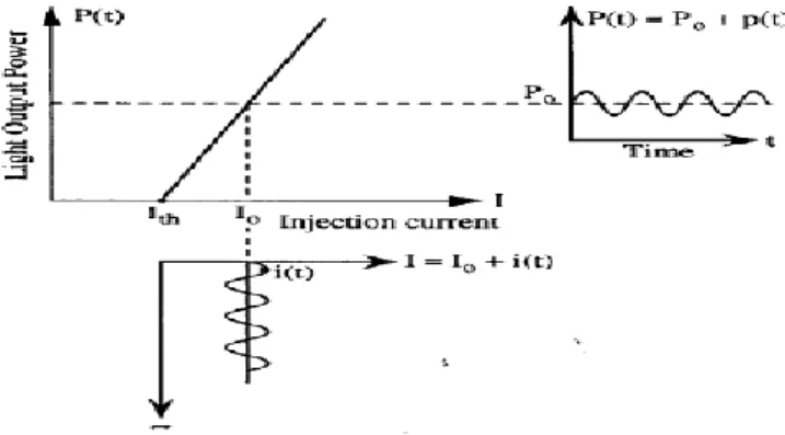
The most straightforward method for modulation is to directly modulate the laser source. Due to the requirements of bandwidth and efficiency, only semiconductor lasers are of practical interest for direct modulation A unique feature of semiconductor lasers is that the semiconductor laser can be modulated directly by modulating the excitation current. As shown in Fig. 2, for a semiconductor laser, the output power of light intensity increases linearly with the injection current above threshold.
Fig. 2. Transition function of a current modulated semiconductor laser
For an injection current I = I0 + i (t), the optical output
power is P(t) =P0+p(t), where (I0,P0) is the bias point for the
direct modulation of the semiconductor laser [8]. Using this feature, the direct modulation scheme can be configured as shown in Fig. 3.
Fig. 3. Direct modulation scheme.
However, when the modulation frequency increases toward the relaxation resonance frequency of a semiconductor laser, both the relative intensity noise and distortions increase rapidly [8]. This severely limits the feasibility of direct modulation for a higher frequency. The large frequency chirp also precludes the direct modulation for long-distance communications systems.
II.2.EXTERNAL MODULATION SCHEME
At bit rates of 10 Gbit/s or higher, the frequency chirp imposed by direct modulation becomes large enough that direct modulation of semiconductor laser is rarely used [9]. Unlike direct modulation, external modulation has been shown to have superior performance for wide bandwidth optical fiber communications, however with
the potential disadvantages of adding system complexity and cost.
Fig. 4. External modulation scheme.
As shown in Fig. 4, for a high-speed transmitter, the laser is biased at a constant current to provide the continuous wave (CW) output, and an external optical modulator placed next to the laser converts the CW light into a data coded pulse train with correct modulation format. In the external modulation scheme, the light output passes through a material whose optical properties can be modified by an applied external electric field. External optical modulators with bandwidths greater than 10 GHz are typically fabricated from the electro-optic crystal LiNbO3,
electro-optic polymers or III-V semiconductor compounds. Some of these devices have shown modulation frequencies in excess of 40 GHz [10].
III.LUMPED ELEMENT CIRCUIT MODEL
At frequencies where the wavelength is several orders of magnitude larger than the greatest dimensions of the circuit or system being examined, conventional circuit elements such as capacitors, inductors and resistors are the basic building blocks for the circuits or systems. The description or analysis of such circuits may be adequately carried out in terms of loop currents and node voltages without consideration of propagation effects.
Volume 1, Issue 7, September 2012 IV.THEORETICAL MODEL ANALYSIS
Both the input power Pi and the output power P0 of the
modulator are given by [11]:
, 2 L m in R V
P Watt (1)
, 4 06 332
2 2 0 r n L A P m m
Watt (2)
Where Vm is the modulating voltage, RL is the load
resistance, Γm is the peak retardation of the modulating
voltage, ε =ε0 . εr is the dielectric constant at the modulation
frequency ω0, A is the cross-section area, υ is the
modulation bandwidth, Lm is the modulator length, n0 is the
refractive index of the material, r63 is the elect-optic
coefficient. The resonance frequency ωr and the angular
bandwidth ω can be expressed as the following: , 1 2 2 2 r L C L
r
(3)
, 1
C R
(4)
Where r is the linear ratio of ON power to OFF power, R is the resistance of the lumped circuit, C is the capacitance of the lumped circuit. Also we have in the electrooptic modulators, the peak retardation of modulation voltage is given by the following formula:
, V Vm m (5)
Where Vπ is the voltage required to change the output light intensity from its maximum value to its minimum value or modulator half wave voltage can be expressed as [11].
, 2n30r33
V (6)
Assuming that cross section under the square configuration that A = L2m, the modulator efficiency is given by:
, 6 0 0 n R L P P m
in
(7)
and 0n06 ,
L C m (8)
Thus η is proportional to modulator length Lm and inversely
proportional to capacitance of lumped circuit C. Therefore to design at maximum efficiency i.e., η =1, we must make the condition:
, . . 0 n06 L
C m (9)
To work at certain modulation frequency ω0, we must make
the condition: C L . 1 2 0 (10)
To work at given angular bandwidth ω, we must have: , . 1 C R (11)
In the general case, if η
1,the capacitance, inductance and resistance of modulator device, we have: 6
0 0n
L
C m (12)
6 0 0 2 0 2 0 1 n L C L m (13) and C R
1 (14)
Then The 3-dB bandwidth of the electrooptic modulator device can be expressed as:
, 2 . 3 dB W
B (15)
IV.1.MATERIALS BASED ELECTROOPTIC MODULATOR
IV.1.1.LINBO3 MATERIAL
The investigation of both the thermal and spectral variations of the waveguide refractive index (n0) require
Sellmeier equation. The set of parameters required to completely characterize the temperature dependence of the refractive-index is given below, Sellmeier equation is under the form [12]:
2 10 ,9 2 8 7 2 6 5 2 4 3 2 1 2 0
A A
F A A F A A F A A F A A n
(16)
Where λ is the optical signal wavelength in μm and 2
0 2 T
T
F , T is the ambient temperature in K, and T0 is
the room temperature and is considered as 300 K. The set of parameters of Sellmeier equation coefficients (LiNbO3) are
recast and dimensionally adjusted as below [12]:
A1=5.35583, A2=4.629x10⁻⁷, A3=0.100473, A4=3.862x10 -8
, A5=0.20692, A6=-0.89x10⁻⁸, A7=100, A8=2.657
x10-5, A9=11.34927, and A10=0.01533. Equation (16) can
be simplified as the following:
, 10 2 9 2 78 2 56 2 34 2 1 2 0
A A
A A A A n (17)
Where: A12=A1+A2F, A34=A3+A4F, A56=A5+A6F, and
A78=A7+A8F. Then the first and second differentiation of
Eq. (16) with respect to operating wavelength λ which gives:
, . 10 2 2 9 2 78 2 2 56 2 34 0 0 A A A A A n d dn (18)
2
2
,. 1 10 2 2 9 2 2 9 2 78 2 2 56 2 2 56 2 34 0 2 0 2 A A A A A A A n d n d
(19)
IV.1.2.POLYMER MATERIAL
The refractive index of this material based electrooptic modulator can be expressed as [12]:
2 6 2 5 2 4 2 2 3 2 2 2 2 1 0 B B B B B B n (20)
The set of parameters of Sellmeier equation coefficients (PMMA) are recast below [12]:
B1=0.4963, B2= 0.0718 (T/T0)2, B3=0.6965, B4=0.1174
(T/T0)2, B5=0.3223, and B6=9.237 (T/T0)2. Where T is the
ambient temperature, and T0 is the room temperature. Then
the first and second differentiation of Eq. (20) with respect to operating wavelength λ yields the following expressions:
, 1 2 2 6 2 2 6 5 2 2 4 2 2 4 3 2 2 2 2 2 2 1 0 0 B B B B B B B B B n d dn (21)
3
3
3
,1 0 2
Volume 1, Issue 7, September 2012 IV.1.3.TRANSMISSION BIT RATE CAPACITY
The total system rise time is the square root of the sum of the squares of the transmitter, optical fiber connection, and receiver rise times. That is given by [13]:
, 2 2 . 2 r m at t
s
(23)
The material dispersion time of the single mode fiber mat.
which is given by the following equation [14]:
, . . . 2 0 2 . d n d c Lm
m at (24)
In addition to providing sufficient power to the receiver, the system must also satisfy the bandwidth requirements imposed by the rate at which data are transmitted. A convenient method of accounting for the bandwidth is to combine the rise times of the various system components and compare the result with the rise time needed for the given data rate and pulse coding scheme. The system rise time is given in terms of the data rate for non return to zero
pulse code by the expression [13, 14]:
, 7 . 0 ) ( s R NRZ B
(25)
Then the bandwidth length product for electrooptic modulator device is given by [13, 14]:
R. m ,R NRZ B L
P Gbit.cm/sec (26)
The bandwidth for single mode fibers for both materials based electrooptic modulator Lm is given by [13, 14]:
, . 44 . 0 . . m s sig L W B
GHz (27)
The signal to noise ratio (SNR) is a measure of signal quality at the receiver side, it is given by [15]:
,. 2 .
4 . . 0
2 0 P I G W B R e W B T k R P G SNR D n sig L sig L
(28)
, log 10 )
(SNRdB SNR (29)
Where P0 is the received or output optical power, ρ is the
detector’s unamplified responsivity, G is the detector gain if an avalanche photodiode (APD) is used, n accounts for the excess noise of the APD (usually between 2 and 3), B.Wsig.
is the signal bandwidth at the receiver, k is Boltzmann’s constant (k = 1.38 x 10⁻²³ J/K), e is the magnitude of the charge on an electron (1.6 x 10⁻¹⁹ coulomb), T is the ambient temperature in K, ID is the detector’s dark current,
and RL is the resistance of the load resistor that follows the
photodetector. The maximum transmission bit rate or capacity according to modified Shannon technique is given by [16]:
BR SH B.Wsig.log2
1SNR
, (30) Where B.Wsig. is the actual bandwidth of the optical signal,and SNR is the signal to noise ratio in absolute value (i. e., not in dB). Where the Shannon bandwidth-length product can be given by [17, 18]:
SH . m , R
SH B L
P Tbit.cm/sec (31)
V.SIMULATION RESULTS AND DISCUSSIONS
We have investigated ultra high speed LiNbO3 and
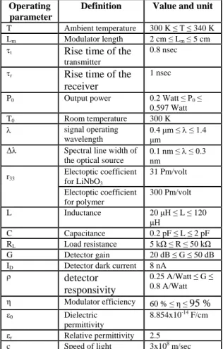
polymer electrooptic modulator devices in advanced optical communication systems over wide range of the affecting operating parameters as shown in Table 1.
Table 1: Proposed operating parameters for our suggested electrooptic modulator device.
Operating parameter
Definition Value and unit
T Ambient temperature 300 K ≤ T ≤ 340 K Lm Modulator length 2 cm ≤ Lm ≤ 5 cm
t Rise time of the
transmitter
0.8 nsec
r Rise time of the
receiver
1 nsec
P0 Output power 0.2 Watt ≤ P0 ≤
0.597 Watt T0 Room temperature 300 K
signal operating wavelength
0.4 μm ≤ ≤ 1.4 μm
Δλ Spectral line width of the optical source
0.1 nm ≤ ≤ 0.3 nm
r33
Electoptic coefficient for LiNbO3
31 Pm/volt
Electoptic coefficient for polymer
300 Pm/volt
L Inductance 20 μH ≤ L ≤ 120
μH
C Capacitance 0.2 pF ≤ L ≤ 2 pF
RL Load resistance 5 kΩ ≤ R ≤ 50 kΩ
G Detector gain 20 dB ≤ G ≤ 50 dB ID Detector dark current 8 nA
ρ detector
responsivity
0.25 A/Watt ≤ G ≤ 0.8 A/Watt
η Modulator efficiency 60 % ≤ η ≤ 95 % ε0 Dielectric
permittivity
8.854x10⁻¹⁴ F/cm
εr Relative permittivity 2.5
c Speed of light 3x10⁸ m/sec
Based on the model equations analysis, assumed set of the operating parameters, and the set of the Figs. (6-29), the following facts are assured as the following results:
i)Figs. (6, 7) have demonstrated that as the optical signal wavelength increases for both LiNbO3, and
polymer materials increases, the refractive index of both materials decreases at constant ambient temperature. But as ambient temperature increases, refractive index of polymer material decreases at constant optical signal wavelength. Moreover as ambient temperature increases, refractive index of LiNbO3 material increases at constant optical signal
wavelength .
ii)As shown in the series of Figs. (8, 9), has proved that as refractive index of LiNbO3, and polymer materials
increases, the modulator efficiency increases at constant modulator length. Moreover as modulator length based on these materials increases, the modulator length also increases.
Volume 1, Issue 7, September 2012 iv) Figs. (12, 13) have proved that modulator length
increases, inductance of lumped circuit decreases for both materials based EO modulator device at constant refractive index. Moreover refractive index increases for both materials based EO modulator device, inductance of lumped circuit also decreases at constant modulator length.
v) As shown in Figs. (14, 15), as capacitance of lumped circuit for both materials based EO modulator device increases, the 3-dB modulation bandwidth decreases at constant resistance of lumped circuit. As well as resistance of lumped circuit increases, the 3-dB modulation bandwidth decreases at constant capacitance of lumped circuit.
vi) Figs. (15, 16), as capacitance of lumped circuit for both materials based EO modulator device increases, the modulation frequency decreases at constant inductance of lumped circuit. As well as inductance of lumped circuit increases, the modulation frequency decreases at constant capacitance of lumped circuit. vii) Figs. (16, 17) have demonstrated that as optical
signal wavelength for both materials based EO modulator device increases, the transmission bit rates decrease with NRZ code at constant ambient temperature. Moreover as ambient temperature increases, the transmission bit rates decrease at constant optical signal wavelength.
viii) As shown in the series of Figs. (18, 19), as modulator length increases for both materials based EO modulator device, bit rate length product also increases at constant spectral line width of the optical source. But as spectral line width of the used optical source increases, the transmission bit rate length product decreases at constant modulator length.
ix) Figs. (20, 21) have assured that as ambient temperature increases for both materials based EO modulator device, the signal bandwidth decreases at constant modulator length. As well as modulator length increases, the signal bandwidth decreases at constant ambient temperature.
x) As shown in Figs. (22, 23), have demonstrated that as ambient temperature increases for both materials based EO modulator device, the signal bandwidth decreases at constant modulator length. As well as modulator length increases, the signal bandwidth decreases at constant ambient temperature. xi) Figs. (24, 25) have proved that as ambient
temperature increases for both materials based EO modulator device, the signal to noise ratio decreases at constant signal bandwidth. Also as signal bandwidth increases, the signal to noise ratio decreases at constant ambient temperature.
xii) As shown in the series of Figs. (26, 27) has assured that as signal to noise ratio increases, Shannon transmission bit rates also increases as constant signal bandwidth. As well as signal bandwidth increases, the Shannon transmission bit rate also increases at constant signal to noise ratio.
xiii)Figs. (26, 27) has demonstrated that as modulator length increases, Shannon product also increases as constant transmission bit rate. Moreover as transmission bit rate increases, the Shannon product also increases at constant modulator length.
VI.CONCLUSIONS
In a summary, we have showed the high speed performance of LiNbO3 and polymer materials based
electrooptic (EO) modulator in advanced optical communication systems. We have observed the increased modulator length, the increased modulator efficiency, capacitance of lumped circuit, and the decreased inductance of the lumped circuit. As well as the increased refractive index of both materials based EO modulator, the increased modulator efficiency, capacitance of lumped circuit, and the decreased inductance of the lumped circuit. It is evident that the decreased resistance, capacitance, and inductance of lumped circuit, the increased of both modulation frequency and 3-dB bandwidth. Moreover the decreased of optical signal wavelength, spectral line width of the used optical source and ambient temperature and the increased modulator length, the increased transmission bit rates and products within NRZ coding. The decreased of both modulator length, and ambient temperature, the increased signal bandwidth. Also in the same way, the decreased of both ambient temperature and signal bandwidth, the increased signal to noise ratio. The increased of both signal to noise ratio, and the signal bandwidth lead to the increased Shannon transmission bit rates and products.
REFERENCES
[1] H. V. Pham, and Y. Okamura, “Electrooptic Modulators with Controlled Frequency Responses by Using Nonperiodically Polarization Reversed Structure,” Journal of Advances in Optoelectronics, Vol. 8 , No. 1, pp. 1-8, 2008.
[2] T. Kawanishi, T. Sakamoto, and M. Izutsu, “High Speed Control of Lightwave Amplitude, Phase, and Frequency by use of Electrooptic Effect,” IEEE Journal of Selected Topics in Quantum Electronics, Vol. 13, No. 1, pp. 79– 91, 2007.
[3] H. V. Pham, H. Murata, and Y. Okamura, “Travelling Wave Electrooptic Modulators With Arbitrary Frequency Response Utilising Non Periodic Polarization Reversal,” Electronics Letters, Vol. 43, No. 24, pp. 1379–1381, 2007.
[4] H. Tazawa and W. H. Steier, “Analysis of Ring Resonator Based Traveling Wave Modulators,” IEEE Photon. Technol. Lett., Vol. 18, No. 1, pp. 211–213, 2006.
[5] G. Xu, Z. Liu, J. Ma, B. Liu, S.-T. Ho, L. Wang, P. Zhu, T. J. Marks, J. Luo, and A. K. Jen, “Organic Electrooptic Modulator Using Transparent Conducting Oxides As Electrodes,” Opt. Expr., Vol. 13, No. 3, pp. 7380–7385, 2005.
[6] S.-K. Kim, H. Zhang, D. Chang, C. Zhang, C. Wang, W. Steier, and H. Fetterman, “Electrooptic Polymer Modulators With Inverted Rib Waveguide Structures,” IEEE Trans. Microw. Theory Tech., Vol. 15, No. 2, pp. 218–220, Feb. 2003.
[7] J. Witzens, T. B. Jones, and M. Hochberg, “Design of Transmission Line Driven Slot Waveguide Mach-Zehnder Interferometers and Application to Analog Optical Links,” Optics Express., Vol. 18, No. 16, pp. 16903-16928, Aug. 2010.
Volume 1, Issue 7, September 2012 Lightwave Technology, Vol. 20, No. 10, pp.
1856-1863, 2002.
[9] H. Hu, R. Ricken, W. Sohler, and R. Wehrspohn. “Lithium Niobate Ridge Waveguides Fabricated by Wet Etching,”. IEEE Photonics Technology Letters, Vol. 19, No. 6, pp. 417-419, 2007.
[10] M. Howerton, R. Roeller, A. Greenblatt, and R. Khähenbühl, “Fully Packaged Band LiNbO3 Modulator
with Low Drive Voltage,” IEEE Photonics Technology Letters, Vol. 12, No. 7, pp. 792-794, 2000.
[11] Abd Naser A. Mohammed, M. Metawe'e, Abd El-Fattah Saad and Mohammed Tabbour, “Recent Applications of the Electrooptic Modulators in Radio Over Fiber (ROF),” Journal of Media and Communication Studies, Vol. 1, No. 6, pp. 106-115, Dec. 2009.
[12] Abd El Naser A. Mohammed, Ahmed Nabih Zaki Rashed, Gaber E. S. M. El-Abyad, and Abd-El-fattah A. Saad “Applications of Conventional and A thermal Arrayed Waveguide Grating (AWG) Module in Active and Passive Optical Networks (PONs),” International Journal of Computer Theory and Engineering (IJCTE), Vol. 1, No. 3, pp. 290-298, Aug. 2009.
[13] J. G. Nellist, Understanding Telecommunications and Lightware Systems, 2nd ed. IEEE Press, 1996.
[14] M. V. Raghavendra, P. H. Prasad, “Estimation of Optical Link Length for Multi Haul Applications,” International Journal of Engineering Science and Technology, Vol. 2, No.6, pp. 1485-1491, 2010. [15] I. P. Kaminow and T. L. Koch, Optical Fiber
Telecommunications, III, New York: Academic Press, 1997.
[16] A. Pilipetskii, “High Transmission Capacity Undersea Long Haul Communication Systems,” J. Lightwave Technol., Vol. 12, No. 4, pp. 484-496, 2006.
[17] Abd El-Naser A. Mohammed, Abd El-Fattah A. Saad, and Ahmed Nabih Zaki Rashed and Mahomud M. Eid, “Characteristics of Multi-Pumped Raman Amplifiers in Dense Wavelength Division Multiplexing (DWDM) Optical Access Networks,” IJCSNS International Journal of Computer Science and Network Security, Vol. 9, No. 2, pp. 277-284, Feb. 2009.
[18] Abd El-Naser A. Mohammed, and Ahmed Nabih Zaki Rashed, “Comparison Performance Evolution of Different Transmission Techniques With Bi-directional Distributed Raman Gain Amplification Technique in High Capacity Optical Networks,” International Journal of Physical Sciences, Vol. 5, No. 5, pp. 484-495, May 2010.
Author's Profile
Dr. Ahmed Nabih Zaki Rashed was born in Menouf city, Menoufia State, Egypt country in 23 July, 1976. Received the B.Sc., M.Sc., and Ph.D. scientific degrees in the Electronics and Electrical Communications Engineering Department from Faculty of Electronic Engineering, Menoufia University in 1999, 2005, and 2010 respectively. Currently, his job carrier is a scientific lecturer in Electronics and Electrical Communications Engineering Department, Faculty of Electronic Engineering, Menoufia university, Menouf.