Link Replicator for Fibre
Channel, Gigabit Ethernet,
HDTV and SATA
Up to 1.5 Gb/s
DescriptionThe NB4N7132 is a high performance 3.3 V Serial Link Replicator
which provides the function of serial loop replication and serial
loopback control commonly required in Fibre Channel, GbE, HDTV
and SATA applications. Other popular applications include Host Bus
Adaptors for routing between internal and external connectors, and
hot
−
pluggable links between redundant switch fabric cards.
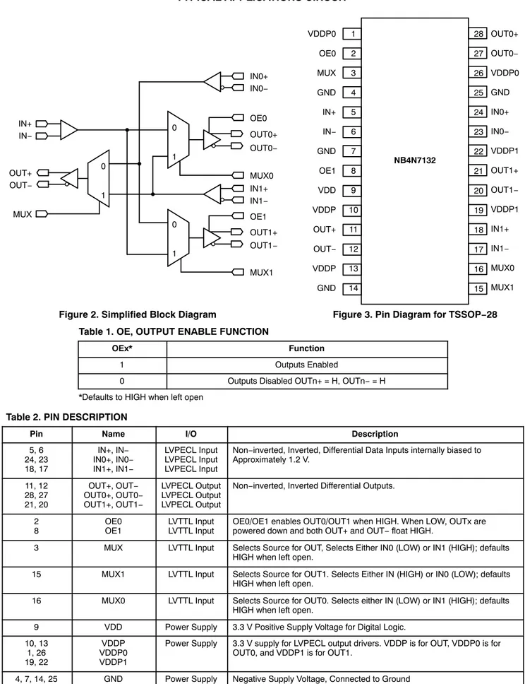
IN is sent to both OUT0 and OUT1; each output is enabled by OE0
and OE1 when HIGH. OUT0 can select either IN or IN1 via the
MUX0 pin. Likewise, OUT1 can select between IN or IN0 via the
MUX1 pin. Out can select between IN0 and IN1.
In Link Replicator applications, such as the Line Card to Switch
Card links, IN is transmitted to both OUT0 and OUT1 which either
IN0 or IN1 is selected at OUT. In Host Adapter applications, IN goes
to OUT0 (an internal connector) which returns data on IN0. IN0 is
looped to OUT1 (an external connector) which returns data on IN1
and then back to the SerDes on OUT.
The NB4N7132 is packaged in a 4.7 mm x 9.7 mm TSSOP
−
28.
Features
•
Replicates Fibre Channel, Gigabit Ethernet, HDTV, and
Serial ATA (SATA) Links
•
T11 Fibre Channel Complaint at 1.0625 Gb/s
•
No External Components Required
•
IEEE802.3z Gigabit Ethernet Compliant at 1.25 Gb/s
•
SMPTE
−
292M Compliant at 1.485 Gb/s
•
450 mW Maximum Power Dissipation
•
Operating Range: V
CC= 3.135 V to 3.465 V
•
28
−
pin, 4.4 mm x 9.7 mm TSSOP Package
•
These are Pb
−
Free Devices
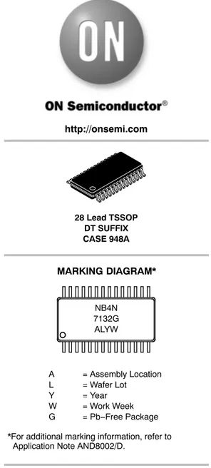
MARKING DIAGRAM*
28 Lead TSSOP DT SUFFIX CASE 948A
http://onsemi.com
*For additional marking information, refer to Application Note AND8002/D.
See detailed ordering and shipping information in the package dimensions section on page 5 of this data sheet.
ORDERING INFORMATION A = Assembly Location L = Wafer Lot Y = Year W = Work Week G = Pb−Free Package
NB4N 7132G ALYW
Figure 1. Simplified Application TX
RX
LOOP0
LOOP1 NB4N7132
http://onsemi.com
2
TYPICAL APPLICATIONS CIRCUIT
Figure 2. Simplified Block Diagram 0 1 OUT+ OUT− MUX IN+ IN− OUT1+ OUT1− MUX1 OE1 IN1+ IN1− MUX0 OUT0+ OUT0− OE0 IN0+ IN0− 0 1 0 1
Figure 3. Pin Diagram for TSSOP−28 1 2 3 4 5 6 7 8 9 10 11 12 13 14 28 27 26 25 24 23 22 21 20 19 18 17 16 15 VDDP0 OE0 MUX GND IN+ IN− GND OE1 VDD VDDP OUT+ OUT− VDDP GND OUT0+ OUT0− VDDP0 GND IN0+ IN0− VDDP1 OUT1+ OUT1− VDDP1 IN1+ IN1− MUX0 MUX1 NB4N7132
Table 1. OE, OUTPUT ENABLE FUNCTION
OEx* Function
1 Outputs Enabled
0 Outputs Disabled OUTn+ = H, OUTn− = H *Defaults to HIGH when left open
Table 2. PIN DESCRIPTION
Pin Name I/O Description
5, 6 24, 23 18, 17
IN+, IN−
IN0+, IN0−
IN1+, IN1−
LVPECL Input LVPECL Input LVPECL Input
Non−inverted, Inverted, Differential Data Inputs internally biased to Approximately 1.2 V.
11, 12 28, 27 21, 20
OUT+, OUT−
OUT0+, OUT0−
OUT1+, OUT1−
LVPECL Output LVPECL Output LVPECL Output
Non−inverted, Inverted Differential Outputs.
2
8 OE0OE1 LVTTL InputLVTTL Input OE0/OE1 enables OUT0/OUT1 when HIGH. When LOW, OUTx arepowered down and both OUT+ and OUT− float HIGH. 3 MUX LVTTL Input Selects Source for OUT, Selects Either IN0 (LOW) or IN1 (HIGH); defaults
HIGH when left open.
15 MUX1 LVTTL Input Selects Source for OUT1. Selects Either IN (HIGH) or IN0 (LOW); defaults HIGH when left open.
16 MUX0 LVTTL Input Selects Source for OUT0. Selects either IN (LOW) or IN1 (HIGH); defaults HIGH when left open.
9 VDD Power Supply 3.3 V Positive Supply Voltage for Digital Logic. 10, 13 1, 26 19, 22 VDDP VDDP0 VDDP1
Power Supply 3.3 V supply for LVPECL output drivers. VDDP is for OUT, VDDP0 is for OUT0, and VDDP1 is for OUT1.
4, 7, 14, 25 GND Power Supply Negative Supply Voltage, Connected to Ground
Table 3. ATTRIBUTES
Characteristics Value
Internal Input Pullup Resistor 96 k
ESD Protection Human Body Model
Machine Model > 100 V> 1 kV
Moisture Sensitivity (Note 1) Level 3
Flammability Rating Oxygen Index: 28 to 34 UL 94 V−0 @ 0.125 in
Transistor Count 268 Devices
Meets or exceeds JEDEC Spec EIA/JESD78 IC Latchup Test 1. For additional information, see Application Note AND8003/D.
Table 4. MAXIMUM RATINGS
Symbol Parameter Condition 1 Min Max Unit
VDD Positive Power Supply GND = 0 V 0.5 4.0 V
VINP Input Voltage, PECL GND = 0 V −0.5 VDD + 0.5 V
VINT Input Voltage, TTL GND = 0 V −0.5 VDD + 0.5 V
IOUT Output HIGH current, PECL −50 +50 mA
TC Case temperature under bias −55 +125 °C
TA Operating Temperature Range −40 +85 °C
Tstg Storage Temperature Range −65 +150 °C
JA Thermal Resistance (Junction−to−Ambient) 0 lfpm
500 lfpm TSSOP−28 7660 °C/W°C/W
JC Thermal Resistance (Junction−to−Case) (Note 2) TSSOP−28 25 °C/W
Tsol Wave Solder Pb−Free 265 °C
Stresses exceeding Maximum Ratings may damage the device. Maximum Ratings are stress ratings only. Functional operation above the Recommended Operating Conditions is not implied. Extended exposure to stresses above the Recommended Operating Conditions may affect device reliability.
http://onsemi.com
4
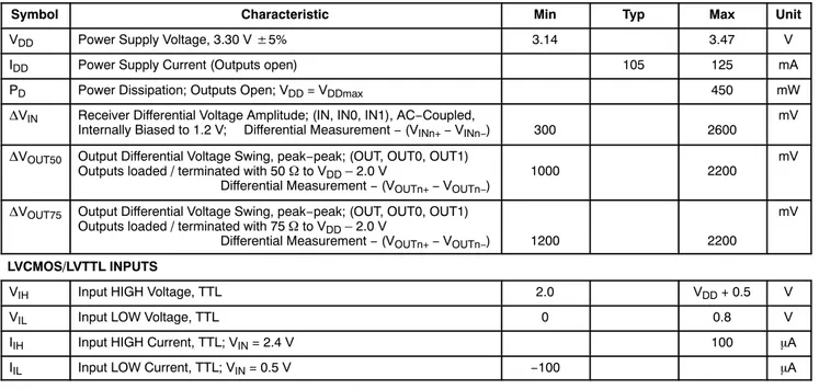
Table 5. DC CHARACTERISTICS VDD = 3.30 V $5%, GND = 0 V; TA = −40°C to +85°C
Symbol Characteristic Min Typ Max Unit
VDD Power Supply Voltage, 3.30 V $5% 3.14 3.47 V
IDD Power Supply Current (Outputs open) 105 125 mA
PD Power Dissipation; Outputs Open; VDD = VDDmax 450 mW
VIN Receiver Differential Voltage Amplitude; (IN, IN0, IN1), AC−Coupled,
Internally Biased to 1.2 V; Differential Measurement − (VINn+ − VINn−) 300 2600
mV
VOUT50 Output Differential Voltage Swing, peak−peak; (OUT, OUT0, OUT1)
Outputs loaded / terminated with 50 to VDD – 2.0 V
Differential Measurement − (VOUTn+ − VOUTn−)
1000 2200 mV
VOUT75 Output Differential Voltage Swing, peak−peak; (OUT, OUT0, OUT1)
Outputs loaded / terminated with 75 to VDD – 2.0 V
Differential Measurement − (VOUTn+ − VOUTn−) 1200 2200
mV
LVCMOS/LVTTL INPUTS
VIH Input HIGH Voltage, TTL 2.0 VDD + 0.5 V
VIL Input LOW Voltage, TTL 0 0.8 V
IIH Input HIGH Current, TTL; VIN = 2.4 V 100 A
IIL Input LOW Current, TTL; VIN = 0.5 V −100 A
NOTE: Device will meet the specifications after thermal equilibrium has been established when mounted in a test socket or printed circuit board with maintained transverse airflow greater than 500 lfpm. Electrical parameters are guaranteed only over the declared operating temperature range. Functional operation of the device exceeding these conditions is not implied. Device specification limit values are applied individually under normal operating conditions and not valid simultaneously.
Table 6. AC CHARACTERISTICS VDD = 3.3 V $5%, GND = 0 V −40°C to +85°C
Symbol Characteristic Min Typ Max Unit
fIN / OUT Input / Output Frequency Range 1.5 Gb/s
tr/tf Output rise and Fall Times (Note 3) 140 175 ps
tPD Propagation Delay, IN to OUT 0.375 4.0 ns
TDJ Deterministic Jitter Added to Serial Input Up to 1.5 Gb/s;
K28.5$ Pattern 40 ps pk−pk
NOTE: Device will meet the specifications after thermal equilibrium has been established when mounted in a test socket or printed circuit board with maintained transverse airflow greater than 500 lfpm. Electrical parameters are guaranteed only over the declared operating temperature range. Functional operation of the device exceeding these conditions is not implied. Device specification limit values are applied individually under normal operating conditions and not valid simultaneously.
3. Measured 20% to 80%
Figure 4. Timing Waveforms IN1+/−
OUT+/−
IN0+/−
IN+/−
OUT0+/−
OUT1+/−
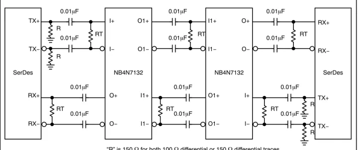
Figure 5. NB4N7132 Application Interface Example
NB4N7132 NB4N7132 SerDes
SerDes TX+
TX−
RX+
RX−
O1+
O1−
I1+
I1−
I+
I−
O+
O−
O+
O−
I+
I−
I1+
I1−
O1+
O1−
RX+
RX−
TX+
TX−
0.01F
0.01F
0.01F
0.01F
0.01F
0.01F 0.01F
0.01F 0.01F
0.01F 0.01F
0.01F R
R
RT
RT RT RT
RT RT
“R” is 150 for both 100 differential or 150 differential traces. “RT” matches the differential impedance of the link.
R
R
IN+/IN− Input Functionality
The differential inputs are internally biased to
Y
1.2 V. In
a typical application, the differential inputs are
capacitor
−
coupled and will swing symmetrically above and
below 1.2 V, preserving a 50% duty cycle to the outputs.
With this technique, the NB4N7132 will accept any
differential input allowing for LVPECL, CML, LVDS, and
HSTL input levels.
OUT+ / OUT− Outputs
The OUT+ and OUT
−
outputs of the NB4N7132 are
designed to drive differential transmission lines with
nominally 50
or 75
characteristic impedance. These
differential output buffers utilize positive emitter coupled
logic (PECL) architecture, but they do not require DC output
load resistors, and will operate properly with or without the
resistors.
OEx Output Enable
The NB4N7132 incorporates output enable pins, OE0 and
OE1, that work by powering down the output buffer and
associated driving circuitry. Using this approach results in
both differential outputs going HIGH, and a reduction in I
DDcurrent of approx. 29 mA for each disabled output pair.
When OEx is LOW, outputs are disabled, OUTx+ and
OUTx
−
are set HIGH.
Power Supply Bypass information
A clean power supply will optimize the performance of
the device. The NB4N7132 provides separate power supply
pins for the digital circuitry (V
DD) and LVPECL outputs
(VDDPn). Placing a bypass capacitor of 0.01
F to 0.1
F
on each VDD pin will help ensure a noise free V
DDpower
supply. The purpose of this design technique is to try and
isolate the high switching noise of the digital outputs from
the relatively sensitive digital core logic.
Resource Reference of Application Notes
AND8002 − Marking and Date Codes
AND8009 − ECLinPS Plus Spice I/O Model Kit
ORDERING INFORMATION
Device Package Shipping†
NB4N7132DTG TSSOP−28
(Pb−Free) 50 Units / Rail
NB4N7132DTR2G TSSOP−28
(Pb−Free) 2500 / Tape & Reel
†For information on tape and reel specifications, including part orientation and tape sizes, please refer to our Tape and Reel Packaging Specifications Brochure, BRD8011/D.
http://onsemi.com 6
PACKAGE DIMENSIONS
ÇÇÇÇÇ ÇÇÇÇÇ 0.20 A e ÇÇÇ ÇÇÇSECTION A−A
ÉÉÉ ÉÉÉ DETAIL A (L1) 0.25 15 28 14 PIN ONE LOCATION NOTES:
1. DIMENSIONS AND TOLERANCING PER ASME Y14.5M, 1994.
2. DIMENSIONS IN MILLIMETERS. 3. DIMENSION b DOES NOT INCLUDE
DAMBAR PROTRUSION. ALLOWABLE DAMBAR PROTRUSION SHALL BE 0.08 MM TOTAL IN EXCESS OF THE “b” DIMENSION AT MAXIMUM MATERIAL CONDITION.
4. DATUMS A AND B TO BE DETERMINED AT DATUM PLANE H.
B E E1 B C 1 0.10 SEATING A C D C PLANE 0.05 A A2 A1 b 28X
0.10 C B A
A A
DETAIL A
DIM MIN MAX MILLIMETERS A −−− 1.20 A1 0.05 0.15 A2 0.80 1.05 b 0.19 0.30 b1 0.19 0.25 c 0.09 0.20 c1 0.09 0.16 D 9.60 9.80 E 6.40 BSC E1 4.30 4.50
e 0.65 BSC L 0.45 0.75 L1 1.00 REF
R 0.09 −−−
R1 0.09 −−−
S 0.20 −−−
01 0 8 02 12 REF 03 12 REF__
_ _ L 03 01 R R1 S 02 H GAUGE PLANE (b) b1 c1 c 2X
28 LEAD TSSOP DT SUFFIX
CASE 948AA−01 ISSUE O
ON Semiconductor and are registered trademarks of Semiconductor Components Industries, LLC (SCILLC). SCILLC reserves the right to make changes without further notice to any products herein. SCILLC makes no warranty, representation or guarantee regarding the suitability of its products for any particular purpose, nor does SCILLC assume any liability arising out of the application or use of any product or circuit, and specifically disclaims any and all liability, including without limitation special, consequential or incidental damages. “Typical” parameters which may be provided in SCILLC data sheets and/or specifications can and do vary in different applications and actual performance may vary over time. All operating parameters, including “Typicals” must be validated for each customer application by customer’s technical experts. SCILLC does not convey any license under its patent rights nor the rights of others. SCILLC products are not designed, intended, or authorized for use as components in systems intended for surgical implant into the body, or other applications intended to support or sustain life, or for any other application in which the failure of the SCILLC product could create a situation where personal injury or death may occur. Should Buyer purchase or use SCILLC products for any such unintended or unauthorized application, Buyer shall indemnify and hold SCILLC and its officers, employees, subsidiaries, affiliates, and distributors harmless against all claims, costs, damages, and expenses, and reasonable attorney fees arising out of, directly or indirectly, any claim of personal injury or death associated with such unintended or unauthorized use, even if such claim alleges that SCILLC was negligent regarding the design or manufacture of the part. SCILLC is an Equal Opportunity/Affirmative Action Employer. This literature is subject to all applicable copyright laws and is not for resale in any manner.
PUBLICATION ORDERING INFORMATION
N. American Technical Support: 800−282−9855 Toll Free USA/Canada
Europe, Middle East and Africa Technical Support: Phone: 421 33 790 2910
Japan Customer Focus Center Phone: 81−3−5773−3850
NB4N7132/D
LITERATURE FULFILLMENT:
Literature Distribution Center for ON Semiconductor P.O. Box 5163, Denver, Colorado 80217 USA
Phone: 303−675−2175 or 800−344−3860 Toll Free USA/Canada Fax: 303−675−2176 or 800−344−3867 Toll Free USA/Canada Email: orderlit@onsemi.com
ON Semiconductor Website: www.onsemi.com Order Literature: http://www.onsemi.com/orderlit For additional information, please contact your local Sales Representative