Analysis and Design of Low Power
Arithmetic Circuits
M.Soundarya1, V.Soundharya2, K.Sowmiya3, S.Sri santhiya4 and N.Nagaraju5
UG Scholar, Department of ECE, Adhiyamaan College of Engineering, Hosur, TN, India1,2,3,4
Associate Professor, Department of ECE, Adhiyamaan College of Engineering, Hosur, TN, India5
ABSTRACT: Design of an effective circuit with low power consumption is one of the important factor for VLSI circuit designers. In this paper we are presenting a comparison and study of various arithmetic circuits, such as adder, subtractor, and multiplier. The design is implemented using modified XOR gate which is used in low power circuits. The conventional XOR gate and 6T XOR consumes difficulties in terms of area and delay, but this can be overcomed by using modified XOR design. Arithmetic circuits are used in various applications such as microprocessor, Digital Signal Processors, FIR filters, Digital Image Processing etc. The suggested circuit is better than the existing technique in terms of area and delay. The design can targated by using 180nm CMOS technology and the verification of the design can be done by using T-Spice.
KEYWORDS: EDA tool, Multiplexer, pass transistor logic, 2-T logic, multiplier, subtractor
I. INTRODUCTION
In today’s scenario, the demands of electronic devices are increasing rapidly. The use of portable electronic devices has been increased gradually. The primary requirement of portable electronic device is to reduce the power consumption and area and to increase the speed of operations. VLSI is a process where billions of transistors are embedded onto a tiny chip. The demand for the VLSI Designers is quite high for developing FPGA implementations, System on CHIP and ASIC. The Area along with minimum delay and power consumptions one of the important design consideration for the IC designers in designing portable electronic devices and hardware circuits. The dependency of power consumption is based on the number of transistors used.We have designed a 2Texor gate. By using this 2T EXOR we have designed an adder with different technique such as MUX based adder, pass transistor and 2-T logic our project is mainly depends on Gate Diffusion Input.
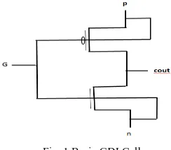
II. GDI CELL
By using GDI logic we can perform 6 operations
Table 1 Boolean function of GDI cell
N P G Out Function
0 B A AB F1
B 1 A A + B F2
1 B A A + B OR
B 0 A AB AND
C B A AB + AC MUX
0 1 A A NOT
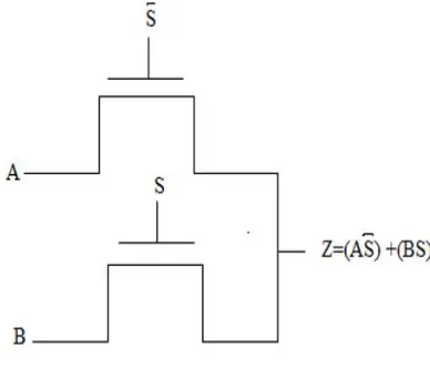
EXOR DESIGN USING GDI CELL
Comparative to other technologies GDI technology can reduce number of transistor in this EXOR design.
Fig.2 EXOR using GDI cell
MUX BASED FULL ADDER USING GDI CELL
In order to deduce the power and area, the conventional full adder [7] in reduction phase of multiplier or any other processor is replaced by a modified full adder. The modified full adder circuits consist of 2:1 MUX and XOR gate. One XOR gate in the conventional full adder is replaced by a multiplexer block so that the delay path is minimized.
DELAY = XOR + MUX
Fig 2. MUX Based Full Adder
The operation of adder is,
1. When both A and B are Zero or One, SUM = C,
2. When either of A or B is One and another is Zero, SUM = C, 3. When both A and B are Zero or One, CARRY = A,
4. When either of A or B is One and another is Zero, CARRY = C.
PASS TRANSISTOR LOGIC USING GDI CELL
In electronics, Pass transistor logic describes various logic families used in the design of integrated circuits. A pass transistor logic is used to enhance the performance of arithmetic and logic circuits. This logic can be used to reduce the count of transistors that used to make different logic gates by excluding redundant transistors. The pass transistor logic[1] used to reduce the number of transistor counts when compared to CMOS design, realizing the complex systems. When the number of transistor are decreased the chip area also decreases parallelly. When the number of transistor is reduced, we can easily decrease the number of layout elements. The pass transistor, logic design can be used to remove some transistor and it may be important to reduce the power consumption.
2-T LOGIC USING GDI CELL
The 2-T logic design [6] which is a combination of both PMOS and NMOS. This logic also known a CMOS logic. The 2-T logic is combined in a specific manner to get a full adder with SUM and CARRY as output. This logic is more efficient when compared to MUX based full adder and pass transistor logic.
Fig.4: T Logic
III. ADDER (8-BIT)
In this paper we have designed an 8-bit ripple carry adder using different logic styles such as pass transistor logic mux-based logic and 2t logic. An 8-bit ripple carry adder can be built by using 8 1-bit full adder. The Ripple carry adder [4] which creates a logic circuit using multiple full adder to add N-bit numbers.
By using above three logics we have designed a 8 bit ripple carry adder.
III. SUBTRACTOR (8-BIT)
Fig 6: Design of subtractor
IV. DESIGN OF MULTIPLIERS
First, we have designed 4x4 multiplier [3] when we obtained the logic for the modified MUX based full adder, the multiplier block is designed by combining the AND gate and the modified MUX based full adder module [8]. The AND gate is used to obtain the partial products and the modified MUX based full adder [5] is used, to sum up these products together.
Fig 8: Design of 8x8mulitplier
Fig 9: output for 8x8 multiplier
V. RESULTS AND DISCUSSION
Adders (8-bit) Number of
transistors
Delay(ns)
VI. CONCLUSION
In our project work, the 8X8 design is realized in a three different logic styles with the help of MUX based full adder, pass-transistor logic, and 2-T logic. This process of designing will not only increase the speed of the circuit but work presented in this project will achieve good results and also the demonstration of high-level optimization techniques. Simulation results show that, this proposed multiplier achieves better improvement regarding area and time delay when compared with other commonly used multiplier.
REFERENCES
[1] Y. Berg and M. Azadmehr, “Novel ultra low-voltage and high-speed CMOS pass transistor logic”, Proceedings of the IEEE Faible Tension Faible Consommation (FTFC), 2012.
[2] Hung Tien Bui, Yuke Wang and Ying Tao Jiang, “Design and Analysis of low power 10 Transistor Full Adder Using Novel XOR/XNOR gates”, IEEE Transcation on Circuits And System-II: Analog and Digital Signal Processing, vol.49,no.1, January 2002. [3] Saokar, S. S., R.M., and Siddamal, S. “High Speed Signed Multiplier for Digital Signal Processing Application”, Proc. IEEE International Conference on Signal Processing, Computing and Control (ISPCC), Waknaghat Solan, 15-17 March 2012, pp. 1-6.
[4] T.Y. Ceiang and M. J. Hsiao, “Carry-select adder using ripple carry adder Electron”, Lett, vol.34, no. 22, pp.2101-2103, 1998. [5] S. Srikanth and I. Thahirabanu, “Low Power Array Multiplier using Modified Full Adder”, 2nd IEEE International Conference on Engineering and Technology (ICETECH), 17th & 18th March 2016, Coimbatore, TN, India.
[6] N. Srinivasa Rao and B.Vijaysree, “Design the 2*1 MUX with 2T Logic and Comparing the Power Dissipation and Area with Different logics”, IJAREEIE, Vol. 4 Issue 3, March 2015.
[7] Maroju SaiKumar and Dr.P.Samundiswary,
“Design and Performance Analysis of Various Adders using Verilog”, IJCSMC, Vol.2 Issue 9, September 2013.
Multipliers (8X8bit) Number of
transistors
Delay(ns)
Mux Based Logic 1296 11.56
Pass Transistor Logic 688 10.04
2-T Logic 528 10.12
Subtractor (8-bit) Number of
transistors
Delay(ns)
Mux Based Logic 272 34.8
Pass Transistor Logic 176 33