University of Windsor University of Windsor
Scholarship at UWindsor
Scholarship at UWindsor
Electronic Theses and Dissertations Theses, Dissertations, and Major Papers
2008
A versatile, scalable, and open memory architecture in CMOS 0.18
A versatile, scalable, and open memory architecture in CMOS 0.18
μ
m
m
Karl Leboeuf
University of Windsor
Follow this and additional works at: https://scholar.uwindsor.ca/etd
Recommended Citation Recommended Citation
Leboeuf, Karl, "A versatile, scalable, and open memory architecture in CMOS 0.18 μm" (2008). Electronic Theses and Dissertations. 8251.
https://scholar.uwindsor.ca/etd/8251
Architecture in CMOS 0.l8fim
by
Karl Leboeuf
A Thesis
Submitted to the Faculty of Graduate Studies through the
Department of Electrical and Computer Engineering in Partial Fulfillment
of the Requirements for the Degree of Master of Applied Science at the
University of Windsor
1*1
Library and
Archives Canada
Published Heritage
Branch
395 Wellington Street Ottawa ON K1A0N4 Canada
Bibliotheque et
Archives Canada
Direction du
Patrimoine de I'edition
395, rue Wellington Ottawa ON K1A0N4 Canada
Your file Votre reference ISBN: 978-0-494-47093-0 Our file Notre reference ISBN: 978-0-494-47093-0
NOTICE:
The author has granted a
non-exclusive license allowing Library
and Archives Canada to reproduce,
publish, archive, preserve, conserve,
communicate to the public by
telecommunication or on the Internet,
loan, distribute and sell theses
worldwide, for commercial or
non-commercial purposes, in microform,
paper, electronic and/or any other
formats.
AVIS:
L'auteur a accorde une licence non exclusive
permettant a la Bibliotheque et Archives
Canada de reproduire, publier, archiver,
sauvegarder, conserver, transmettre au public
par telecommunication ou par Plntemet, prefer,
distribuer et vendre des theses partout dans
le monde, a des fins commerciales ou autres,
sur support microforme, papier, electronique
et/ou autres formats.
The author retains copyright
ownership and moral rights in
this thesis. Neither the thesis
nor substantial extracts from it
may be printed or otherwise
reproduced without the author's
permission.
L'auteur conserve la propriete du droit d'auteur
et des droits moraux qui protege cette these.
Ni la these ni des extraits substantiels de
celle-ci ne doivent etre imprimes ou autrement
reproduits sans son autorisation.
In compliance with the Canadian
Privacy Act some supporting
forms may have been removed
from this thesis.
Conformement a la loi canadienne
sur la protection de la vie privee,
quelques formulaires secondaires
ont ete enleves de cette these.
While these forms may be included
in the document page count,
their removal does not represent
any loss of content from the
thesis.
Bien que ces formulaires
Declaration of Originality
I hereby certify that I am the sole author of this thesis and that no part of this thesis has been published or submitted for publication.
I certify that, to the best of my knowledge, my thesis does not infringe upon anyone's copyright nor violate any proprietary rights and that any ideas, techniques, quotations, or any other material
from the work of other people included in my thesis, published or otherwise, are fully acknowledged in accordance with the standard referencing practices. Furthermore, to the extent
that I have included copyrighted material that surpasses the bounds of fair dealing within the meaning of the Canada Copyright Act, I certify that I have obtained a written permission from the
copyright owner(s) to include such material(s) in my thesis and have included copies of such copyright clearances to my appendix.
I declare that this is a true copy of my thesis, including any final revisions, as approved by my thesis committee and the Graduate Studies office, and that this thesis has not been submitted for
A lookup table is a permanent memory storate element in which every stored value corresponds to a
unique address. Range addressable lookup tables differ in that every stored value corresponds to a
range of addresses. This type of memory has important applications in a recently proposed central
processing unit which employs a multi-digit logarithmic number system that is well suited for digital signal processing applications.
Contents
Declaration of Originality iv
Abstract v
Dedication vi
Acknowledgments vii
List of Figures xiii
List of Tables xvi
List of Abbreviations xvii
1 Introduction 1
2 Background 5
2.1 Lookup Tables 5 2.1.1 Lookup Table Implementation 6
2.2 A Brief Review of Domino Logic 9 2.2.1 Static CMOS Logic 9 2.2.2 Domino Logic 11 2.2.3 Range Addressable Lookup Tables 13
3 The Range Addressable Lookup Table Architecture 15
3.1 RALUT Architecture Overview 15
3.2.2 The Address Compare Pull-Down Network 19
3.2.3 Overview of the Middle Stage 20 3.2.4 Overview of the Final Stage 20 3.2.5 Detailed Example of the RALUT Address Decoder 21
3.3 Overview of the Word Lines 24 3.4 Address and Clock Buffering Overview 24
4 Proposed VLSI Implementations in CMOS 0.18/im 25
4.1 Existing CMOS 0.35/wn Design 26 4.1.1 Selecting an Updated Technology Node 26
4.2 Design Rescaling 27 4.3 Proposed CMOS 0.18/im Implementation 28
4.3.1 Transistor Sizing for the CMOS 0.18/im Implementation 28
4.4 The High Performance CMOS 0.18/zm Implementation 28 4.4.1 High Performance CMOS 0.18/tm Implementation Design Goals 29
4.4.2 Transistor Channel Length 29
4.4.3 Keeper Widths 30 4.4.4 NMOS Chain Scaling 30 4.4.5 Transistor Widths 31 4.4.6 High Performance CMOS 0.18/im RALUT Test Circuits 31
4.4.7 High Performance Implementation Test Circuit Results and Final Transistor
Sizing 34 4.4.8 Proposed High Performance Design Layout Improvements 44
4.5 Results of the CMOS 0.18/im and High Performance CMOS 0.18/tm Designs . . . . 46
4.6 Summary 47
5 Integrated Circuit Test Platform Design 50
5.1 Test IC Overview and Testing Strategy 51
5.2 The Clock Controller Circuit 52 5.3 Internal High-Speed Clock Generation Circuit 53
CONTENTS
5.4 Test, and Output Select Circuits 58 5.4.1 Range Addressable Lookup Table Selection 61
5.4.2 Automatic Test Pattern Generator 62
5.5 The Control System 62 5.6 Hardware Synthesis 64
5.7 Simulation 64 5.7.1 Design Rule Check 66
5.8 IC Design 67 5.9 Test IC Summary and Results 67
6 Case Study: Range Addressable Lookup Tables in Artificial Neural Networks 70
6.1 Artificial Neural Networks and Activation Functions 71 6.2 A Brief Review of Different Hyperbolic Tangent Function Implementations 72
6.2.1 Piecewise Linear Approximation 72 6.2.2 Lookup Table Approximation 72
6.2.3 Hybrid Methods 73 6.3 Lookup Table Implementation of the Hyperbolic Tangent Function 74
6.4 Range Addressable Lookup Table Implementation of the Hyperbolic Tangent Function 74
6.5 Results and Comparison 75 6.6 Comparison of Different Hardware Implementations 76
6.7 Comparison to FPGA Implementations 76 6.8 Summary • 78
7 Conclusions and Future Work 79
7.1 Conclusions 79 7.2 Future Work 80
A Final Transistor Sizing 81
B Verilog Code 83
B.l Verilog Modules 83 B.l.l Automatic Test Pattern Generator 83
B.1.6 Data-out Selector 86 B.1.7 n-bit Decoder 87 B.1.8 Input Module 87 B.1.9 Memory Module 88 B.1.10 n-to-1 Multiplexer 88 B . l . l l n-wide n-to-1 Multiplexer 88 B.1.12 OK Signal Indicator 89 B.1.13 Output Controller 90 B.1.14 HDL Ralut Module 90 B.1.15 Test Circuit 91 B.1.16 Power Toggle 92 B.1.17 System Wrapper 92 B.2 Verilog Test Benches 93
B.2.1 Compare Module Test Bench 93 B.2.2 Clock Wrapper Test Bench 94 B.2.3 Controller Test Bench 96 B.2.4 OK Signal Test Bench 97 B.2.5 Test Circuit Test Bench 97 B.2.6 Power Toggle Test Bench 99
C Matlab Code 101 C.l Matlab .m Files 101
C.l.l RALUT Point Generator 101 C.l.2 Sigmoid Function 103 D Layouts for the 0.35/zm, 0.18/im, and High Performance 0.18/um Designs 104
E Synopsys Files 111
E.l Verilog .v Files I l l E . l . l Synopsys .dc Setup I l l
CONTENTS
References 113
1.1 The Hyperbolic Tangent Function 2 1.2 Lookup Table Approximation of tanh(x) with Eight Points 3
1.3 Range Addressable Lookup Table Approximation of tanh(x) with Eight Points . . . 3
2.1 Lookup Table Block Diagram 5 2.2 Lookup Table Internal Block Diagram 7
2.3 Hardware Compiler Result (a) Compared with ROM Implementation (b) 8
2.4 Schematic for a 2-Input, Static CMOS NAND Gate 10
2.5 A Domino Logic 2-Input NAND Gate 11 2.6 A Domino Logic 2-Input NAND Gate, with Keeper Transistor 12
2.7 Block Diagram of the RALUT, with n Address Bits, m Output Bits, and k Rows . . 13
2.8 RALUT (a) and LUT (b) Architectures 14 3.1 Block Diagram of the RALUT, with n Address Bits, m Output Bits, and k Rows . . 16
3.2 Block Diagram of a Five Row, Five Stage RALUT Address Decoder 17
3.3 Block Diagram of the Beginning Stage 17
3.4 Schematic of the Begin Stage 18 3.5 An Example Pull-Down Network for a 4-Bit Address Decode Stage Comparing to
"1100" 19 3.6 Block Diagram of the Middle Stage 20
LIST OF FIGURES
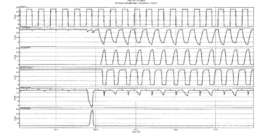
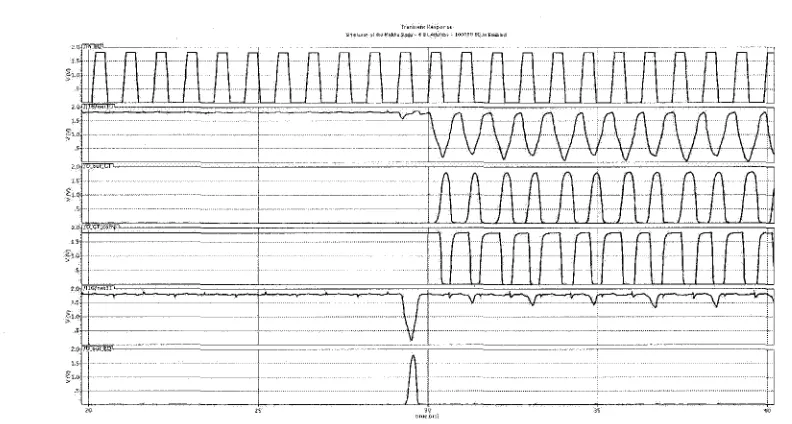
4.1 Pull-Down Networks Used in Test Circuits: (a) '1111', (b) '0000', (c) '1000' 32 4.2 Simulation Waveforms for the Beginning Address Decode Stage. From top to bottom:
clock signal, GT Critical Node, GT_out, GT_out_comp, EQ Critical Node, EQ_out . 35 4.3 Simulation Waveforms for the Middle Address Decode Stage with EQ Enabled. From
top to bottom: clock signal, GT Critical Node, GT_out, GT_out_comp, EQ Critical
Node, EQ-Out 38 4.4 Simulation Waveforms for the Middle Address Decode Stage with GT Enabled. From
top to bottom: clock signal, GT Critical Node, GT_out, GT_out_comp, EQ Critical
Node, EQ_out 38 4.5 Simulation Waveforms for the Final Address Decode Stage with EQ Enabled. From
top to bottom: clock signal, GT Critical Node, GT_out, GT_out_comp, EQ Critical
Node, EQ.out 40 4.6 Simulation Waveforms for the Final Address Decode Stage with GT Enabled. From
top to bottom: clock signal, GT Critical Node, GT_out, GT_out_comp, EQ Critical
Node, EQ-Out 40 4.7 Single-Stage Buffer Driving 8 Rows From Top to Bottom: Clock, Buffer Input, Buffer
Output, Buffer's Complemented Output, Stage's Output Signals EQ.out, GT_out,
and nGT_out_comp 43 4.8 Two-Stage Buffer Driving 8 Rows From Top to Bottom: Clock, Buffer Input, Buffer
Output, Buffer's Complemented Output, Stage's Output Signals EQ_out, GT_out,
and nGT_out_comp 43 4.9 Simulation Waveforms for the Linedriver Driving 48 Bits, From Top to Bottom: Row
1 Enable Signal, Row 1 Enable Signal Comp, Row 2 Enable Signal, Row 2 Enable
Signal Comp, Sample Output Line 44 4.10 Overlapping Wires Creating Parasitic Capacitances: (a) Original Placement, (b)
Re-duced Overlap Area, (c) Ideal Placement 47 4.11 RALUT Layout Comparison for CMOS 0.35/im design (top), CMOS 0.18/im design
(middle), and area-reduced, high-performance CMOS 0.18^m design (bottom) . . . 48
5.1 Block Diagram of the IC Subsystems 51 5.2 The Clock Selection Circuit Block Diagram 52
5.3 A 5-Stage Inverter Ring 53 5.4 Inverter Ring with Four Delay Settings 55
5.6 Inverter Ring Example Using Control Word "0010" 56
5.7 Schematic for the Switch Block 56 5.8 Transistor Schematic for the Switch Block 57
5.9 Layout for the Switch Block 57 5.10 Simulation Waveform for the Ring Oscillator @ 350 MHz 58
5.11 Simulation Waveform for the Ring Oscillator @ 200 MHz 58 5.12 Simulation Waveform for the Ring Oscillator @ 75 MHz 59
5.13 Test Circuit Block Diagram With Pipelining 60 5.14 The IC Register-Based Control System and Input Word 64
5.15 Simulation Waveforms for the RALUT, from Top to Bottom: Clock Signal, Output
Line 3, 2, 1, and 0 66 5.16 Complete IC Layout 68 5.17 Close-Up View of the IC Core 69
6.1 The Hyperbolic Tangent Activation Function 71 6.2 Piecewise Linear Approximation of tanh(x) with Five Segments 73
6.3 Lookup Table Approximation of tanh(x) with Eight Points 73 6.4 Range Addressable Lookup Table Approximation of tanh(x) with Eight Points . . . 75
A.l Beginning Stage Final Transistor Sizing 81 A.2 Middle Stage Final Transistor Sizing 82 A.3 Final Stage Final Transistor Sizing 82 D.l Begin Address Decode Stage Layouts 105 D.2 Middle Address Decode Stage Layouts 106 D.3 Final Address Decode Stage Layouts 106 D.4 Output Bits Layouts, First Row: '0', ' 1 ' Second Row: '0', 1' Third Row: '00', '01',
'10', '11' 107 D.5 Address Compare Bits From Left to Right: '0' and "1 108
List of Tables
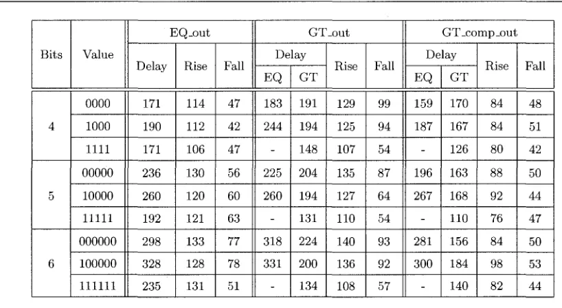
2.1 The NAND Function Input and Output Behaviour 9 4.1 Transistor Length and Width Scaling Factors 27 4.2 Beginning Stage Test Circuit Simulation Results in Picoseconds (ps) 36
4.3 Summary of Beginning Stage Worst Case Delay and Delay Per Address Bit, Results
in Picoseconds (ps) 37 4.4 Middle Stage Test Circuit Simulation Results in Picoseconds (ps) 39
4.5 Summary of Middle Stage Worst Case Delay and Delay Per Address Bit, Results in
Picoseconds (ps) 39 4.6 Final Stage Test Circuit Simulation Results 41
4.7 Summary of Final Stage Worst Case Delay and Delay Per Address Bit, Results in
Picoseconds (ps) 41 4.8 Buffer Test Circuit Results in Picoseconds (ps) 42
4.9 Output Bit Chain Length Test Circuit Simulation Results in Picoseconds (ps) . . . . 44 4.10 Area and Critical Path Delay Comparison for a 16-bit Input, 52-bit Output, 29 Row
RALUT 47 5.1 4-Bit LFSR Output States 63
5.2 Control Unit Signals 63 6.1 Complexity comparison of different implementations for 0.04 maximum error . . . . 75
6.2 Complexity comparison of different implementations for 0.02 maximum error . . . . 76 6.3 Complexity comparison of different implementations for 0.02 maximum error,
ASIC ATPG BIST CAD CMC CMOS CPU DRC DSP FET FPGA HDL IC IEEE LFSR LUT MDLNS MOSFET MSE MUX NAND NMOS PMOS RALUT RAM ROM SPICE TLNS TSMC VHDL VHSIC VLSI
Application Specific Integrated Circuit Automatic Test Pattern Generator Built-in Self Test
Computer Aided Design
Canadian Microelectronics Corporation Complimentary Metal-Oxide-Semiconductor Central Processing Unit
Design Rule Check Digital Signal Processing Field-Effect Transistor
Field Programmable Gate Array Hardware Description Language Integrated Circuit
Institute of Electrical and Electronics Engineers Linear Feedback Shift Register
Lookup Table
Multi-Dimensional Logarithmic Number System Metal-Oxide-Semiconductor Field-Effect Transistor Mean Squared Error
Multiplexer Not-AND
n-Channel MOSFET p-Channel MOSFET
Range Addressable Lookup Table Random Access Memory
Read Only Memory
Simulation Program with Integrated Circuit Emphasis Two-Digit Logarithmic Number System
Taiwan Semiconductor Manufacturing Company VHSIC Hardware Description Language
Chapter 1
Introduction
Since the first integrated circuit was successfully created in September of 1958, fabrication technology has been constantly advancing; transistors become increasingly small, allowing for faster designs at lower costs. The steady progress of miniaturization has continued almost unimpeded for fifty years until recently. As transistor sizes approach atomic sizes, numerous problems begin to arise and researchers must look elsewhere for performance improvements. Investigation into new types of digital computer architectures is one approach researchers are taking to continue to advance the state of the art of the integrated circuit.
Among these new architectures are processors which employ exotic number systems that excel in performing certain mathematical operations, such as multiplication, division and exponentiation [4], [5]. These are important operations for many digital signal processing applications, such as in a hearing aid processor, and in digital filtering [6], [15], [7]. The multi-digit logarithmic number system has recently been proposed for such purposes, and a processor employing this number system has been designed; the two-digit logarithmic number system CPU [2]. This processor is able to quickly and efficiently perform digital signal processing instructions, however it is reliant on the use of range addressable lookup tables to perform certain crucial operations, including conversion to and from binary [14].
Range addressable lookup tables, or RALUTs, function similarly to LUTs, with one key differ-ence. Every value that is stored in the RALUT corresponds to a range of input addresses. This difference allows the table size to be significantly reduced for many applications, particularly when approximating non-linear functions.
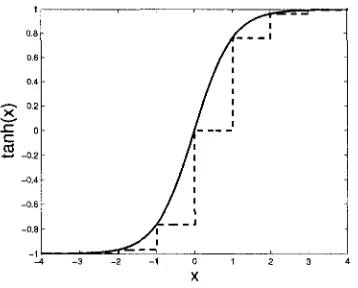
Consider, for example, the hyperbolic tangent function in Figure 1.1. It can be approximated with the use of a lookup table. The input to the lookup table is the quantized x-axis of the function, while the corresponding y-axis values are stored into the LUT, acting as outputs. Any degree of precision is possible, however more precision will require a larger table size. An example of a hyperbolic tangent function approximated by a LUT is shown in Figure 1.2. It is approximated with 8 values, and it can be seen that this is a poor approximation with very large error, particularly in the points close to the x-axis' origin. Notice that in a LUT, the stored values are evenly spaced across in input range.
X
tan
h
0.8 0.6 0.4 0.2
0 -0.2 -0.4 -0.6 -0.8
- 8 - 6 - 4 - 2 0 2 4 6 8
X
Figure 1.1: The Hyperbolic Tangent Function
1. INTRODUCTION
0.8 0.6 0.4
tanh(x
)
-0.4 -0.6 -0.8
_ i
y\
^/r i
f^ i
/ " J
_ _ J
,
« . ' I — ™"
-,
Figure 1.2: Lookup Table Approximation of tanh(x) with Eight Points
achieving a major area savings.
Figure 1.3: Range Addressable Lookup Table Approximation of tanh(x) with Eight Points The focus of this thesis is to advance the state of the art of range addressable lookup tables. To achieve this, an existing RALUT design is rescaled to use a newer fabrication process, and then further enhanced, reducing its area utilization and increasing its operating speed. A test platform is proposed to allow real-world performance data to be collected. Finally, a new application for RALUTs is proposed in the area of artificial neural networks.
C h a p t e r 2
Background
This chapter provides the reader important background information regarding lookup tables, a brief review of static CMOS, domino logic, as well as range addressable lookup tables.
2.1 L o o k u p Tables
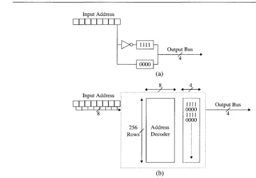
Lookup tables, or LUTs are a form of non-volatile, read-only memory. They are often used in hardware design to store functions, and are desirable in applications that require high operating speeds. As shown in Figure 2.1, LUTs have two I/O ports, an input address bus and an output bus.
Input Address
Lookup Table Output Bus
Figure 2.1: Lookup Table Block Diagram
Total Addresses = 2A d d r e s s B i t s (2.1)
The other defining parameter of the LUT, word size, is the width in bits of the output bus. Every stored word in memory is referred to by a unique address. Together, these two dimensions summarize the storage ability of the LUT, and the expression "address space x word size" will be referred to as the size of the LUT.
2.1.1 Lookup Table I m p l e m e n t a t i o n
R O M Lookup Table Implementation
Different techniques for implementing LUTs exist. One of the most common methods is ROM implementation, where the input addresses and output values are permanently stored into a hardware array. Important advantages of this approach are simplicity and predictability; given that the address space x word size parameters of the LUT remain constant, the specific words being stored into the LUT do not affect its area utilization or maximum operating speed. Additionally, it is worth mentioning that the only practical limitation of LUT size when using a ROM implementation is silicon area. These are a highly desirable qualities when designing digital systems that make use of LUTs.
One disadvantage of using a ROM array is that a proprietary tool called a "memory compiler" must be used in order to implement them in hardware. Such tools are expensive, and closed-source, meaning that the hardware designer does not have access to the internals of the ROM design. Furthermore, memory compilers are not necessarily versatile; a compiler that works for a CMOS 0.35/zm process may not function with a CMOS 90nm process.
Another problem with ROM implementation is that they consume a very large area as the number of address bits increases. Figure 2.2 shows the internal workings of the ROM implementation of the LUT. It consists of an address decoder, which scales in size with the number of input bits, and the word lines, which scale in size with the number of output bits. Thus, the total area of a ROM LUT scales approximately with Equation 2.2. As the number of input bits increases, the area utilization increases dramatically, possibly rendering the ROM implementation of LUTs impractical for very large addresses.
LUTArea a 2™ x (n + TO) (2.2)
2. BACKGROUND implementation of L U T s in m a n y different devices, including F P G A s , microcontrollers, a n d micro-processors.
n-wide m-wide Address Decoder Word Lines
•4 • •« •
Input Address n
Figure 2.2: Lookup Table Internal Block D i a g r a m
Logic Synthesizer and Logic Gate Implementation
An alternative approach to implementing L U T s is t o use a logic synthesizer, sometimes called a h a r d w a r e compiler, t o take t h e L U T ' s I / O characterisitcs, and implement it using logic gates. T h e benefit of implementing L U T s as a series of simple logic gates is t h a t there is a high probability t h a t t h e design can be simplified, yielding a large area reduction. T h e reason for this is t h a t t h e h a r d w a r e compiler carefully examines t h e specific I / O behaviour of a particular a n d "optimizes away" r e d u n d a n t logic. To d e m o n s t r a t e how a h a r d w a r e compiler can optimize a design, t h e following explanation will refer t o Figure 2.3.
Suppose a designer wanted, for whatever reason, t o create a 256 x 4 lookup table where every even address would place t h e bit p a t t e r n "1111" on t h e o u t p u t bus, and "0000" for every odd address. Given this specific design, a hardware compiler would most likely only use t h e least significant bit t o determine if t h e address were even or odd, a n d simply connect this signal t o an inverter. Referring t o Figure 2.3 p a r t (a), when t h e address is even, t h e least significant bit is ' 0 ' , a n d t h e address passes t h r o u g h an inverter and t h e first word line is enabled. Since the second word line receives t h e signal of ' 0 ' , its contents are not placed on t h e o u t p u t bus. T h e a l t e r n a t e situation occurs when an odd address is used and t h e least significant bit is ' 1 ' . This hardware compiler implementation would require (approximately) a few dozen transistors, while occupying a very tiny area, a n d o p e r a t e at very high speeds. As seen in Figure 2.3 p a r t (b), a R O M implementation would fill alternating word lines with these two p a t t e r n s , occupying the entire 256 x 4 R O M array, which is vastly more area
i 2° Rows Address Decoder
Output Bus
Input Address
1 1 1 1 1 1 1 1 1
-£>o- 1111
Output Bus
Input Address
(a) 8,
256 Rows'
Address Decoder
1111 0000 1111 0000
Output Bus
(b)
Figure 2.3: Hardware Compiler Result (a) Compared with R O M Implementation (b) t h a n t h e h a r d w a r e compiler version.
While this expample is an ideal case, it does d e m o n s t r a t e t h e capability of t h e h a r d w a r e compiler. Under most scenarios, such d r a m a t i c reductions are not possible, however area utilization is typically significantly less t h a n with R O M implementations. T h e exact area utilization and operating speed depend heavily on t h e exact bit p a t t e r n s used in t h e word lines of t h e L U T . This is a disadvantage for h a r d w a r e designers, as precise timing a n d area information are unknown until the design is synthesized, and it is possible t h a t small design changes made to t h e word lines will greatly affect these L U T a t t r i b u t e s . Another disadvantage is t h a t this approach is not feasible for very large L U T sizes. T h e processor and memory requirements of t h e logic synthesizer will increase to t h e point where a single workstation equipped with a large a m o u n t of R A M still requires days or even weeks t o determine a gate-level design for t h e L U T .
2. BACKGROUND
2.2 A Brief R e v i e w of D o m i n o Logic
Many different logic families exist for implementing logic gates; the building blocks of digital circuit design. The designs presented in this work make use of static CMOS, and domino-logic, a type of dynamic CMOS logic. The goal of this section is to provide a brief overview of these logic styles, and to impress the reader with a fundamental understanding of their mechanics, advantages, and disadvantages.
2.2.1 Static C M O S Logic
Static CMOS is a very common logic style; it is used in almost every type of design [24]. In static CMOS, a direct, low impedance path exists from the output of the gate to either VDD or VSS. PMOS transistors act as the pull-up network, while NMOS transistors form a pull-down network. When the appropriate inputs arrive at the transistors' gates, the circuit evaluates, and the output node is either connected directly to either VDD or VSS.
A Static CMOS 2-input N A N D Gate
For example, a static CMOS 2-input NAND gate is shown in Figure 2.4. It implements the function described by Table 2.2.1. The NMOS transistors connect the output directly to ground when both inputs A and B are equal to logic 1, forming the pull-down network. Similarly, when either (or both) of A or B are at logic 0, the PMOS transistors forming the pull-up network connect the output node directly to VDD.
A 0 0 1 1
B 0 1 0 1
Output 1 1 1 0
Table 2.1: The NAND Function Input and Output Behaviour
Static CMOS Properties
AHL
B H
i
Output ^
Figure 2.4: Schematic for a 2-Input, Static CMOS NAND Gate
with ease to form larger circuits. For this reason, standard cell libraries are composed of this type of logic gate.
Another important feature of static CMOS is near-zero static power consumption. Static power consumption refers to the power being consumed while the device is not switching. In other words, as long as the inputs to the logic gate remain constant, very little power is consumed. The reason why a small amount of power is still being consumed during this operating state is due to charge leakage; a physical phenomenon in which some of the charge carriers are able to "leak" through the transistor's gate oxide. This is not a major issue for fabrication processes larger than 90nm due to the relatively large oxide thickness, however when using fabrication technology at the 90nm node and beyond, this may become a greater concern.
Static CMOS gates do, on the other hand, consume switching power. This is due to the fact that when the gate's output is switching from logic 0 to logic 1, or vice-versa, both the pull-up network and pull-down network will be conducting current for a very short time interval. In other words, for a short instant (on the order of picoseconds), a short circuit from VDD to VSS is available. In addition to consuming power, this can generate noise, which may be an issue if there are analog circuits operating nearby.
2. BACKGROUND
2.2.2 Domino Logic
A dynamic logic gate is one in which the output is only valid for a short amount of time after the result is produced. [18] Athough this sounds quite restrictive, dynamic CMOS networks are useful for high-speed system design. Dynamic logic encompasses several different logic families, including domino logic.
Domino logic uses a clock signal to "precharge" a node, and later "evaluate" the node via an NMOS pull-down network. It is best illustrated via an example, as in Figure 2.5.
CLK
Figure 2.5: A Domino Logic 2-Input NAND Gate
In this schematic, when the clock signal is at logic 0, the PMOS or "precharge" transistor in this case, pulls the critical node to logic 1. This node connects to the gate of the inverter, and the output of the gate at this point is logic 0. Also notice that at this time, the NMOS transistor connected to the clock signal, the "evaluate" transistor, is not currently conducting, eliminating any path to ground that the critical node may have had.
As time elapses, the clock makes the transition to logic 1, the precharge transistor stops conduct-ing, while the evaluate transistor opens a path to ground through the NMOS pull-down network. At this point, one of two events may occur. If inputs A and B are both at logic 0, the pull-down network completes the path to ground from the critical node to the evaluate transistor, discharging the critical node, and bringing the gate output to logic 1. Alternately, if either of A or B are low, a path to ground does not exist, and the charge on the critical node remains. The gate output stays at logic 0.
power reduction is possible; there is never a short circuit from VDD to VSS as there is in static CMOS. Another advantage is the reduced area utilization made possible by only implementing the pull-down network as opposed to both pull-down and pull-up networks. For example, a 4-input NAND gate would require only two additional NMOS transistors than 2-input gate in Figure 2.5, whereas a static CMOS 4-input NAND gate would require four additional transistors: two NMOS and two PMOS.
Despite these advantages, domino logic design presents a separate set of challenges. Domino gates are sensitive to charge leakage and charge sharing, and suffer from these effects. As described in the previous section, charge leakage is the physical phenomenon in which some of the charge leaks through the transistor's gate oxide. In addition to dissipating power and creating heat, this is particularly problematic in domino gates; if the charge at the critical node dissipates too rapidly, the output will become invalid. To eliminate this concern, an additional transistor is placed between VDD and the critical node, and controlled by the gate's output, as in Figure 2.6
CLK
Figure 2.6: A Domino Logic 2-Input NAND Gate, with Keeper Transistor
This transistor is referred to as the "keeper". Its role is to maintain charge on the critical node that would otherwise bleed away over time due to charge leakage [20]. It is a very weak transistor; it is deliberately sized so that it possesses low current drive. This is done to ensure that when the circuit legitimately attempts to discharge the critical node, the keeper does not overpower the pull-down network, reducing operating speeds.
2. BACKGROUND
2.2.3 R a n g e Addressable Lookup Tables
RALUTs were originally proposed in [14] as an efficient way to implement certain non-linear, dis-continuous functions used for number conversion as well as addition and subtraction in a multi-dimensional logarithmic number system (MDLNS) [16] The MDNLS number system is able to per-form the multiplication, exponentiation, and devision operations with extreme efficiency, rendering its use extremely beneficial in certain applications such as DSP, cryptography, and multimedia processing. A primary concern of implementing a processor that employs this number system in hardware is number conversion to and from the binary number system, which is traditionally used extensively throughout most hardware designs. The conversion process is relatively time consuming unless some special hardware techniques are used. Lookup tables were proposed, however it was shown that they become very large in size as greater conversion accuracy is needed and a larger address space is required.
A block diagram showing the main components of the RALUT is shown in Figure 3.1. The architecture is divided into two main sections, the address decoder and the word lines. The input address is connected to the address decoder, and a single word line is enabled and palced on the output bus. There are only k rows, whereas in the LUT there are 2™ rows. As will be shown, the number of rows in a RALUT is not dependent on the number of bits in the input address. Finally, it is worth noting the presence of a clock signal. Although the RALUT functions like a combinational logic circuit, due to its domino logic implementation it will require a clock.
Clock Signal
Input Address j Address Decoder
Word Line Enables
-^ H
k Word Lines
RALUT Output m
Figure 2.7: Block Diagram of the RALUT, with n Address Bits, m Output Bits, and k Rows Range addressable lookup tables, or RALUTs, function very similarly to the LUTs described in the previous section. The key difference is that every stored value in a RALUT is referred to by a
range of addresses, as opposed to a single, unique address, as in Figure 2.8. As shown in the figure,
for a RALUT, every address is compared to the values stored in the address decoder. If the input address is larger than a given row, but smaller than the next, that word line is activated.
non-Input Address -n *
Address (0) Address (1) Address (2) Address (3) Address (4)
*
Data (0) Data(l) Data (2) Data (3) Data (4)
Output Bus
/ *
(a) Lookup Table Architecture
Input Address
•n *
Address (0) <= A < Address (1) Address (1) <= A < Address (2) Address (2) <= A < Address (3) Address (3) <= A < Address (4) Address (4) <= A
*
Data (0) Data(l) Data (2) Data (3) Data (4)
Output Bus
fri *
(b) Range Addressable Lookup Table Architecture
Figure 2.8: RALUT (a) and LUT (b) Architectures
linear and/or discontinuous functions. It is the RALUT's ability to span a large address space, while only using as many rows as are required that allows it to minimize area utilizaton and optimize speed. Equation 2.3 describes how the RALUT will scale in size with the design parameters n, m, and k.
C h a p t e r 3
The Range Addressable Lookup Table
Architecture
This chapter presents a detailed review of the architecture originally proposed in [14]. It begins by giving an overview of the design, and then expands on the individual components of which it is composed.
3.1 RALUT Architecture Overview
The RALUT is composed of two main parts; the address decoder, and the output rows. As shown in Figure 3.1, the RALUT uses three external signals. The n-bit wide input address and clock signal enter the address decoder portion of the architecture, which is responsible for triggering one of the
k word lines. The word lines connect to the output rows, placing an output value on the m bit wide
RALUT output bus.
3.2 The Address Decoder
RALUT Output
£
Figure 3.1: Block Diagram of the RALUT, with n Address Bits, m Output Bits, and k Rows
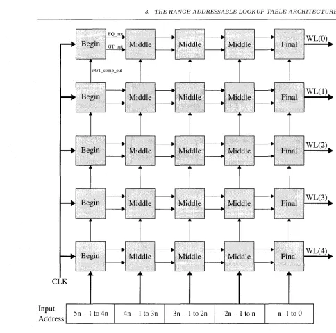
consequently the decoding array, is divided up into groups and compared in stages. This is done to minimize the length of the the domino logic NMOS pulldown network, as long NMOS chains significantly reduce circuit performance. The number of stages used depends on the width of the input address, as well as the number of bits being evaluated by each stage. A block diagram of a five row, five stage RALUT address decoder is shown in Figure 3.2. Omitted for clarity are the input address lines connecting to every row, rather than only the last row as shown in the diagram.
Figure 3.2 also shows the signals emanating from each of the stages. These are used to control the evaluation of subsequent stages. Whenever possible, subsequent stages are prevented from evaluating in order to reduce power consumption due to transistor switching. There are two ways in which this is achieved. First, the EQ_out and GT_out signals act as clock signals for subsequent stages by controlling the precharge and evaluate transistors, later evaluation stages in the same row may be disabled. If, for example, EQ_out does not make the logical transition from logic 0 to logic 1 in a given beginning stage, the subsequent stage's EQ circuit will not enter into an evaluation mode. The second technique employed to limit power consumption is the use of feedback from other rows. By having every row (except the last) use feedback from the next immediate row in the form of the nGT-Out_comp signal. If the input address is greater than the stored value in the next, higher-addressed, row, it stands to reason that the input address must be greater than the current row, and that fully evaluating this entire row is redundant. By preventing as much redundant evaluation as possible, transistor switching and thus power consumption is reduced.
It is important to note that only the first stage of the address decoder is driven by the clock. Additional stages are driven by the EQ_out and GT_out signals, which will be further explained in the example at the end of this chapter.
3.2.1 Overview of t h e Beginning Stage
A block diagram of the beginning stage is shown in Figure 3.3. Clock Signal
Input Address \ Address Decoder
Word Line Enables
3. THE RANGE ADDRESSABLE LOOKUP TABLE ARCHITECTURE CI — • — • — • — • .K Input Address Begin
EO ou^_ GT out^
nGT_comp_out
Begin
i k
Begin
i k
Begin
, k
Begin
A k
5n - 1 to 4n
Middle
i k
Middle
i i
Middle
i k
Middle
i k
Middle
A k
4n - 1 to 3n
Middle
i k
Middle
i k
Middle
i k
Middle
t k
Middle
i k
3n - 1 to 2n
Middle: i k Middle i k Middle i k Middle i k Middle
A k
2n - 1 to n
Final i k Final i k Final i k Final i k Final
A k
WL(0)^
WL(1)^
WL(2)^
WL(3)^
WL(4)^
n-1 to 0
Figure 3.2: Block Diagram of a Five Row, Five Stage RALUT Address Decoder
CLK
n Address Bits
Begin
nGT_comp_out
GT_out
EQ_out
The most significant n bits of the address are passed to every row of this stage. For every row, the beginning stage computes if the address bits being compared are greater than, or equal to its stored value. It then continues on to generate the following signals depending on how the circuit evaluated.
• EQ_out evalues to logic 1 if the input address is exactly equal to the value stored in that particular stage, and logic 0 otherwise
• GT_out evaluates to logic 1 if the input address is greater than the stage's stored value, and
logic 0 otherwise
• nGT_out_comp is simply the complement of GT_out
Note that the beginning stage is the only stage in this architecture to be driven by the clock signal. Looking closer into the beginning architecture, shown in Figure 3.4, is the transistor-level design, showing that the circuit is essentially divided into two parts; one to evaluate the EQ_out signal, and the other to evaluate the GT.out and nGT_comp_out signals.
CLK
Compare to 0
Figure 3.4: Schematic of the Begin Stage
For the beginning stage, both of these sub-circuits have a very similar, standard domino-logic gate style architecture. The only major difference is the additional inverter added after the GT_out signal to generate nGT_comp_out. When the clock is low, these circuits precharge the critical nodes A and B, meaning the outputs of this stage will be EQjj-ut = logicO, GTjout = logicO, and
nGT-comp-out — logicl during this time period. As time elapses, and the clock rises to logic 1, the
3. THE RANGE ADDRESSABLE LOOKUP TABLE ARCHITECTURE
value that this beginning stage compares to, a direct path to ground exists for node A, discharging it, bringing the output of EQ_out to logic 1. Similarly, if the input address is greater than the compare value, node B discharges, setting GT_out high and nGT_comp_out low.
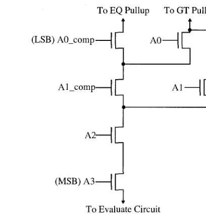
The way in which EQ and GT are evaluated depends principally on the pull-down network. In Figure 3.4, the pull-down network shows what combination of transistors are used for comparing a bit of the address to '0', and ' 1 ' (shown in green and red, respectively). The pull-down network is explained further in the next section.
3.2.2 T h e Address C o m p a r e Pull-Down Network
To EQ Pullup To GT Pullup
t
(LSB) A0_comp 1 f~ A0 1
Al_comp Al
H
A2-(MSB) A3 11 To Evaluate Circuit ^
3.2.3 Overview of t h e Middle Stage
A block diagram showing t h e input and o u t p u t signals of t h e middle stage is shown in Figure 3.6. T h e major differences between this and t h e beginning stage are t h a t this stage uses E Q J n a n d G T J n in place of t h e clock signal, and nGT_comp J n used in t h e evaluate chain.
EQ_in GT_in nGT_comp_in
n Address Bits
Figure 3.6: Block Diagram of t h e Middle Stage
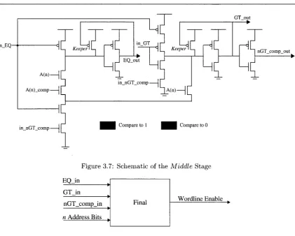
T h e schematic for t h e middle stage is shown in Figure 3.7. Once again, this stage differs only slightly from beginning. T h e E Q circuit uses in_EQ from the previous stage as a clock, a n d an ad-ditional transistor, controlled by in_nGT_comp, is added t o the evaluate p a t h . This e x t r a transistor is responsible for disabling t h e evaluate stage of t h e E Q circuit in t h e event t h a t t h e input address is greater t h a n t h e next row's value. T h e G T circuit uses b o t h t h e in_EQ a n d in_GT signals t o work t h e precharge and evaluate transistors. For this p a r t of t h e middle stage, note t h a t neither t h e E Q or G T circuits will evaluate if t h e input address is greater t h a n t h e next row due to t h e additional transistor in t h e evaluate p a t h of t h e pull-down network. Additionally, if t h e previous stage's o u t . G T signal is at logic 1, and t h e input address is not yet known t o be greater t h a n t h e next row, t h e GT_out signal of this stage will automatically propogate due to t h e additional transistors added to t h e G T circuit's parallel pull-down network. This is done t o further reduce t h e a m o u n t of switching in order t o improve power consumption.
3.2.4 Overview of t h e Final Stage
T h e final stage is shown in block diagram form in Figure 3.8. This stage makes use of E Q i n , G T J n , and nGT_comp_in, however its only o u t p u t is a word line enable signal, W L .
T h e schematic for t h e final stage is shown in Figure 3.9. This circuit is essentially t h e same as t h e middle stage, with t h e exception t h a t t h e G T and E Q subcircuits have been combined. T h e reason for this is t h a t if t h e input address is not yet known t o be greater t h a n t h e next row's c o m p a r e value, this stage must determine if it is t o be enable its row's o u t p u t word line.
Middle
3. THE RANGE ADDRESSABLE LOOKUP TABLE ARCHITECTURE
in_EQ
in_nGT_comp Compare to 1 Compare to 0
GT out
Figure 3.7: Schematic of the Middle Stage
EQ_in
GT in nGT_comp_in
n Address Bits ..
Final Wordline Enable
Figure 3.8: Block Diagram of the Final Stage
3.2.5 Detailed Example of t h e R A L U T Address Decoder
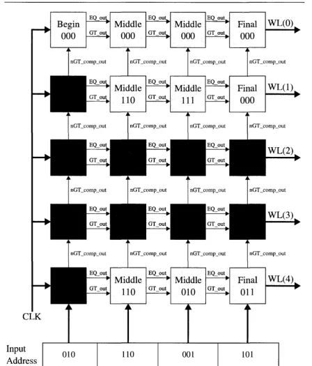
This example will refer extensively to the five row, four stage, 12-bit RALUT address decode circuit shown in Figure 3.10. Omitted for clarity are the input address lines going to every row, rather than only the last row. Also omitted are the address and clock buffers. This figure is colour coded to indicate weather a signal is logic 1 (green), logic 0, (red), and if a stage evaluates (green), or if it is disabled to save power (grey).
This RALUT address decoder can enable one of five different word line output rows, shown as WL(0) through WL(4). Evaluation begins as follows. When the CLK signal is at logic 0, the
beginning stage enters its pre-charge state. During this time, the input address may change without
affecting the RALUT's output. On the rising edge of CLK, the beginning stage of the circuit begins to evaluate.
in_nGT_comp
Compare to Compare to 0
Figure 3.9: Schematic of the Final Stage
clock signal for the next stage's EQ_out circuit. If the result is not equal however, EQ_out does not change logic levels and the next stage's EQ_out circuit remains dormant, saving power. Similarly, GT.out evaluates to logic 1 if the input address is greater than the stored value. This signal, in turn, acts as the clock for the next stage's GT.out circuit, similar to EQ_out. The last row's beginning stage's stored value is greater than the first three bits of the input address. Due to this, both the EQ.out and GT.out lines remain low, and the remainder of the final row does not evaluate, saving power.
The nGT_comp_out signal connects to the beginning stage of the previous row. This signal is simply the complement of that beginning stage's GT_out, and is used to disable the evaluation of the previous row in order to reduce power consumption. In this example, once the first three bits of the input address have been evaluated by the beginning stages, it is apparent that the first row will not require further evaluation since the input address is greater than the second row.
3. THE RANGE ADDRESSABLE LOOKUP TABLE ARCHITECTURE
CLK
Input
Address
Begin
000
EQ_out GT out
Middle
000
nGT_comp_out
EQ out„ GT out
Middle
000
nGT_comp_out
Middle
110
nGT_comp_out
EQ_out GT out
EQ_out. GT out.
Final
000
nGT_comp_out
Middle
111
nGT_comp_out
EQ_out GT out
WL(0),
nGT_comp_out
Final
000
nGT_comp_out
WL(1),
nGT_comp_out
Middle
110
010
EQ out GT out
Middle
010
EQ_out GT out
Final
011
110
001
WL(4),
101
stored value, as well as the previous stage's EQ_out and GT.out signals. Based on these, a single output word line is enabled. In this example, the input address is larger than the value stored in the third row of the address decoder, but smaller than the fourth, and the third word line is enabled. If the fourth row's final stage would have had the bit pattern 101 stored, the row would have been exactly equal to the input address, and that world line would have been enabled instead.
Once all stages have evaluated, the word line remains valid until the negative edge of the clock signal, CLK.
3.3 Overview of t h e W o r d Lines
The word lines are simple in function; given a line enable signal, they simply place the correct output bit pattern on the output bus. The line enable signal connects to a series of buffer, or line drivers, which then connect directly to NMOS and PMOS transistors which either pull-up or pull-down the RALUT output bits depending how they have been configured.
3.4 A d d r e s s a n d Clock Buffering Overview
The clock signal and input address lines must be sufficiently buffered so that as the RALUT scales in size, these signals can be driven without incident. For example, without buffering, the incoming clock signal would have to drive every beginning stage. With smaller designs this might be acceptable, however when using a design with hundreds of rows the rise and fall times of the clock signal will be very high, if the signal is able to even drive the circuit at all.
C h a p t e r 4
Proposed VLSI Implementations in
CMOS 0.18/am
This chapter discusses the design goals, methodology, and results in creating two proposed designs, both of which are in CMOS 0.18/im. The first is a rescaling of the existing 0.35/im design, in which all layout cells were recreated in the more advanced 0.18/xm node, however only two different transistor sizes were used: one for NMOS transistors, and the other for PMOS transistors. This was a very rapid approach to rescaling the design, and was used to meet a fabrication deadline for the test platform outlined in the next chapter. The second proposed design involves carefully resizing individual transistors, and further reducing area utilization to produce a high-performance RALUT. This approach proved to be much more time consuming, however simulation results prove to be optimal.
4.1 Existing CMOS 0.35/im Design
This work advances the contributions made in [14] towards a high performance, full-custom RALUT design. As such, an existing full-custom design in an CMOS 0.35/zm process existed, however many improvements could be made. The existing CMOS 0.35/xm design consisted of the following items: 1. A full-custom cell library, including beginning, middle, and final stages of the address decoder,
as well as the input and clock buffers, output bits and output linedriver cells
2. A CAD tool designed in SKILL, used in the Cadence software environment to automatically place and configure the design cells based on a user-generated file containing the desired bit patterns
While this work consists of a solid base, many improvements were possible. Originally used in 1995, CMOS 0.35/Um. is a dated technology. Many modern processors are currently designed with 90nm technology, and as of 2007 Intel has been fabricating some of their ICs using a 45nm process. Clearly, it is advantageous to advance the RALUT design to a more recent technology node, increasing its utility. In addition to porting to a more recent technology, the RALUT can be further optimized by carefully resizing its transistors. The CMOS 0.35/im design uses two different transistor sizes: one for PMOS and one for NMOS transistors. While this may greatly simplify layout design, it does not yield optimal performance.
4.1.1 Selecting an U p d a t e d Technology N o d e
The term "technology node" refers to a generation of process technology used to fabricate integrated circuit chips. The name of the node itself refers to the smallest possible transistor channel width that can be fabricated with that process. CMOS 0.18/zm, for example, allows the creation of transistors with a minimum channel width of 0.18/um. As new fabrication techniques are discovered, the creation of smaller devices is possible, enabling faster operating speeds and reduced power consumption.
Currently, several different technology nodes are available for researchers to fabricate devices, including CMOS 0.35/irn, 0.18/xm, 0.13/xm, and 90nm. When selecting which design technology to implement, and later fabricate the RALUT architecture, the following considerations were made:
• The fabrication technology design kit must be made available to the University of Windsor through CMC
4. PROPOSED VLSI IMPLEMENTATIONS IN CMOS O.l&nM
• It is preferable to use a mature design kit in which designs have been successfully fabricated in the past
• Assuming the previous criteria are met, the most recent process technology should be se-lected to ensure a high-performance design that compares well with current competing design alternatives
The University of Windsor currently has the 0.35/im, 0.18/im, 0.13/im, 90nm, and 65nm CMOS design kits, while fabrication services made available from CMC. Of these, the 0.35/im, 0.18/OTI, and 90nm kits have digital standard cell libraries. The 90nm design kit is currently considered quite "bleeding edge", and at the time of this writing, the kit is incomplete; it lacks several important elements such as timing libraries for the standard cells, which are crucial for timing-driven placement and routing. With CMOS 0.18/im and 0.35/im to choose from, 0.18/im was selected. CMOS 0.18/im was first used in 2000; it is a proven process, and significantly more recent than the 0.35/im node, which was first available in 1995.
4.2 Design Rescaling
Every fabrication technology possesses a set of design rules that, among other things, define the minimum distances that must separate certain layout elements to ensure that the integrated circuit can be fabricated. [CMC's cmospl8/cmosp35 documents] Unfortunately, the majority of these design rules do not scale simply with the technology. For example, as shown in Table 4.1, in advancing to CMOS 0.18 from CMOS 0.35, the minimum transistor widths and lengths do not scale at the same rate [26], [25]. Due to these uneven scaling factors, a full-custom layout cannot be simply rescaled when advancing to a newer technology node.
Technology Node Transistor Length
Transistor Width
CMOS 0.35/im 0.35/im 0.40/im
CMOS 0.18/im 0.18/im 0.22/im
Scaling Factor 0.51 0.55
Table 4.1: Transistor Length and Width Scaling Factors
cell must be redrawn by hand to ensure that the design rules are adhered to while maintaining a compact and efficient design.
4.3 P r o p o s e d C M O S 0.18/xra I m p l e m e n t a t i o n
The CMOS 0.18/xm implementation consists of rescaling the existing CMOS 0.35/zm design to the CMOS 0.18/xm process. All of the design cells must be redrawn and rescaled according to the CMOS 0.18/xm design rules. Similar to the CMOS 0.35/xm design, NMOS and PMOS transistors are both given a width parameter, allowing these broad categories of transistors to be easily resized. While it is not ideal to use the same size for all transistors of a particular type, it simplifies the layout, and reduces design time. It was highly desirable to fabricate an integrated circuit to test the RALUT; due to this a shortened design cycle was important, as only four months were available from the commencement of this work until the fabrication deadline.
4.3.1 Transistor Sizing for the CMOS 0.18/im Implementation
In order to determine transistor sizing for this design, a parametric analysis was performed, and the NMOS/PMOS transistor widths which provided optimal results were selected. Transistor lengths were all set to 0.18 /xm, the minimum channel length allowable for this technology node. In this case, using a PMOS width of 0.6 /zm, and an NMOS width of 0.39 /xm provided the best results. RALUT parameters such as the number of bits per address decode stage, number of output bits per linedriver, and the maximum number of rows per buffer were all configured to be the same as in the existing CMOS 0.35/xm design. Implementation results for this proposed design are shown at the end of this chapter in Section 4.5.
4.4 T h e H i g h P e r f o r m a n c e C M O S 0.18/im I m p l e m e n t a t i o n
4. PROPOSED VLSI IMPLEMENTATIONS IN CMOS 0.18piM
4.4.1 High Performance C M O S 0.18/zra I m p l e m e n t a t i o n Design Goals
Carefully sizing individual transistors should be able to increase operating speeds without dramati-cally affecting area utilization and layout complexity. The effects of proper keeper transistor sizing, and the pull-down network chain scaling should also be investigated to determine what performance gains can be made. Additionally, optimal design parameters for the maximum number of address bits per decode stage, amount of address buffering, and the number of output bits per linedriver are not known for the CMOS 0.18/xm. design. It is worthwhile to determine ideal values for these parameters to maximize performance.
To summarize, the design goals of the high performance implmentation are as follows:
1. Optimize the transistor sizing for the address decode stages, clock and address buffers, output bits, and output linedrivers
2. Determine ideal design parameters for the number of address bits per address decode stage, ideal amount of input address and clock buffering, and the maximum number of output bits per linedriver circuit
3. Report simulation performance data to serve as a guide for future hardware designers 4. Redraw cell layouts, making any possible area and performance optimizations
4.4.2 Transistor Channel Length
In digital circuit design, the transistor length, or channel length, is typically set to the minimum size allowed by the fabrication process —in this case 0.18 fi m. This is done to maximize the transistor's conduction current, which is governed by Equation 4.1 for NMOS devices and 4.2 for PMOS devices. This equation describes the transistor's maximum current drive (ID,max) m terms
of the transistor's dimensions, width (W) and length (L), a process-specific constant, the gate oxide capacitance (Cox), the gate-to-source and threshold voltages (VQS and VTH), and either the hole or
electron drift velocity, fin and nP, respectively. As shown in the equations, reducing L will increase
ID,max, resulting in, using qualitative terms, a "stronger" transistor. In short, using smaller channel
lD,max = -A«nCoa; — ( V G S ~ VTH)2 (4.1)
lD,max = yHpCox — (VGS ~ VTH) (4-2)
4.4.3 K e e p e r W i d t h s
Keeper transistors are used to minimize the effect of charge leakage. The keeper must be correctly sized to ensure that the critical node remains at logic 1 when it is charged, however it must not overpower the node if it is legitimately attempting to discharge during the evaluation phase. A keeper sizing scheme was described in [20], and was used as a starting point. To size the keeper in this way, the NMOS ^ aspect ratios in the pull-down network are summed, and multiplied by a constant less than one. This constant is then experimented with until simulation results prove optimal. For this work, the keeper was computed using this approach, and then tuned to yield optimal results. Although different keeper sizes were considered for use in the various address decode stages of the RALUT, simulation results indicated a negligeable difference. Different keeper sizes were also tested when using 4, 5, and 6 input bits per stage. Once again, operating speeds among the different keeper sizes were negligeable. Due to the minimal performance gains in sizing the keepers differently depending on the number of address bits, and among the different address decode stages, the same keeper width of 250nm was used throughout the design to simplify the layouts.
4.4.4 N M O S Chain Scaling
NMOS chain scaling is a circuit design technique employed to improve speed performance in domino logic [18]. It consists of sizing each of the transistors in the NMOS pull-down network such that the transistors closest to the critical node are smaller, while the transistors closer to the ground connection get larger. The reason for this is that when the domino logic gate enters evaluation mode, and a valid path to ground exists via the pull-down network, the charge from the transistor closest to the critical node must pass through the next transistor in the pull-down network, and the charge from both of those must past through the next, and so on. Thus the last transistor in the chain must conduct all the charge from the ones before it, and as such, modest performance increases can be expected if the chain is resized in this way.
4. PROPOSED VLSI IMPLEMENTATIONS IN CMOS 0.18^M
addition to the increased area utilization, outweighed the benefits of the increased operating speed. The final design does not make use of chain scaling for these reasons.
4.4.5 Transistor W i d t h s
With many of the transistor dimensions determined as the previous sections explained, relatively few transistor widths need to be determined. At this point it is possible to perform a parametric analysis to heuristically determine transistor sizing. This approach consists of running a simulation circuit for many different combinations of transistor widths, and selecting the best results. Many iterations are repeated, each time resizing different sets of transistors, until circuit-wide performance is maximized.
The test circuits used during these simulations are described in the following section, while results are presented at the end of this chapter.
4.4.6 High Performance C M O S 0.18/wn R A L U T Test Circuits
In order to determine the ideal transistor sizing, test circuits were developed to load each of the address decode stages appropriately, and to test performance with a variety of bit patterns.
Address Compare Bits
Each address decode stage can compare its fraction of the input address to any of 2n bit patterns,
where n is the number of bits per address decode stage. It is impractical to exhaustively test and analyze every bit pattern for every address decode stage. A more reasonable approach is to determine the worst-case bit pattern or patterns, and then to use those when evaluating performance. This is an acceptable alternative, as the most important measure of speed performance is the maximum delay, rather than the average.
Finally, when this same pattern is used, with the most significant compare bit changed to a ' 1 ' , the worst performance is usually observed. When this compare value is given an input address of all ones, every '0' transistor conducts, and all this charge must pass through the single ' 1 ' transistor along the evaluate path.
ToEQPullup ToGTPullup ToEQPullup To GT Pullup
(LSB) A0_comp 1 T A0 1 V~~ (LSB) AO 1
To EQ Pullup To GT Pullup
P (LSB) A0_comp 1 T
-C
Ht
t
(MSB) A3 1 [ To Evaluate Circuit
(a)
(LSB) A0_comp 1 T AO 1
Al_comp
A2_comp
Al
H
^
(MSB) A3_comp 1
H
S
I
H
A i _comp—| r A i —| r
A2_comp—1£ A 2_ |
^
^
To Evaluate Circuit
(b)
(MSB) A3
-To Evaluate Circuit 1
(c)
Figure 4.1: Pull-Down Networks Used in Test Circuits: (a) '1111', (b) '0000', (c) '1000'
Beginning Stage Test Circuit
In the beginning stage test circuit, a single beginning stage is attached to a set of ideal address inputs,
as well as an ideal clock signal. The stage's outputs are appropriately loaded with two middle stages, the EQ_out line attaches to the in_EQ port on the middle stage, while the nGT_comp_out of the same beginning stages connects to a second middle stage's nGT.compJn port. This was done such that the beginning stage could be simulated under typical loads.
4. PROPOSED VLSI IMPLEMENTATIONS IN CMOS O.I8/.1M
Middle Stage Test Circuit
Similar to the previous stage's test circuit, the middle stage test circuit is loaded with two additional
middle stages, and driven by ideal inputs. Two seperate simulations were run in order to determine
this stage's performance; one in which the EQ signal is changing, and the second where the GT signal is changing. This is done to determine the performance of the middle stage's delay when either of its EQ or GT subcircuits evaluate.
Final Stage Test Circuit
This test circuit is once again driven by ideal inputs, however it is loaded with two inverters connected in series to the word-line enable output. Similar to the middle stage test circuit, it is simulated in two separate runs, one using the EQ signal, the other using GT, in order to isolate and optimize the stage's delay for both subcircuits.
Buffer Test Circuit
The buffer test circuit differs from the address decode test circuits in that it is much more simple, as it only needs to drive other buffers in the buffer tree, as well as the input address lines going to the address compare bits. The following criteria had to be determined in order to achieve an optimal buffer design:
1. Buffer transistor sizing 2. Number of stages per buffer 3. Optimal buffer loading
The first of these goals is relatively easy to determine, a buffer is nothing more than an even number of inverters connected in parallel, meaning very few transistors exist. A parametric analysis quickly reveals which transistor combinations perform well. The number of stages per buffer refers to the number of inverters connected together to form the buffer. More inverters are better suited to drive larger loads, at the expense of increased area and delay. Finally, optimal buffer loading is simply the drive capability of the buffer, or in other words, the number of circuits that it can drive. As more buffers are used, the area utilization increases significantly, rendering the buffer loading parameter very important in the efficient implementation of the RALUT in hardware.
dimensional parametric analysis followed, in which the number of inverters was varied along with the buffer transistor widths. This strategy allowed the ideal transistor width and the optimal amount of loading with relative ease. Once ideal parameters were determined for a single-stage buffer, the experiment was repeated with a two-stage buffer, in order to determine its performance characteristics.
Simulation waveforms and test circuit results are presented and discussed in Section 4.4.7.
Linedriver Test Circuit
The linedriver is similar in function to the buffer, except that it is exclusively used to drive output bits and one additional linedriver stage, rather than the input address lines. The linedriver test circuit consists of two final decode stages which are configured to enable their word lines one after another as the input address increments. One of the output lines consists of all ones, or all PMOS transistors, while the second output row consists of all NMOS transistors. This is done to test the buffers with maximal loading and charge sharing. Results of this simulation, in additition to a discussion of ideal number of output bits per linedriver stage, are presented in Section 4.4.7.
4.4.7 High Performance I m p l e m e n t a t i o n Test Circuit Results a n d Final
Transistor Sizing
Simulation Environment
Currently, there are several different SPICE tools available, the most popular of which are Avanti HSPICE, Cadence Spectre, Mentor Eldo, and Silvaco SmartSpice. HSPICE and Spectre are available for use, and both were tested for use in this work. Results from each of these tools were typically within less than a perecent of each other. HSPICE typically evaluated faster, however for certain circuits, it experienced difficulty in converging to a solution. Spectre, on the other hand, performed better in this aspect, and few, if any, convergence aids were required to compute simulation results. Additionally, Spectre is better integrated with the other Cadence tools, such as Analog Environment, as they are both developed by the same company. For these reasons, Spectre was used almost exclusively throughout this work, and all of the reported results are from this netlist simulator.
Measurements