ISSN(Online): 2320-9801
ISSN (Print): 2320-9798
I
nternational
J
ournal of
I
nnovative
R
esearch in
C
omputer
and
C
ommunication
E
ngineering
(An ISO 3297: 2007 Certified Organization)
Vol. 3, Issue 7, July 2015
FPGA Implementation of Forward 2D-DCT
and Inverse 2D-DCT Based On Row-Column
Decomposition Method
Ankita Selokar
1, A.C.Kailuke
2, V.B.Bagde
3Assistant Professors, Dept. of ECE Priyadarshini Institute of Engineering & Technology, Nagpur, Maharashtra, India2,3 PG Student [E&C] , Dept. of ECE Priyadarshini Institute of Engineering & Technology, Nagpur, Maharashtra, India 1
ABSTRACT: Among various transforms, Discrete Cosine Transform i.e DCT is the most popular and effective one in both image and video compression. Two dimensional DCT takes important role in JPEG image compression. In this paper we describe the FPGA implementation of two dimensional forward Discrete Cosine Transform and inverse DCT. 2D-DCT is computed by combining two 1D-DCT that connected by a transpose buffer. Firstly we implemented the forward 1D-DCT row wise that requires addition, subtraction, registers and multipliers, and then column wise. For inverse 1D-DCT we implemented 1D-DCT column wise and then row wise. It possesses features of regularity and modularity, and is thus well suited for VLSI implementation. It can be used for the computation of either the forward or the inverse 2D DCT. Each of the sub-operation is researched for different implementations and then synthesized onto a Xilinx14.2 ISE device to be chosen for best performance.
KEYWORDS: 2D-DCT, FPGA, VHDL, image compression, video compression.
I. INTRODUCTION
The discrete cosine transform (DCT) has emerged as the most popular transform for many image/video compression applications owing to its near optimal performances. Its energy compaction efficiency is also greater then any other transform. The 2D-DCT, in particular, is one of the major operations in current image/video compression standards. It is today the most widely used orthogonal transform for applications including videophone, video conferencing and high definition television.
The 2D-DCT is computationally intensive and as such there is a great demand for high speed, high throughput and short latency computing architectures. Due to the high computation requirements, the 2D-DCT processor design has been concentrated on small non overlapping blocks (typical 8x8). Many 2D-DCT algorithms have been proposed to achieve reduction of computational complexity and thus increase the operational speed and throughput. the various algorithms and architectures for the 2D-DCT can be divided into two categories: The row-column decomposition methods and the non-row-column decomposition methods.
II. LITERATURE SURVEY
Implementation of 2D-DCT Based on FPGA with Verilog HDL- Discrete Cosine Transform is widely used in image compression.This paper describes the FPGA implementation of a two dimensional (8×8) point Discrete Cosine Transform (8×8 point 2D-DCT) processor with Verilog HDL for application of image processing. The row-column decomposition algorithm and pipelining are used to produce the high quality circuit design with the max clock frequency of 318MHz when implemented in a Xinlinx VIRTEX-ⅡPRO FPGA chip, Yunqing Ye and Shuying Cheng.
ISSN(Online): 2320-9801
ISSN (Print): 2320-9798
I
nternational
J
ournal of
I
nnovative
R
esearch in
C
omputer
and
C
ommunication
E
ngineering
(An ISO 3297: 2007 Certified Organization)
Vol. 3, Issue 7, July 2015
needs to be multiplied with post-scaler value to get the real DCT coefficients. Post-scaling process is done together with quantization process. 2D-DCT is computed by combining two 1-D DCT that connected by a transpose buffer. This design aimed to be implemented in cheap Spartan-3E XC3S500 FPGA. The 2-D DCT architecture uses 3174 gates, 1145 Slices, 21 I/O pins, and 11 multipliers of one Xilinx Spartan-3E XC3S500E FPGA and reaches an operating frequency of 84.81MHz. One input block with 8 x 8 elements of 8 bits each is processed in 2470 ns and pipeline latency is 123 clock cycles, Enas Dhuhri Kusuma, Thomas Sri Widodo.
Efficient hardware architecture for direct 2D DCT computation and its FPGA Implementation- In this paper, we propose a low complexity architecture for direct 2D-DCT computation. The architecture will transform the pixels from spatial to spectral domain with the required quality constraints of the compression standards. In our previous works we introduced a new fast 2D DCT with low computations: only 40 additions are used and no multiplications are needed. Based on that algorithm we developed in this work a new architecture to achieve the computations of the 2D DCT directly without using any transposition memory. We defined Sk functions blocks to build the 2D DCT architecture. The Sk block perform 8 function depending on the control signals of the system. The number of additions/subtractions used is 63, but no multiplication or memory transposition is needed. The architecture is suitable for usage with statistical rules to predict the zero quantized coefficients, which can considerably reduce the number of computation. We implemented the design using an FPGA Cyclone 3. The design can reach up to 244 MHz and uses 1188 logic elements, and it respect the real time video requirements, Anas Hatim, Said Belkouch, Tayeb Sadiki.III. DCT CLASSIFICATION
Direct 2-D Method:
The 2-D transforms, DCT and IDCT, to be applied directly on the N x N input data items.
Row-Column Method:
The 2-D transform can be carried out with two passes of 1-D transforms. The separability property of 2-D DCT/IDCT allows the transform to be applied on one dimension (row) then on the other (column). Requires 2N instances of N-point 1-D DCT to implement an N x N 2-D DCT.
IV. DCT ALGORITHM
In this section, the forward 1D-DCT and 1D-IDCT will be presented. For the 1x8 sequence , forward 1D-DCT can be defined as,
Where, W(0)=1
√2; W(u)=1 for u≠ 0
For inverse 1D-DCT, 𝑥 𝑖 = 2/𝑁 𝑊 𝑢 𝑋(𝑢) cos(2𝑖+1)𝑢𝜋
2𝑁
The same can be reduced to a matrix form by substituting the u values in the equations and a set of simultaneous equations in terms of input sequence x(i) and constants can be got. The same can be arranged in a matrix for to get the solution to DCT as
X = C * x For Forward DCT And x = 𝐶𝑇 * X For Inverse DCT
ISSN(Online): 2320-9801
ISSN (Print): 2320-9798
I
nternational
J
ournal of
I
nnovative
R
esearch in
C
omputer
and
C
ommunication
E
ngineering
(An ISO 3297: 2007 Certified Organization)
Vol. 3, Issue 7, July 2015
C1 = 1
2𝑐𝑜𝑠 𝜋 16, C2 =
1 2𝑐𝑜𝑠
2𝜋 16 , C3 =
1 2𝑐𝑜𝑠
3𝜋 16 , C4 =
1 2𝑐𝑜𝑠
4𝜋 16 ,
C5 = 1
2𝑐𝑜𝑠 5𝜋 16 , C6 =
1 2𝑐𝑜𝑠
6𝜋 16 , C7 =
1 2𝑐𝑜𝑠
7𝜋 16
V. FORWARD AND INVERSE DCT
Forward 2D-DCT
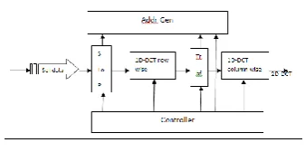
It can be introduced from the above that 2D-DCT can be decomposed into two DCT, algorithm for computing 1D-DCT can be used for 2D-1D-DCT. With row-column decomposition, the 8 point 1D-1D-DCT is applied to each row of the input 8×8 pixel matrix, and a further 1D-DCT is applied to each column of 8×8 block. The final results of 2D-DCT can be achieved by transposing the 8×8 matrix which is obtained by 8 point 1D-DCT twice. The implementation architecture of 2D-DCT is shown in Fig5.2. The 2D-DCT module includes a control module, data selection module, serial to parallel module, 1D-DCT module, parallel to parallel module, and transposing address generation module. In this paper, the 1D-DCT module is reused to meet the speed requirement and reduce hardware resource cost.
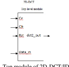
Fig 5.1. Top module of 2D-DCT/IDCT
A commonly used approach to construct 2-D DCT/IDCT is the row-column decomposition method. The decomposition performs a row-wise 1D transform followed by another column wise 1-D transform with the intermediate transposition. According to the definition of 2D-DCT,
𝑋 𝑢, 𝑣 = 𝑊 𝑢 𝑊 𝑣 2
𝑁 𝑥(𝑖, 𝑗) cos
(2𝑖 + 1)𝑢𝜋 2𝑀 cos
(2𝑖 + 1)𝑣𝜋 2𝑁
𝑁−1
𝑗 =0 𝑀−1
𝑖=0
For u = 0,1- - - - M-1 v = 0,1- - - - N-1
For W(u),W(v) =
1
√2,
1, 𝑜𝑡ℎ𝑒𝑟𝑤𝑖𝑠𝑒 for u,v = 0
Data_in:
The input pin DIN provides the data stream into the 2-D DCT core. The user can set the pin bitwidth Wdata between 8 and 24. The data is read from this port when ND is pulled high and the RFD is also set high.
CLK (Clock):
The input signal CLK is the processing clock for the fully synchronous 2-D DCT core. All internal clocking is done on the rising edge of the CLK signal.
RST (Reset):
The core offers a synchronous reset facility through this port. The input port RST allows the user to restart the 2-D DCT process. A high level on this port resets the internal state of the core. Even if a set of data has already been provided to the core, it shall not be processed. This allows the user to restart the core without actually reloading the FPGA with the design.
Dct2_out (Data output):
ISSN(Online): 2320-9801
ISSN (Print): 2320-9798
I
nternational
J
ournal of
I
nnovative
R
esearch in
C
omputer
and
C
ommunication
E
ngineering
(An ISO 3297: 2007 Certified Organization)
Vol. 3, Issue 7, July 2015
depending on the precision control selected for the results. The results of the 2-D DCT are provided sequentially on this port DOUT, column-wise.
Fig 5.2: Internal Architecture of 2D-DCT
Selection of input data is serially goes to the serial to parallel block . The transpose buffer/ parallel to parallel block operates like a temporal barrier between the first and the second 1D-DCT.
Controller:
The control module is implemented using a state machine. The state machine is divided into three states: idle state, row 1D-DCT state, and column 1D-DCT state. After the valid reset signal, the initial state is the idle state. When the valid pixel data come in, the state machine enters into row 1D-DCT state. After maintaining 64 clock cycles, it goes into column 1D-DCT state. While the column 1D-DCT state finished, the state machine recalls the idle state and sets the done signal meanwhile, then it just waits for the next 8 × 8 point 2D-DCT.
Addr_Gen module:
This module achieves the goal of transposing the semi-transformed values by controlling the read and write addresses of the memory matrix. When the state machine is in the state of row 1D-DCT, the 1D-DCT results will be written to RAM by row address mode (0,1,2,3,4,5,6,7,8,9...).When the state machine is in the state of column 1D-DCT,the data sent to the data selection module will be read from RAM by column address mode (0,8,16,24,32,40,48,56,1,9...), and the corresponding 1D-DCT results will be written to RAM by column address mode.
Inverse 2D-DCT
According to the definition of 2D-IDCT,
𝑥 𝑖, 𝑗 =2
𝑁 𝑊 𝑢 𝑊 𝑣 𝑥(𝑢, 𝑣) cos
(2𝑖 + 1)𝑢𝜋 2𝑀 cos
(2𝑖 + 1)𝑣𝜋 2𝑁
𝑁−1
𝑛=0 𝑀−1
𝑚 =0
For i = 0,1- - - - M-1 j = 0,1- - - - N-1
Fig.3 Internal Architecture Of 2D-IDCT
ISSN(Online): 2320-9801
ISSN (Print): 2320-9798
I
nternational
J
ournal of
I
nnovative
R
esearch in
C
omputer
and
C
ommunication
E
ngineering
(An ISO 3297: 2007 Certified Organization)
Vol. 3, Issue 7, July 2015
processor using two 1D DCT units. The same concept can be used for the calculation of the 2D DCT. Examining the 1D DCT equation we deduce that it necessitates totally 64 multiplications when N=8, for which the chip implementation can be hardly performed. Calculating the 1D IDCT requires the same number of operations. A commonly used approach to construct 2-D DCT/IDCT is the row-column decomposition method.
The decomposition performs a column-wise 1-D transform followed by another row wise 1-D transform with the intermediate transposition, as shown in fig.5.3 This decomposition approach has two advantages. First, the computational complexity is significantly reduced. Second, the original 1-D DCT can be easily replaced by different DCT algorithms.
The 2D-IDCT module includes a control module, data selection module, serial to parallel module, 1D-IDCT module, parallel to parallel/transposing buffer and address generation module.
Same operation is performed by 2D-IDCT as 2D-DCT.
VI. SIMULATION RESULTS Simulation Of 2D-DCT
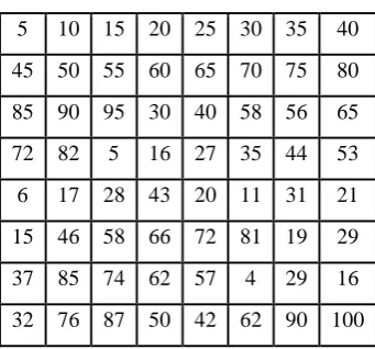
Inputs and outputs of the simulation of 2D-DCT is given in the tables below Table 6.1: Inputs To The 2D-DCT
5 10 15 20 25 30 35 40
45 50 55 60 65 70 75 80
85 90 95 30 40 58 56 65
72 82 5 16 27 35 44 53
6 17 28 43 20 11 31 21
15 46 58 66 72 81 19 29
37 85 74 62 57 4 29 16
32 76 87 50 42 62 90 100
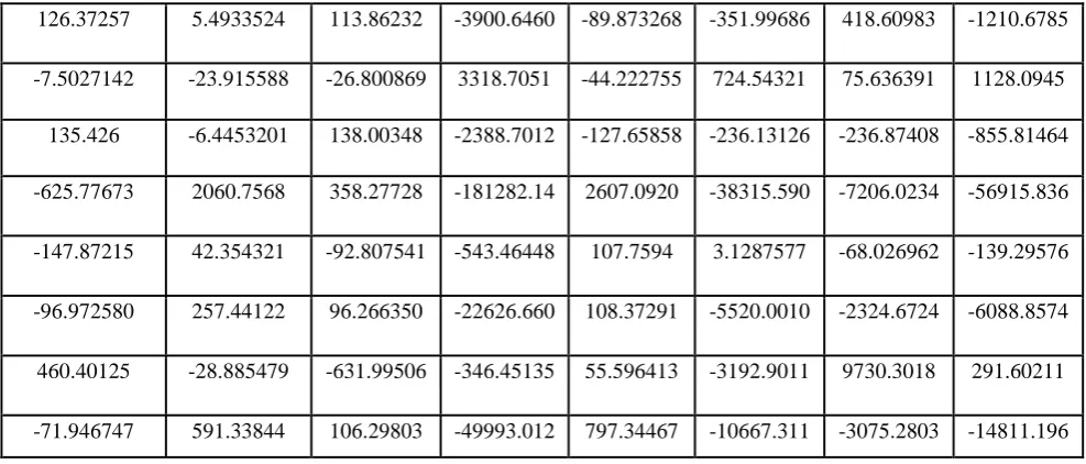
Table 6.2: Outputs Of The 2D-DCT In Decimal
126.37257 5.4933524 113.86232 -3900.6460 -89.873268 -351.99686 418.60983 -1210.6785
-7.5027142 -23.915588 -26.800869 3318.7051 -44.222755 724.54321 75.636391 1128.0945
135.426 -6.4453201 138.00348 -2388.7012 -127.65858 -236.13126 -236.87408 -855.81464
-625.77673 2060.7568 358.27728 -181282.14 2607.0920 -38315.590 -7206.0234 -56915.836
-147.87215 42.354321 -92.807541 -543.46448 107.7594 3.1287577 -68.026962 -139.29576
-96.972580 257.44122 96.266350 -22626.660 108.37291 -5520.0010 -2324.6724 -6088.8574
460.40125 -28.885479 -631.99506 -346.45135 55.596413 -3192.9011 9730.3018 291.60211
ISSN(Online): 2320-9801
ISSN (Print): 2320-9798
I
nternational
J
ournal of
I
nnovative
R
esearch in
C
omputer
and
C
ommunication
E
ngineering
(An ISO 3297: 2007 Certified Organization)
Vol. 3, Issue 7, July 2015
As shown in the above table 6.1 and table 6.2, the 8*8 matrix is given to the forward 2D-DCT block and after processing the input we will get the output 8*8 in decimal number.
Figure 6.1: Simulation Result of 2D-DCT In Decimal
Fig 6.1 simulation of 2D-DCT in which decimal/fixed number outputs are shown which is in parallel form. Firstly the data will write in the cnt_myram, then this serially data will parallely read in the next block. Now the parallel data write in to the 1D-DCT as input, this data parallel read in 1D-DCT simultaneously. Now the parallel data goes in the next memory i.e parallel to parallel and now this data will goes to the 2D-DCT and we will get the output as shown in fig 6.1
Simulation of 2D-IDCT
Inputs and outputs of the simulation of 2D-IDCT is given in the tables below Table 6.3: Inputs To The 2D-IDCT
5 10 15 20 25 30 35 40
45 50 55 60 65 70 75 80
85 90 95 30 40 58 56 65
72 82 5 16 27 35 44 53
6 17 28 43 20 11 31 21
15 46 58 66 72 81 19 29
37 85 74 62 57 4 29 16
32 76 87 50 42 62 90 100
Table 6.4: Outputs of the 2D-IDCT In Decimal
322.84485 -9365.9834
-3950.8354
-6186.6206
-14690.455
-14191.299
-5616.6934
-13558.529
-10009.693
312261.13 135256.94 200955.55 433865.06 358646.31 190633.97 453287.31
-3685.5781
102403.16 49038.477 56303.695 160540.27 188358.58 56304.074 156527.02
ISSN(Online): 2320-9801
ISSN (Print): 2320-9798
I
nternational
J
ournal of
I
nnovative
R
esearch in
C
omputer
and
C
ommunication
E
ngineering
(An ISO 3297: 2007 Certified Organization)
Vol. 3, Issue 7, July 2015
7076.2324
-12577.702
365263.84 152050.42 249694.61 587781.56 555276.88 216821.34 510137.25
-11985.000
360448.41 159832.11 217734.63 528939.75 530033.19 204757.78 523204.06
-4365.5996
133560.39 56632.617 86495.258 196980.13 180293.98 77996.734 188329.38
-10273.519
322501.56 139702.00 201517.55 448137.06 396728.50 189368.61 463569.88
As shown in the above table 6.3 and table 6.4, the 8*8 matrix is given to the 2D-IDCT block and after processing the input we will get the output 8*8 in decimal number.
Figure 6.2: Simulation Result of 2D-IDCT In Decimal
Fig 6.2 simulation of 2D-IDCT in decimal/fixed are shown which is in parallel form. Firstly the data will write in the cnt_myram, then this serially data will parallely read in the next block. Now the parallel data write in to the 1D-IDCT as input, this data parallel read in 1D-IDCT simultaneously. Now the parallel data goes in the next memory i.e parallel to parallel and now this data will goes to the 2D-IDCT and we will get the output as shown in fig 6.2
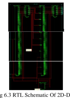
Fig 6.3 RTL Schematic Of 2D-DCT
ISSN(Online): 2320-9801
ISSN (Print): 2320-9798
I
nternational
J
ournal of
I
nnovative
R
esearch in
C
omputer
and
C
ommunication
E
ngineering
(An ISO 3297: 2007 Certified Organization)
Vol. 3, Issue 7, July 2015
VII. CONCLUSION AND FUTURE SCOPE
The 2D-DCT combined with Forward and Inverse is designed using VHDL. This has proposed a architecture based on the row column decomposition for computation of 2D-DCT. Parallel process causes latency in the system. Latency produced from this system is 113 clock cycles for 2D-DCT and 112 for 2D-IDCT. The design implemented in the Xilinx KINTEX-7 FPGA chip can complete the 2D-DCT/IDCT logic operations correctly at 161.793MHz clock frequency for forward and 141.709MHz clock frequency for inverse with the clock period of 6.181ns. Using the Row-Column decomposition algorithm, the number of calculations are logically reduced.
As we implement in this project by 8×8 block, in future we may implement it by 16×16, 32×32 upto a standard size of the image. The row column decomposition method reduces the hardware complexity as per the other methods. As the block of the size increases hardware also increases but we can implement it easily by this row column decomposition method.
REFERENCES
[1] Liu Yuejun, Su Jing and Liu Feng ,” Research on Information Hiding System based on DCT Domain”, 2010 Second International Conference on Computer Modeling and
Simulation, 978-0-7695-3941-6/10 IEEE, DOI10.1109/ICCMS.2010.342, 2010.
[2] Jie Liang and Trac D.Tran,” Fast Multiplierless Approximation of the DCT with the Lifting Scheme”, IEEE Transaction on Signal Processing ,Submitted; FEB. 2001.
[3] J. S. Chiang, Y. F. Chui and T. H. Chang. A High Throughput 2-Dimensional DCT/IDCT Architecture for Real-Time and Video System. IEEE Proc. of Int’l Conf. on Electronic Circuits and Systems, vol. 2, pp. 867 – 870, Sept. 2001.
[4] P. G. Fernández et. al. Fast RNS-Based 2D-DCT Computation on Field-Programmable Devices. IEEE Workshop on Signal Processing Systems, pp. 365 – 373, Oct. 2000.
[5] Y. T. Chang and C. L. Wang. New Systolic Array Implementation of the 2D Discrete Cosine Transform. IEEE Trans. on Circuits and Systems for Video Tech., vol. 5, no. 2, Apr. 1995.
[6] Kusuma ED, Widodo TS “FPGA implementation of pipelined 2D-DCT and quantization architecture for JPEG image compression”. Intern Symp Inform Tech (ITSim) pp 1-6,2010.
[7] A. Hatim, S. Belkouch “Efficient hardware architecture for direct 2D DCT computation and its FPGA Implementation”.-2013
[8] Yunqing Ye, Shuying Cheng “Implementation of 2D-DCT Based on FPGA with Verilog HDL”. Electronics and Signal Processing, LNEE 97 , pp.633-639.
[9] Sun, C.C., Ruan, S.J., Heyne, B., Goetze, J.: Low-power and high-quality Cordic-based Loeffler DCT for signal processing. IET Circuits Devices Syst. 1(6), 453-461 (2007).
[10] Khayatzadeh, A., Shahhoseini, H.S., Naderi, M.:Systolic Cordic Dct:An Effective Processing and its Applications, vol.2, pp. 193-196(2003).
BIOGRAPHY
Ankita Selokar is a student in the Electronics & Communication Department, Priyadarshini Institute of Engineering & Technology, R.T.M.Nagpur University. She received B.E (Electronics) degree in 2013 from DBACER, Nagpur, MS, India.