One Bit-Line Multi-Threshold SRAM Cell
With High Read Stability
Prangya Parimita Nanda
1, Kanan Bala Ray
2, Sushree Sangita Das
3PG Student, School of Electronics Engineering, KIIT University, Bhubaneswar, Odisha, India1
Asst. Prof., School of Electronics Engineering, KIIT University, Bhubaneswar, Odisha, India2
PG Student, School of Electronics Engineering, KIIT University, Bhubaneswar, Odisha, India3
ABSTRACT: Memory are inherent part of the nearly all of the digital models and so minimization of power usage of a memory is major role in upgrading the system efficiency, performance reliability. In the paper new multi-threshold one bit-line SRAM cell is proposed , for both read and write operation one bit-line is used. Minimization of power usage because of one bit-line usage and more read stability than conventional multi threshold SRAM cell. In between the proposed multi-threshold one bit-line SRAM cell and conventional multi-threshold SRAM cell comparison will be held in terms of power usage, SNM, delay. The proposed multi-threshold one bit-line SRAM cell usage 94.6% reduction in power in write 1 operation, 93.1% reduction in power in read 1 operation than multi-threshold SRAM.
We drawn the schematics using virtuoso ADE of cadence ,and all simulation data are taken out using cadence spectre analyzer with 45nm technology library at 1.8v.
KEYWORDS: One bit-line, Multi-threshold SRAM cell, less power ,Read stability , SRAM(static random access memory), SNM(static noise margin)
I. INTRODUCTION
All manuscripts In modern electronics SRAM has grow to be an integral part of high speed memory as the demand of high performance and high stability in deep sub-micron cmos design is gradually increasing. In SRAM cells, we facing several challenges like power consumption problems, stability and area due to device scaling. Considerable problems have already been experienced when the sleepy multi-threshold SRAM cell is used. multi-threshold SRAM cell gives low stability. During read operation, voltage is divided in between the pass and storage cell transistors, so
stability decreases. since conventional multi-threshold SRAM cells is work on delicately balance transistors and cell
gives low stability during read operation[1].
A. multi-threshold SRAM
The circuit diagram of multi threshold SRAM is given in figure.1.
Figure 1. Multi Threshold Voltage Circuit Approach
II. PRPOSED ONE BIT-LINE MULTI-THRESHOLD SRAM CELL
Main motive of proposing this one bit line multi threshold SRAM cell having good read stability and SNMs . Proposed one bit line multi threshold SRAM cell consists of six low threshold transistors and four high threshold transistors , one bit-line , a word line and a read-line Two pairs of Sleep transistors are used . One in each pair is activated during idle mode based upon the value of the bit stored in the cell. This disconnects the OFF transistors from supply while retaining supply to the ON transistors. Whereas three lines are required for conventional multi-threshold SRAM cell i.e. Two complementary bit-line (BL and BL') and a word line ,so one bit-line consuming more power as compare to conventional multi-threshold SRAM cell.
The circuit diagram of one bit-line multi-threshold SRAM cell is shown in figure 2.
A. Memory cell operation-
Hold operation-
When the stored data of the cell is 1 i.e. Qm=VDD & Qm'=0, then the two memory nodes will work as a loop at their respective voltages. Though the stored data of the cell is 0(Qm=0, Qm'=VDD) ,Qm is afloat. Leakage current in M2 transistor have to be less than leakage current in M5 transistor to guaranty Qm is in state of logic low. This condition is satisfied because current driver of PMOS(M5) is lesser than NMOS(M2).
Write operation-
In case of writing, the demanded data to be written will be given on bit-line & after that word line (WL) will be operated .For overpower the cell Strong pass transistor permits bit-line. For write 1 operation, bit-line should be in logic high i.e. VDD. For write 0 operation, bit-line should be in the state of logic '0' and then after word line have to be charged to VDD.
Read operation-
To read the stored data from the cell, firstly bit-line rises to logic '1'. RL is active after the bit-line rises to VDD. When the bit-line is discharging or holding the stored charge ,then we can determine the stored data of one bit-line multi-threshold SRAM cell . If bit-line goes low after rises the read-line to VDD, It shows one bit-line multi-threshold SRAM cell stored the value '0' in it. If bit-line is holding the stored charge then in one bit-line multi-threshold SRAM cell is storing the value'1'.
Consider that one bit-line multi-threshold SRAM cell is firstly stored a value '0' (Qm=0,Qm'=1). When bit-line rises to VDD and RL is asserted to VDD , MRA1 ,M7 and MRD1 transistors are on because RL is at logic high. Now bit-line has way to drain the charges to ground through MRA1 ,M7 and MRD1 transistors . So falls down to logic '0' showing stored data is '0'. Consider that one bit-line multi-threshold SRAM cell is firstly stored a value '1' (Qm=1, Qm'=0)when bit-line is rises to VDD and RL is asserted to VDD , MRA1 and M7 is off and MRD1 is on. MRD1 is on because read line is in VDD. MRA1 and M7 is off because Qm'=0. Now BL has no way to drain the charges to ground hence it read a '1'.
III. SIMULATION RESULTS
For SNM and power consumption of the proposed one bit-line multi-threshold SRAM cell, simulation is occurred at 1.8v through sepectre simulator using the cadence gpdk 45nm technology. supply voltage in the proposed circuit is 1.8v.
A. Total power calculation:
Total power used by SRAM cell is equal to summation of the power calculated from main supply voltage source, bit-line voltage sources, read-line voltage sources . multiplying the average current source and source ,we can calculate power usage at that source[6].
Table 1: Percentage power improvement in the Multi VTH SRAM using one bit-line compared to the Multi
VTH SRAM cell
Operation WRITE 1 READ 1 Multi-threshold SRAM cell 62.6uW 192.2uW
One bit-line multi-threshold SRAM cell 3.357uW 13.22uW
B. Delay calculation-
In SRAM cell, delays are total time taking to reading or writing a value from the SRAM cell. The time variation in between 10% and 90% of the voltage swing, the delay is measured.
Table 3: Delays of Multi VTH SRAM using one bit-line and Multi VTH SRAM cell
Operation WRITE 1 READ 1 Multi-threshold SRAM cell 5.331ps 5.2205ps
One bit-line multi-threshold SRAM cell 1.3315ps 1.4256ps
C.STATIC NOISE MARGIN(SNM)-
SNM is defined as "the maximum amount of noise voltage that can be introduced at the output of the two inverters, such that cell retains its data"[7][8][3].
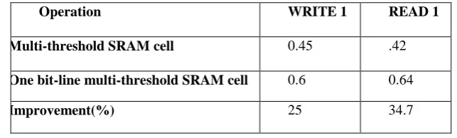
Table 4: Percentage SNM improvement in the Multi VTH SRAM using one bit-line compared to the Multi
VTH SRAM cell
Operation WRITE 1 READ 1 Multi-threshold SRAM cell 0.45 .42
One bit-line multi-threshold SRAM cell 0.6 0.64
Improvement(%) 25 34.7
IV. CONCLUSION
With the goal of low power ,less delay and better SNM in SRAM cell, this one bit-line multi-threshold SRAM is proposed. The one bit-line multi-threshold SRAM usage 94.6% reduction in power in write 1 operation, 93.1% reduction in power in read 1 operation than multi-threshold SRAM. The above circuit is proposed and simulated in cadence virtuoso environment in 45nM technology.
REFERENCES
1. Kaushik Roy, Saibal Mukhopadhyay, Hamid Mahmoodi-Meimand, "Leakage CurrentMechanisms and Leakage Reduction Techniques in Deep-Submicro meter CMOS Circuits",Proceedings Of The IEEE, Vol. 91, No. 2, February 2003.
2. S.Lakshmi Narayan, Reeba Korah and N.Krishna Kumar," A Novel Sleepy Stack 6-T SRAM Cell Design for Reducing Leakage Power in Submicron Technologies", International conference on Communication and Signal Processing, IEEE, April 3-5, 2013,India.
3. S. K. Singh, S. V. Singh, B. K. Kausik C. Chauhan, T. Tripathi," Characterization & Improvement of SNM in Deep Submicron SRAM Design",978-1-4799-2866-8/14/$31.00 ©2014 IEEE.
4. Kaushik Roy, Hamid Mahmoodi-Meimand, and Saibal Mukhopadhyay," Leakage Control for Deep-Submicron Circuits",IEEE.
5. B. Dilip,P. Surya Pras Ad & R. S. G. Bhavani," Leakage Power Reduction In Cmos Circuits Using Leakage Control Transistor Technique In Nanoscale Technology",Ijess,Issn: 2231- 5969, Vol-2 Iss-1, 2012.
6. Saurabh, S. Shekhar, A. Purwar and S. Biswas," New Improved Low Power and High SNM One Metal SRAM in 32 nm Technology",2014 International Conference on Computer Communication and Informatics (ICCCI -2014), Jan. 03 – 05, 2014, Coimbatore, INDIA, 978-1-4799-2352-6/14/$31.00 ©2014 IEEE.
8. Koichi Takeda, Yasuhiko Hagihara, Yoshiharu Aimoto, Masahiro Nomura, Yoetsu Nakazawa, Toshio Ishii, and Hiroyuki Kobatake, “A Read-Static Noise-Margin-Free SRAM Cell for Low-VDD and High-Speed Applications,” 0018-9200 2006 IEEE.
BIOGRAPHY
Prangya Parimita Nanda is a PG student of VLSI Design & Embedded System in the Electronics Department, School of Electronics Engineering, KIIT University. She received Bachelor of Technology (BTech) degree in 2013 from SIET, Dhenkanal, Odisha, India. Her research interests are low power VLSI design, memory design etc.
Kanan Bala Ray is an Asst. Prof. in the Electronics Department, School of Electronics Engineering, KIIT University. She is perusing Ph.D from KIIT University. She received Master of Technology (MTech) degree from KIIT University, Odisha, India. Her research interests are low power VLSI design, memory design etc.