ISSN(Online): 2320-9801
ISSN (Print): 2320-9798
I
nternational
J
ournal of
I
nnovative
R
esearch in
C
omputer
and
C
ommunication
E
ngineering
(An ISO 3297: 2007 Certified Organization)
Vol. 3, Issue 9, September 2015
Design and Implementation of Low Cost Area
Efficient ZTCAM
Lincy Syril
M. Tech Scholar (VLSI & Embedded Systems), Dept. of ECE, IIET, M.G. University, Kottayam, Kerala, India
ABSTRACT: The demand for memory has been increased tremendously day by day. The searching operation of data in memory and area are the main problem that are faced by the user. It increases power consumption, cost and access time. The SRAM based architecture of TCAM known as ZTCAM is a special type of memory, which receives an input search word and returns the address of that word which it is stored on its data bank. ZTCAM logically divides the classical TCAM table along columns and rows into hybrid TCAM sub tables and then maps them to their corresponding memory blocks. During search operation, the memory blocks are accessed by their corresponding sub
words of the input word and a match address is produced. When compared to RAM, Ternary Content Addressable
Memories (TCAMs) suffer from certain limitations such as low storage density, relatively slow access time, low
scalability, complex circuitry, andhigher cost. So this paper proposes a low cost and an area efficient novel architecture
for SRAM based TCAM known as ZTCAM which emulates the functionality of TCAM. The design is equipped with clock gating scheme so that efficient power management is achieved. The architecture was verified by VHDL.
KEYWORDS: Linear Priority Encoder; hybrid partitioning; clock gating; Ternary Content Addressable Memory (TCAM); Static Random Access Memory (SRAM)
I. INTRODUCTION
Ternary Content Addressable Memory (TCAM) is an outgrowth of Random Access Memory (RAM) but provides access to stored data by contents rather than by an address and outputs the match address unlike RAM. Since TCAM can store don’t care state(x), which can be matched to both 0 and 1 during a comparison operation, multiple matches may occur. A typical CAM compares search key with all the stored words in parallel and returns the address of the best match. Since TCAM provides high speed parallel search operation, it has a wide applications such as in network routers, translation look-aside buffers in microprocessors, data compression, real-time pattern matching in virus-detection, gene pattern searching in bioinformatics, and image processing.
This paper presents a memory architecture, named area efficient ZTCAM which uses hybrid partitioning of TCAM table to achieve the TCAM functionality. The proposed ZTCAM may be used in networking systems where many data need to be compared in parallel at high speed. At present, TCAMs are used in networking systems but are expensive and not scalable with respect to clock rate or circuit area compared with SRAMs.
In this work, memory mapping is done to make the architecture of ZTCAM more area efficient. This has reduced the area of the architecture without affecting the processing time and the delay. The concept of clock gating also added to the design to achieve efficient management of power.
II. RELATED WORK
ISSN(Online): 2320-9801
ISSN (Print): 2320-9798
I
nternational
J
ournal of
I
nnovative
R
esearch in
C
omputer
and
C
ommunication
E
ngineering
(An ISO 3297: 2007 Certified Organization)
Vol. 3, Issue 9, September 2015
record distribution and how these records are accessed. If many records have been placed in an overflow area due to collisions, a lookup may not finish until many buckets are searched. When stored keys contain don’t care bits in the bit positions used for hashing, then to maintain the significance of don’t care bits, such keys must be duplicated in multiple buckets, leading to an increased memory requirement. On the other hand, if the search key contains don’t care bits which are taken by the hash function, then multiple buckets must be accessed that results in performance degradation. The purpose of TCAM is that it provides a deterministic search performance but hash-based CAMs do not provide deterministic performance because of potential collisions and are inefficient in handling wild-card [18].The performance of the methods in [5,9] greatly depends on hash function. Hash function that minimizes the probability of collision is considered good. However, for random data, which hash function is better cannot be known in advance [19]. SRAM-based pipelined CAMs also take multiple clock cycles to accomplish a search operation and the memory utilization is also not efficient [10]. In RAM based associative CAM devices [6] presented, has some unavoidable disadvantages. The size of memory depends on number of bits in the TCAM word. Size increases exponentially with the increase in the number of bits in the TCAM word. For instance, 36 bits word needs a 64 GB of RAM. Such a huge memory results in increased area, cost, and power consumption.Thus, making the method practically infeasible for an
arbitrarily large bit pattern. Circuits to generate sequential index [7] claims that a CAM of size up to 2𝑤-words × w bit
can be emulated with 2𝑤memory bits. If CAM is of size 2𝑤×wbits, then it implies that the number of addresses and
the total possible combinations of wbits are same. For example, for 4 bits word, the total combinations are 24 = 16, and
to store 24CAM words, 24 addresses are required. Thus, 24 bits are needed to emulate the CAM functionally with
RAM, where each TCAM word is mapped to its corresponding memory bit. In addition, entries in TCAM table must be in ascending order and are then mapped to their corresponding memory bits. During the ascending arrangement, how the method takes care of the original address order is not mentioned. However, if original addresses are considered, memory and power requirements further increase. The method does not talk about the storage of original addresses and partitioning scheme. In memory and power efficient mechanism for fast table lookup [7] is not completely RAM-based structure and uses classical CAM as a part of the overall structure. Thus, the combination of small part of CAM and large part of RAM provides overall memory structure. Therefore, this scheme inherits the inborn disadvantages of CAM technology. The partitioning scheme of this method is also very difficult and time consuming. Conventional TCAM table is divided into groups using some distinguishing bits in TCAM entries in such a way that only one entry in each group can possibly match any given input. In typical TCAM applications, data are totally random, which
implies that finding distinguishing bits in CAM entries and then making partitions would be very time consuming.In
paper[1], TCAM is designed using SRAM which is called as Z-TCAM , perform hybrid partitioning of the conventional TCAM table. Hybrid partitioning is the combination of vertical and horizontal partitioning. Vertical partitioning means column-wise partitioning and horizontal partitioning means row-wise partitioning of TCAM Table. Even though the TCAM table provides look up of entire table in single clock it has various disadvantages. TCAM cells, comparator’s circuitry adds complexity to the architecture.
III. PROPOSED ARCHITECTURE OF ZTCAM
A. Overall Architecture:
Fig. 1illustrates the overall architecture of ZTCAM, where each layer represents the architecture depicted in Fig. 2.
ZTCAM has L number of layers and a CAM priority encoder (CPE). As can be seen from Fig.1, N subwords are simultaneously received by all the L layers during the lookup operation. Each layer outputs a potential match address (PMA). The PMAs are given to CPE, which selects match address (MA) among PMAs. For instance, if the proposed TCAM produces PMAs from layers 4, 5, 7, and 10 for an arbitrary input word, CPE selects PMA from
layer 4 as MA, considering it has the highest priority. The overall architecture of TCAM is built by hybrid
ISSN(Online): 2320-9801
ISSN (Print): 2320-9798
I
nternational
J
ournal of
I
nnovative
R
esearch in
C
omputer
and
C
ommunication
E
ngineering
(An ISO 3297: 2007 Certified Organization)
Vol. 3, Issue 9, September 2015
Table 1 .TCAM Table and Its Hybrid Parameters
Fig.1. Overall Architecture of ZTCAM
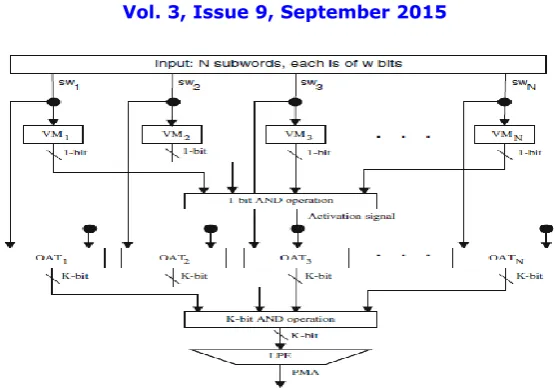
B. Area Efficient Layer Architecture Of ZTCAM
Fig.2 depicts the layer architecture of ZTCAM. Since the total number of vertical partitions is N in a layer, to
accommodate data in N vertical partitions, N validation memories (VMs) and Noriginal address tables (OATs) are
required. To achieve the TCAM functionality, the layer architecture is also equipped with 1-bit AND operation,K-bit AND operation, and a Layer Priority Encoder (LPE). Each hybrid partition in a layer has its corresponding VM and
OAT. For instance, HP11 has its correspondingVM11and OAT11. The VM and OAT of its corresponding partition
constitute a pair. Thus, for N partitions ,N pairs are required; each for a hybrid partition in a layer. SRAM units are used along with the additional logic of 1-bit ANDing, K-bit ANDing, and priority encoding to develop the architecture of ZTCAM. Thus, the collective functionality of 1-bit ANDing,K-bit ANDing, and priority encoding constitutes additional logic.
1. Validation Memory: Size of each VM is 2w × 1 bits, where w represents number of bits in each subword and
2w shows number of rows in each VM. A subword of w bits implies that it has total combinations of 2w, where
each combination represents a subword. For example if w is of four bits, then it means that there are total of
24= 16 combinations. This explanation is also related to OAT. The subword validated by its corresponding
VM is used as an address to OAT to read out a particular row, provided the search is permitted by 1-bit AND operation. Each subword acts as an address to VM. If the invoked memory location by a subword is high, it means that the input subword is present; otherwise, not. Thus, VM validates the input subword, if it is present. For example, as shown in Table2, consider that subwords 000, 010,011 and 111 are programmed in a VM. This states that memory locations 000, 010,011 and 111 should be high in VM and the remaining memory
locations are set low because their corresponding subwords are not present. In this example, VM size is 23 × 1
because wis of three bits.
2. 1-Bit And Operation: It ANDs the output of all VMs. The output of 1-bit AND operation decides the
continuation of a search operation. If the result of 1-bit AND operation is high, then it allows the search operation; otherwise, mismatch occurs in the corresponding layer.
3. Original Address Table: Dimensions of OAT are 2w×k, where w is the number of bits in a subword, 2w
represents number of rows, and k is the number of bits in each row where each bit represents an original
address. Here kis a subset of original addresses from conventional TCAM table.OAT considers the storage of
original addresses . The sub-word sw is directly passed into the OATs and the output of 1-bit AND operation
block is given to OATs which is in contrary to traditional architecture of TCAM. By this modification done the architecture seems to be more area efficient which is clearly understood from the synthesis results. The subword, validated by VM and the search operation permitted by 1-bit AND operation, is used as an address to OAT.
Address Sw1 Sw2 Layer
0
1
00
01
HP
1111
01
HP
121
2
3
0x
11
HP
2111
1x
HP
22
ISSN(Online): 2320-9801
ISSN (Print): 2320-9798
I
nternational
J
ournal of
I
nnovative
R
esearch in
C
omputer
and
C
ommunication
E
ngineering
(An ISO 3297: 2007 Certified Organization)
Vol. 3, Issue 9, September 2015
Fig.2. Layer Architecture Of Area Efficient ZTCAM
Table 2.An Example Of Validation Memory
4. K-Bit And Operation: It ANDs bit-by-bit the output of all OATs. The Kbits rows from all OATs are read out by using their corresponding subwords, which are then ANDed and the result is then forwarded to LPE for further processing. Possible PMA is present in the result of K-bit AND operation.
5. Layer Priority Encoder:Since TCAM is emulated and as in TCAM multiple matches may occur in a layer, LPE is used to select PMA from the output of K-bit AND operation.
Clock gating is a popular technique used in many synchronous circuits for reducing dynamic power dissipation. Clock gating saves power by adding more logic to a circuit to prune the clock tree. Pruning the clock disables portions of the circuitry so that the flip-flops in them do not have to switch states. Switching states consumes power. When not being switched, the switching power consumption goes to zero, and only leakage currents are incurred. In modified design the concept of clock gating is done at the coding section so that the architecture becomes morepower efficient than classical ZTCAM. Here the unused parts of the design are switched off with the help of enable and disable signals. The input will not be accessed until the clock enable signal is on. Thus efficient power management is attained.
C. ZTCAM Operations 1. Data Mapping
Conventional TCAM table is logically partitioned into hybrid partitions. Since TCAM is emulated, a
hybrid partition may contain an xbit. Since SRAM cannot store xbit, x is first expanded in to binary bits
(0 and 1). For example, if a ternary word of 010xis present in an arbitrary hybrid partition, then it is first
expanded into 0100 and0101. These binary words are then stored in SRAM. Each subword acts as an address and accesses a particular memory location in the corresponding memory blocks (VM and OAT). Each subword is applied to its corresponding VM and a logic1 is written at that memory location. The
same subword is also applied to its corresponding OAT and kbits are written at that memory location.
Thus, in this way, each subword in all hybrid partitions is mapped/programmed to its corresponding Address
1-bit data
000
001
010
011
.
.
111
ISSN(Online): 2320-9801
ISSN (Print): 2320-9798
I
nternational
J
ournal of
I
nnovative
R
esearch in
C
omputer
and
C
ommunication
E
ngineering
(An ISO 3297: 2007 Certified Organization)
Vol. 3, Issue 9, September 2015
memory location in VM and original address(es) of the same subword are mapped to its/their corresponding bit(s) in the corresponding OAT, respectively. Table .3 shows an example of data mapping operations. A subword in a hybrid partition may be present at multiple locations. So, it is programmed in VM and its original addresses are mapped to their corresponding bits in OAT. A single bit in OAT represents an original address. Those memory locations in VMs and address positions/original addresses in OATs are high, which are mapped, while remaining memory locations and address positions are set low in VMs and OATs, respectively.
2. Data Searching
i. Searching The Layer in ZTCAM
Algorithm1 describes search operation in a layer of ZTCAM.N subwords are concurrently
applied to a layer of ZTCAM, which are then received by their respective VMs simultaneously. All the N subwords act as addresses and read out their respective memory locations from their respective VMs. Upon reading, each accessed memory location produces a single bit, which can be 1 or 0. Presence of 1 validates the input subword in ZTCAM. If all VMs validate their corresponding subwords, then searching will continue; otherwise, mismatch occurs in the layer. This explanation is equivalent to 1-bit AND operation in Fig.2. If 1-bit AND operation outputs a high signal; it means that all VMs have validated their corresponding subwords and searching will sustain. Upon validation of all subwords, each subword accesses a memory location in its
corresponding OAT and reads kbits data. All the validated subwords read out their respective
memory locations, concurrently, from their corresponding OATs, which are then ANDed bit
wise. LPE receives the K-bit AND operation result and selects PMA. During a search operation
in a layer, mismatch of the input word can occur at two places. 1:) if any of the subwords is not validated or equivalently if the result of1-bit AND operation is 0, and 2:) when none of the bits
are high after K-bit AND operation.
The algorithm1 for searching in a layer of ZTCAM is as follows: INPUT: N sub-words
OUTPUT: PMA 1: → Apply N sub-words
2: →Apply all sub-words simultaneously to their VMs 3: →Read all VMs concurrently
4: If all VMs validate their corresponding sub-words then 5: →Sustain search operation
6: →a. Read all OATs parallel 7: →b. AND bit-wise all K-bits rows 8: →c. Select PMA/mismatch occurs 9: else
10: → Mismatch occurs 11:end if
ii. Overall Searching in ZTCAM
ZTCAM performs search operation in all Llayers in parallel. ZTCAM uses Algorithm2 to attain
the lookup operation. A search key is applied to ZTCAM, which is then divided into N
subwords. The subwords are then searched in their respective pairs in all layers in parallel.
Algorithm2 uses Algorithmat step 3. PMAs from all layers are then received by CPE, which
selects MA among PMAs; otherwise, mismatch of the search key occurs. The algorithm2 for searching in ZTCAM is as follows:
INPUT: Search Key OUTPUT: MA 1: →Apply search key
ISSN(Online): 2320-9801
ISSN (Print): 2320-9798
I
nternational
J
ournal of
I
nnovative
R
esearch in
C
omputer
and
C
ommunication
E
ngineering
(An ISO 3297: 2007 Certified Organization)
Vol. 3, Issue 9, September 2015
4: →Select MA among PMAs/mismatch occurs
Table 3.Data Mapping Example
IV.SIMULATIONANDIMPLEMENTATIONRESULTS
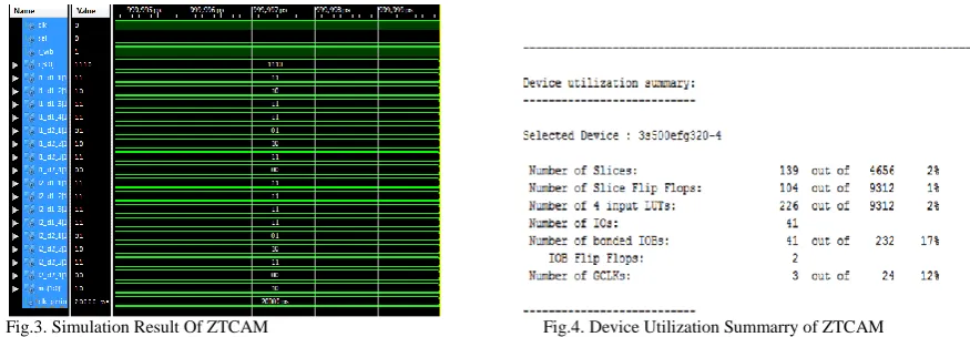
The proposed design is developed using VHDL and synthesized using XILINX 13.2 and is simulated in Isim Spartan-3E FPGA series. The simulation result of the ZTCAM is shown in Fig.3. Here c[3:0], sel ,r_wb are the three inputs of the ZTCAM. When sel = 0, only the operations takes place. When the data is input, the potential match address is produced at the output. When r_wb=1,read operation takes place. When r_wb=0,write operation takes place. When sel=1,it goes to high impedance state. The data is input and it is divided in to N sub words. It is then given as address to the validation memory .The same sub word is given to the OATAM. Here, the data given is the 1110 and the match address provided is 10.
Fig.3. Simulation Result Of ZTCAM Fig.4. Device Utilization Summarry of ZTCAM
The device utilization summary of ZTCAM is given in Fig.4. The number of slices used is 139 out of 4656 and the number of slice flip flops are 104 out of 9312. The number of 4 input LUTs are 226 out of 9312,IOs are 41,bonded IOBs are 41 out of 232,,IOB flip flops are 2 and number of GCLKs are 3 out of 24.
The simulation results of the area efficient ZTCAM are shown below. Here c[3:0],sel, r_wb are the three inputs of the modified area efficient ZTCAM. When sel = 0,only the operations takes place. When the data is input, the potential match address is produced at the output. When r_wb=1,read operation takes place. When r_wb=0,write operation takes place. When sel=1,it goes to high impedance state. The data is input and it is divided in to N sub words. It is then given as address to the validation memory .The same sub word I given to the OAT.OATAM is removed and the functionality is obtained using OAT. The modification is done in data mapping operations. Here, the data given is the 1101 and the match address provided is 11.
Address VM11
VM12 OAT11
OAT 21
0 1 0 1
0 1 2 3 1
0
1
1
0
0
0
1
1 0 0 0
0 1 0 1
0 0 0 0
ISSN(Online): 2320-9801
ISSN (Print): 2320-9798
I
nternational
J
ournal of
I
nnovative
R
esearch in
C
omputer
and
C
ommunication
E
ngineering
(An ISO 3297: 2007 Certified Organization)
Vol. 3, Issue 9, September 2015
Fig.5. Simulation Result Of Area Efficient ZTCAM Fig.6. Device Utilization Summarry of Area Efficient ZTCAM
The device utilization summary of area efficient ZTCAM is given below. The number of slices used is 105 out of 4656 and the number of slice flip flops are 76 out of 9312.The number of 4 input LUTs are 174 out of 9312, IOs are 41, bonded IOBs are 41 out of 232,IOB flip flops are 2 and number of GCLKs are 3 out of 24.When the device utilization summary of ZTCAM and modified area efficient ZTCAM are compared, it can be seen that the number of slices, slice flip flops,4 input LUTs are reduced. This indicates that the area has been reduced which increases the performance and reduces the power as well as cost.
Fig.7. Simulation Result Of Area Efficient ZTCAM with clock Gating Table 4. Comparison Of Area And Delay
.
The simulation results of the area efficient ZTCAM with clock gating is shown in Fig.7. The input is accessed only when the clock enable signal is on. Thus it helps in an efficient power management scheme. Table 4shows the comparison between ZTCAM and modified ZTCAM. From this it is clear that the modified architecture makes it more area efficient without affecting the performance.
Parameter Area(slices out of 4656)
Delay
ZTCAM 139 4.03
Area Efficient ZTCAM
ISSN(Online): 2320-9801
ISSN (Print): 2320-9798
I
nternational
J
ournal of
I
nnovative
R
esearch in
C
omputer
and
C
ommunication
E
ngineering
(An ISO 3297: 2007 Certified Organization)
Vol. 3, Issue 9, September 2015
V. CONCLUSION
The objective to design and implement a low cost and area efficient ZTCAM is achieved. The clock gating was also applied to the area efficient ZTCAM and thereby achieved efficient power management a. The modification of the ZTCAM architecture by removing the OATAM and modifying the data mapping operation is performed and this results in a low cost and area efficient architecture ZTCAM.
REFERENCES
1. Z-TCAM: An SRAM-based Architecture for TCAM Zahid Ullah, Manish K. Jaiswal, and Ray C. C. Cheung
2. N. Mohan, W. Fung, D. Wright, and M. Sachdev, “Design techniques and test methodology for low-power TCAMs,” IEEE Trans.Very Large Scale Integr. (VLSI) Syst., vol. 14, no. 6, pp. 573–586,Jun. 2006.
3. P. Mahoney, Y. Savaria, G. Bois, and P. Plante, “Parallel hashingmemories: An alternative to content addressable memories,” in Proc.3rd Int. IEEE-NEWCAS Conf., Jun. 2005, pp. 223–226.
4. W. Jiang and V. Prasanna, “Parallel IP lookup using multiple SRAMbased pipelines,” in Proc. IEEE Int. Symp. Parallel Distrib. Process.,Apr. 2008, pp. 1–14.
5. S. Cho, J. Martin, R. Xu, M. Hammoud, and R. Melhem, “CA-RAM:A high-performance memory substrate for search-intensive applications,”in Proc. IEEE Int. Symp. Perform. Anal. Syst. Softw., Apr. 2007,pp. 230–241. S. V.
6. Kartalopoulos, “RAM-based associative content-addressable memory device, method of operation thereof and ATM communication switching system employing the same,” U.S. Patent 6 097 724, Aug. 1, 2000. M. Somasundaram, “Memory and power efficient mechanism for fast table lookup,” U.S. Patent 20 060 253 648, Nov. 2, 2006.
7. M. Somasundaram, “Circuits to generate a sequential index for an input number in a pre-defined list of numbers,” U.S. Patent 7 155 563, Dec. 26, 2006.
8. [9] D. E. Taylor, “Survey and taxonomy of packet classification techniques,” ACM Comput. Surveys, New York, NY, USA:Tech. Rep. WUCSE-2004-24, 2004.
9. P. Mahoney, Y. Savaria, G. Bois, and P. Plante, “Transactions on high performance embedded architectures and compilers II,” in Performance Characterization for the Implementation of Content Addressable Memories Based on Parallel Hashing Memories, P. Stenström, Ed. Berlin,Germany: Springer-Verlag, 2009, pp. 307–325.
10. W. Jiang and V. Prasanna, “Scalable packet classification on FPGA,”IEEE Trans. Very Large Scale Integr. (VLSI) Syst., vol. 20, no. 9,pp. 1668–1680, Sep. 2012.
11. M. Becchi and P. Crowley, “Efficient regular expression evaluation: Theoryto practice,” in Proc. 4th ACM/IEEE Symp. Archit. Netw. Commun.Syst., Nov. 2008, pp. 50–59.
12. Xilinx, San Jose, CA, USA. Xilinx FPGAs [Online]. Available:http://www.xilinx.com
13. W. Jiang and V. K. Prasanna, “Large-scale wire-speed packet classification on FPGAs,” in Proc. ACM/SIGDA Int. Symp . Field Program. GateArrays, 2009, pp. 219–228.
14. K. Pagiamtzis and A. Sheikholeslami, “Content-addressable memory(CAM) circuits and architectures: A tutorial and survey,” IEEE J. Solid-State Circuits, vol. 41, no. 3, pp. 712–727, Mar. 2006.
15. Xilinx, San Jose, CA, USA. Xilinx Xpower Analyzer [Online]. Available: 16. http://www.xilinx.com
17. S.-J. Ruan, C.-Y. Wu, and J.-Y. Hsieh, “Low power design ofprecomputation-based content-addressable memory,” IEEE Trans. VeryLarge Scale Integr. (VLSI) Syst., vol. 16, no. 3, pp. 331–335, Mar. 2008.H. Noda et al., “A cost-efficient high-performance dynamic TCAM with pipelined hierarchical searching and shift redundancy architecture,” IEEEJ. Solid-State Circuits, vol. 40, no. 1, pp. 245–253, Jan. 2005. 18. W. Jiang, V.K. Prasanna, N. Yamagaki, Decision forest: a scalable architecture for flexible flow matching on FPGA. In Proceedings of the
2010 International Conference on Field Programmable Logic and Applications, FPL ’10, pp. 394–399 (2010).
19. Z. Ullah, K. Ilgon, S. Baeg, Hybrid partitioned SRAM-based ternary content addressable memory. Circuits Syst. I 59(12), 2969–2979 (2012)
BIOGRAPHY