A Proposed FPGA Based Architecture to
Implement EOS Component of an Automatic
Cartoon Movie Builder (ACMB) System
Santanu Halder1,Ranjit Kumar Mandal2, Debotosh Bhattacharjee3, Mita Nasipuri4
Associate Professor, Department of Computer Application, Kalyani Govt. Engineering College, Nadia, WB, India1
Assistant Professor, Department of Computer Science and Engineering, Government College of Engineering and
Ceramic Technology, Kolkata, India2
Associate Professor, Department of Computer Science and Engineering, Jadavpur University, Kolkata, India3
Professor, Department of Computer Science and Engineering, Jadavpur University, Kolkata, India4
ABSTRACT: This paper aims to design a FPGA based system to implement a part of our main research work called ACMB (Automatic Cartoon Movie Builder) system which generates a cartoon movie based on a given story collected from the user. The system has two types of databases: (a) Movie Database (DB-M) consisting of cartoon movies (animations) collected from different sources (b) Frame Database (DB-FR) consisting of shots (or sequence of frames depicting a continuous action) extracted from the movies of DB-M along with their textual characterization. The ACMB system has the following features: (i) Extraction of shots (or sequence of frames) from the movies stored in DB-M (ii) Characterization of extracted shots and storing them in the database DB-FR (iii) Conversion of user given story into the machine understandable form (iv) Searching of shots from database DB-FR according to the characterized form of input story (v) Generation of cartoon movie with the retrieved shots and storing the generated movie in database DB-M if accepted by the user (vi) Modification of selected frames of the generated movie if required by the user. Now the types of modification in the present system could be of four types: (a) Color adjustment of the selected frames (b) Brightness adjustment of the selected frames (c) Speed adjustment of the selective frames in the movie and (d) Introducing End Of Scene (EOS) sequence after a selected frame in the generated movie. In this paper, we focus on the FPGA implementation EOS type modification of the generated movie. The proposed method has been tested on the frames of 1000 shots which are extracted from 10 movies stored in DB-M.
KEYWORDS: Frames, Shots, EOS, FPGA.
I. INTRODUCTION
movie if required by the user. The type of modifications can be of four types: (a) Color adjustment of the selected frames (b) Brightness adjustment of the selected frames (c) Speed adjustment of the selective frames in the movie and (d) Introducing End Of Scene (EOS) sequence after a selected frame in the generated movie. The main focus of this paper is to design FPGA based architecture of the last type of modification which may be useful for designing a real time application of the ACMB system. FPGA is becoming the most dominant form of programmable logic [3-5] over the past few years and it has advantages of low investment cost and desktop testing with moderate processing speed and thereby offering itself as suitable one for real time application and a lot of research work is being carried out on the FPGA implementation in various field [6-8]. This work is an initial attempt towards the designing of a real time application for all the features of the ACMB system
This paper is organized as follows: The section II presents the brief description of the ACMB system. Section III describes the proposed methodology. Section IV shows the top level design. Section V depicts the system architecture. Section VI shows the experimental results and finally section VII concludes and remarks about some of the aspects analyzed in this paper.
II. THE ACMBSYSTEM
FEM: Frame Extractor Module FCM: Frame Characterization Module TAM: Text Analyzer Module FRM: Frame Retrieval Module MGM: Movie Generator Module LSM: Line Specifier Module TMSM: Type of Modification Specifier Module IMGM: Interactive Movie Generator Module
Fig.1: Block diagram of the ACMB system
III.PROPOSED METHODOLOGY
The present system takes a frame as specified by the user and then applies the image morphing technique to generate the required number of frames in between the specified frame and the finally generated black frame (a frame which contains all zero values). Let the frame be denoted as I(i,j,k) and the size of the frame is
p
q
. In the present system, an user may specify the number of frames (N) to be specified directly or by stating the time duration (t). Here, the frame rate has been assumed as 15 frames/sec. Hence, for time t, the value of N is 15t. The logic to generate the intermediate frames is to subtract the value of intensities of the specified frame by a constant term Di for N time’srecursively. The value of Di is different for Red, Green and Blue channels. Let the values of Di for three channels are
DR, DG and DB respectively and the intensity values of the three channels for the current pixel are R, G and B
respectively. The proposed methodology uses Eq. 1 to Eq. 4 to find the value of DR, DG and DB.
N
D
1
(1)
D
R
D
R
Old
(2)
D
G
D
G
Old
(3)
D
B
D
B
Old
(4)
Now the system find the new pixel intensities of Red, Green and Blue channel using Eq. 5 to Eq. 7.
FEM TAM FCM FRM MGM LSM Accepted? TMSM IMGM Frame Database (DB-FR) Yes No No
Yes Movie Database (DB-M) Movie Generated Movie Story Rewrite Story?
Fig.2: An example showing the step of the proposed methodology
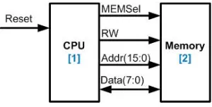
IV.TOP LEVEL DESIGN
The top level design of the proposed architecture is shown in Fig. 3. It contains two modules: (1) CPU and (2) Memory. The control signals are Reset, MEMSel and RW. When the value of Reset is ‘1’, then the CPU starts its execution. The signal MEMSel is used to select the memory to read or write. When the control signal RW is set, then it indicates a memory read operation and when it is reset, then it indicates a memory write operation. A 16-bit address bus and a 8-bit data bus is used in the current system
.
Fig.3: Top level design of the proposed system
V. SYSTEM ARCHITECTURE
Fig.4: Block diagram of CPU unit
A. MEMORY UNIT
The memory unit is a part of the system that holds data. In the present system, a
2
13
8
bit memory unit has been designed using VHDL to store the input data and output data assuming that the size of each frame could be of maximum90
75
pixel. This unit is controlled by a global clock. it has four ports out of which three (ADDR, R/W, MEMSEL) are input ports and one (DATA) is input/output port. When the MEMSEL and R/W signal is 1, the memory unit reads the data from the location specified by the 16-bit address bus (ADDR) and places the data in the 8-bit data bus (DATA). Again when the value of the MEMSEL is 1 and R/W is 0, the memory unit writes the data (which resides in data bus) at the location specified by the address bus. If the value of the MEMSEL is 0, the memory unit is disabled.B. PROGRAM COUNTER AND ADDER/SUBTRACTOR UNIT
The Program Counter (PC) is basically a 16-bit register which holds the memory address to be currently accessed. When RESET signal is ‘1’, the control unit sets the value of PCSel and when the value of PCSel is ‘1’ the program counter resets it’s content to ‘00000000’. In other cases, the program counter propagates the input address to the Adder unit. The Adder/Subtractor unit increments it’s input by 1 when the value of IncSel is ‘01’ or ‘11’, keeps the value unchanged for ‘00’ value of IncSel and decrements its input by 1 when the value of IncSel is ‘10’. After processing, the Adder/Subtractor unit stores the result in program counter as the next memory address. In the present work, the current system overwrites the existing intensity value by the calculated value which is generated through the PU module. That’s why, the decrement of program counter value is necessary to go back to the memory position where the old value was stored.
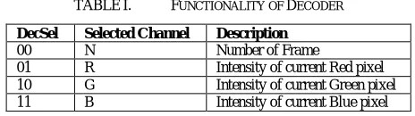
C. DECODER
This module is used to route the data in the different channel in separate clock cycles. This module takes two inputs: (i) Din is 8 bit and (ii) DecSel in 2 bits. There are four output channels of this module as shown in Fig. 4. Depending on the
value of DecSel, this module propagates the value of Din in a particular channel as shown in Table I.
of RegSel is ‘01’, then the content of Reg1 is placed on the data bus and for the RegSel value of ‘10’, the content of the Reg2 is placed on the data bus.
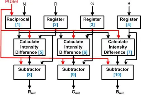
E. PROCESSING UNIT
The processing unit (PU) of the proposed architecture is responsible to compute the new pixel intensity values to implement the End of Scene (EOS) type modification over the selected frames in the generated movie. The block diagram of the PU unit is shown in Fig. 5.
Fig.5: Block diagram of Processing Unit
There are ten modules in the PU unit out of which three modules are Register modules which are used to hold the values of red, green and blue channel of the pixel under consideration for the further processing. Rests of the modules are activated by a select line called PUSel as shown in Fig 5. When all input data of this unit are available, then the control unit sets the value of PUSel and PU starts its execution. Hence the modules of this unit are active for the ‘1’ value of PUSel.
The first module takes the number of frame (N) to be generated as input and finds the reciprocal value of it according to Eq. 1. This module is implemented using a Look Up table (LUT) which stores the reciprocal value of all binary numbers in 8-bit.
The module numbers 5, 6 and 7 are similar in nature which calculates the value of DR, DG and DB according to Eq. 2, Eq. 3 and Eq. 4 respectively.
Finally, module 8, 9 and 10 take the value of R, G and B of the current pixel position and finds the new pixel intensity values using Eq. 5, Eq. 6 and Eq. 7 respectively.
F. CONTROL UNIT
Fig.6: State diagram of the Control Unit
When the RESET signal is ‘1’, the system enters into state 0. In state 0, CU sets the value of PCSel to reset the content of program counter to “00000000”, reset the value of IncSel to indicate no increment of program counter and resets the value of PUSel to indicate no operation in processing unit. In the next clock cycle, if the value of RESET is ‘0’, then the system enters into state 1. In state 1, state 2, state 3 and state 4, the control unit reads the value of N (number of frame), R (Current intensity of Red), G (Current intensity of Green) and B (Current intensity of Blue) respectively. From State 5 to State 7, the processing unit finds the value of new R, G and B values and stores the calculated values in the register array. In state 8, the control unit stores the new R value in the position of its old value in the memory. Similarly it stores the new G and B values in state 9 and 10 respectively. As the value of N needs to be fetched only once at the start of the processing, so after state 10, the control unit goes to state 2 from where it starts to read the new pixel intensity values in RGB. These steps are continued until end of the file and after each iteration the system stores the new set of values in memory and again starts the process from the beginning. After each iteration, the system decrement the value of N and stores it into the first position of the memory location which is subsequently used by the system for the next course of action.
VI.EXPERIMENTAL RESULTS
Fig.7: Device utilization summery
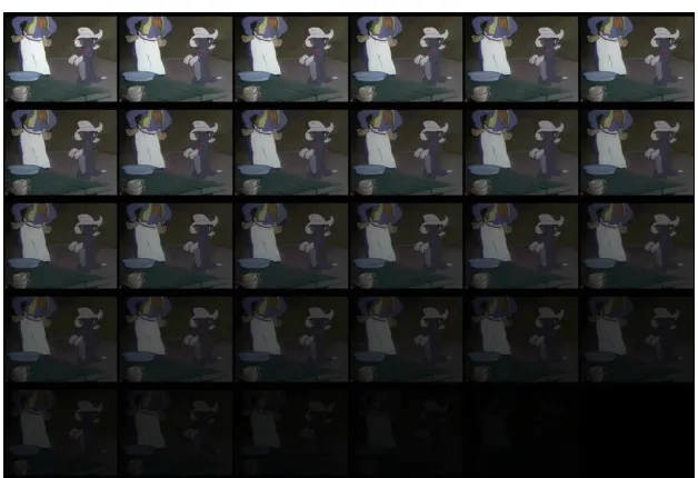
Few experimental results are shown in Fig. 8 to Fig. 11.
Fig.8: Problem frame 1
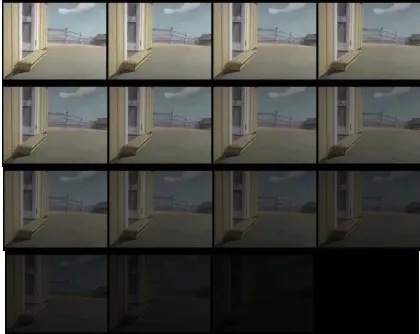
Fig. 9: Sequence of frames generated for the frame of Fig. 8 for N=30
Fig. 11: Sequence of frames generated for the frame of Fig. 10 for N=16
VII. CONCLUSION
In this paper, we propose a FPGA based implementation of the EOS component which is a part of our main research effort called Automatic Cartoon Movie Builder (ACMB) system. FPGA implementation of this type of work is new in the literature. Our approach is tested on a frame database including over 1000 shots collected from 10 cartoon movies.
REFERENCES
[1] PATEL N. V., SETHI I. K.: Video shot detection and characterization for video databases. Pattern Recognition 30 (1997), 538–592
[2] S Halder, R. K. Mandal, D. Bhattacharjee, M. Nasipuri, “Design of an Automatic Cartoon Movie Builder (ACMB) System for Generation of a Cartoon Movie from a given story”,IEEE International Conference on Computational Intelligence and Communication Network, 14-16th November 2014, Kolkata.
[3] Jenkins, Jesse H. (1994), Designing with FPGA and CPLDs, Prentice-Hall Publication.
[4] Weste N.H.E., Eshraghian K. (2000), Principles of CMOS VLSI Design: A Systems Perspective, Pearson Education Asia.
[5] Wakerly J. F. (2002), Digital Design: Principles and Practices, Pearson Education,Asia.
[6] D. Bhattacherjee, S. Halder, M. Nasipuri, D.K. Basu, M. K. Kundu, “FPGA Based Assembling of Facial Components for Human Face Construction”, International Journal of Recent Trends in Engineering, ACEEE, Vol. 1, No. 1, May 2009, pp. 541-545.
[7] S. Halder, D. Bhattacherjee, M. Nasipuri, D.K. Basu,, “A Fast FPGA Based Architecture for Sobel Edge Detection,” 16th International Symposium on VLSI Design and Test, VDAT 2012, 01-04th July 2012.