Available online: https://edupediapublications.org/journals/index.php/IJR/ P a g e | 484
Design and Simulation of Ping-Pong Auto Zero Opamp
Abhimanu Surendra K Singh
& Poonam Pathak
#Electronics & Communication, R.G.P.V Bhopal L.K.C.T. Indore M.P. India
Abstract—
A wide variety of electronic applications deal with small signal inputs. These systems need to have very low offset as well as very low offset drift over time and temperature. High precision is required in these fields. Such fields like instrumentation, automotive and industrial applications require precision amplifiers within reasonable cost and simplicity. The amplifiers by far having the lowest possible offset and offset drift is the auto zero amplifier. In this thesis we describe a precision opamp using ping pong auto zero architecture , which is capable of very low offset and offset drift over temperature along with producing continuous output. The architecture has been designed to operate in extreme environments under a wide temperature. The simulated results show that the amplifier is fully functional and capable of less than 15uV of input referred offset voltage. The design has been carried out in cadence 0.18um technology. It consumes 4.2mW of power and has a offset drift over temperature 3.5uV/0C.Keywords—EDA Tanner, T-Spice, CMOS, PMOSFET, NMOSFET.
I.
Introduction
The name ping pong implies two and forth action. It
consists of 2 identical amplifiers, switch, sample and hold
circuit and switch driver. the requirement of this design
arises from the matter that motorcar zero electronic
equipment cannot alone turn out continuous output. As we
have a tendency to recall from chapter three, motorcar
zero amplifiers operate in 2 phases. Throughout one
section, amplification and through another sampling is
finished. Hence, it cannot turn out continuous output. The
ping malodour on the opposite hand employs 2 motorcar
zero identical amplifiers such either one amongst them
invariably processes the signal, therefore manufacturing
an eternal output. Also,at a similar time either one
amongst them will the offset cancellation creating it
conjointly continuous. Finally, we have a tendency to get
an offset free continuous output.
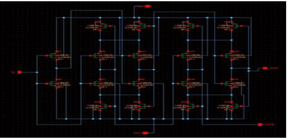
The ping pong auto zero block diagram is shown below:
Fig 1: Ping-Pong auto zero opamp block diagram.
The opamp as usual consists of two inputs Vin+ and Vin along with VDD and VSS dual power in fig.
Available online: https://edupediapublications.org/journals/index.php/IJR/ P a g e | 485
Fig 2: Inner Blocks of Ping-Pong auto zero opamp.
II. Components of Ping-Pong Architecture
Opamp employing Auto zero
An auxiliary input try is more to the classical 2 stage opamp
so as to form it motorcar zero electronic equipment. 2 such
identical amplifiers ar required for the ping malodour design.
The gain of the fundamental opamp is split into two equal
elements i.e. Ab becomes Av/2 for each input in addition as
auxiliary input try. Hence, now the gain of the motorcar zero
electronic equipment becomes Ab/2 as compared to achieve
of basic Opamp that is Av. conjointly the gains of main and
auxiliary input pairs becomes equal. The schematic is same
as shown in Fig.
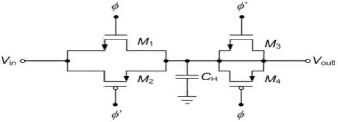
Sample and Hold Circuit
The sample and hold circuit is that the most vital circuit as
per the accuracy of the planning. The work of the sample
and hold circuit is to sample the input offset voltage
throughout the sampling section and so to carry it
throughout the amplification section. So, the offset gets off
throughout the amplification section. Hence, we get
associate offset free amplification of the signal. The sample
and hold circuit is designed by employing a nmos
asynchronous with electrical device. This is often the only
sample and hold circuit. But, the matter with this circuit is
“charge injection effect” that makes it not appropriate for
this style. This style wants an extremely correct S & amp; H
circuit. Charge injection Effect: throughout the on or
conductivity section, a channel develops between the
Available online: https://edupediapublications.org/journals/index.php/IJR/ P a g e | 486
(acts as capacitor) stores some charge throughout the on
section. once the NMOS becomes off, the keep charge gets
shared between the input supply and therefore the holding
electrical device. once the charge gets injected into the
electrical device, the output becomes inaccurate.
Fig 3: Simple sampling circuit.
The charge stored is given by,
Qst = WLCOX(VDD – VIN –
Vth)
The residual voltage on the capacitor during off state is
given by,
ΔV = (WLCOX(VDD – VIN – Vth))/CH
There is conjointly another undesirable impact related to
the higher than sampling circuit. It’s known as clock feed
through impact.
Clock feed through Effect:
Throughout the high to low transition of the clock signal
the gate-drain and gate-source overlap capacitance in
conjunction with holding capacitance type a path between
clock input and ground. Hence, a resistance circuit is
made between clock and output. It creates an error within
the output worth.
The residual or erroneous voltage across CH is given by,
ΔV = Vclk Cgd/(Cgd + CH)
Fig 4: Clock feed through effect.
However, by increasing worth of CH and decreasing
worth of W/L quantitative relation each the consequences
can be stipendiary to some extent. Complementary switch
and dummy switch area unit the 2 approaches adopted
during this project for reducing the higher than 2 effects.
Complementary switch is structure holding a NMOS
Available online: https://edupediapublications.org/journals/index.php/IJR/ P a g e | 487
Fig 5: Complementary Switch.
Here, because the charge carried by NMOS is opposite in
polarity to charge carried by PMOS, the charge injected
by the NMOS are off throughout the off part by PMOS.
But, each the fees magnitude should be same.
Unfortunately, the gate drain overlap capacitance isn't
same in NMOS and PMOS. Therefore, this mechanism
cannot cancel the charge injection utterly. Reduction of
on resistance is one in every of it’s extra advantage. On
the opposite hand, dummy switches may also use to cut
back the errors.
Fig 6: Dummy switch.
As shown within the higher than figure, throughout the off
part (M1 is off and money supply is on) the charge injected
from M1 finds means through money supply , as money
supply is on and there's a formation of channel between
gate to supply of money supply. This channel absorbs the
charge injected from M1.Similarly,when M1 is on and
money supply is off, the charge injected from money
supply finds means through M1 to the low electrical
resistance signaling. Hence, the output remains error be
no delay between the Ǿ and Ǿ’.
To get an even better solution, both
Fig 7: Complementary switches with dummy switches
In this, CH = 5u
(W/L)1 = 10
(W/L)2 = 4
Available online: https://edupediapublications.org/journals/index.php/IJR/ P a g e | 488
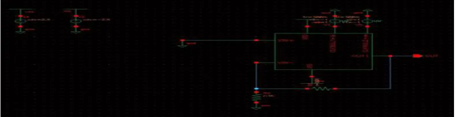
Fig 8: Sample and hold circuit with switch driver
Switch and Switch Driver
Simply mistreatment AN electrical converter might harm
the terribly purpose of the on top of sample and hold circuit.
the requirement of concurrent on and off of the M1, M2 and
M3,M4 transistors severally provides rise to clock driver. It
generates 2 overlapping signals and provides low clock
skew between the 2 signals.
Fig 9: Switch Driver Schematic.
In this project, cmos transmission gate is used as the switch with (W/L) of nmos set as 10 and (W/L) of pmos set as 4.
Available online: https://edupediapublications.org/journals/index.php/IJR/ P a g e | 489
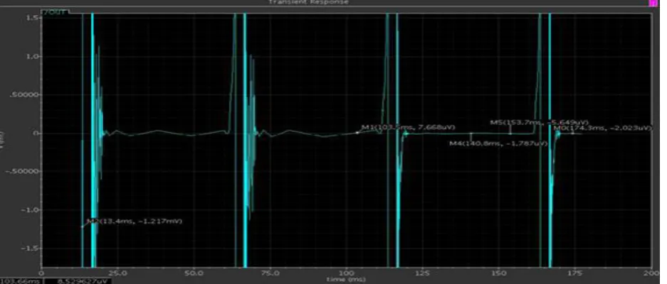
Fig 9: Output offset voltage of opamp.
Fig 10: Output offset voltage of Ping-Pong amplifier.
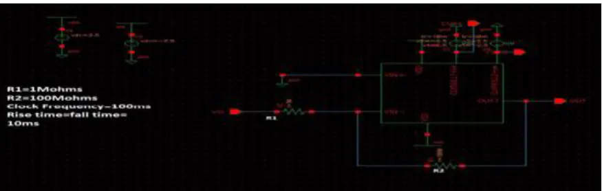
Fig 11: Measurement setup of
Available online: https://edupediapublications.org/journals/index.php/IJR/ P a g e | 490
Fig 12(i): Offset cancellation of
Fig 13(ii): Offset cancellation measurement set up.
An intentional ten mV of offset is another to at least one of
the inputs (non-inverting) of each the motor vehicle zero
amplifiers within the ping mephitis design. The simulation
lead to Fig (i) and (iii) shows the offset cancellation is
finished with success to a median 4uV throughout any of the
clock part. Fig (ii): Offset cancellation of ping mephitis
Available online: https://edupediapublications.org/journals/index.php/IJR/ P a g e | 491
Fig 14(ii): Offset cancellation of ping pong amplifier.
a.
Other parameters of Ping-Pong amplifier
Available online: https://edupediapublications.org/journals/index.php/IJR/ P a g e | 492
Fig 16: CMRR of ping pong amplifier
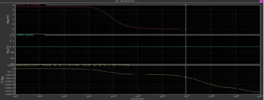
Fig 17: Phase margin of ping pong amplifier.
PM of ping pong amplifier from above diagrams calculated as 470.
Fig 18: Offset vs. temperature drift of ping pong amplifier.
Available online: https://edupediapublications.org/journals/index.php/IJR/ P a g e | 493
Fig 19: power consumption of ping pong amplifier.
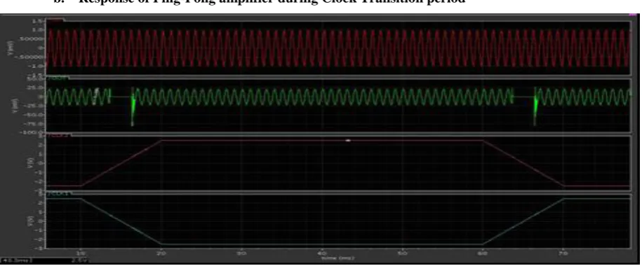
b. Response of Ping-Pong amplifier during Clock Transition period
Fig 20: Discontinuity of output during clock transition.
The circuit for the above simulation is in non-inverting configuration with RF = 20ML and RIN =1ML.
IV.
CONCLUSION
The design was tested for terribly low offset and
automatic offset cancellation. it had been with success
enforced. But ICMR, output ranges were severely
affected in conjunction with separation of output. Still
the gain and also the slew rate got to be improved. More
correct switch and S & amp; H circuits with doubled
cascade opamp design can provide higher results.
REFERENCES
[1] Christian C. Enz and Gabor C. Temes, “Circuit
Techniques for Reducing the Effects of Op-Amp
Imperfections: Autozeroing, Correlated Double
Sampling, and Chopper Stabilization,” Proceeding of the
IEEE, vol. 84, pp.1584-1614, November 1996.
[2] Ion E. Opris and Gregory T. A. Kovacs, “A
Rail-to-Rail Ping-Pong Op-Amp,” IEEE Journal of Solid-State
Available online: https://edupediapublications.org/journals/index.php/IJR/ P a g e | 494
[3] Stephen C. Terry, Benjamin. J. Blalock, Jeremy R.
Jackson, Suheng, Chen, et al, “Development of Robust
Analog Electronics at the University of Tennessee for
NASA/JPL Extreme Environment Applications,”
Proceedings of the 15th Biennial
University/Government/Industry Microelectronics
Symposium, pp.124-127, June 2003.
[4] Paul. R Gray, Paul J. Hurst, Stephen H. Lewis and
Robert. G. Meyer, Analysis and Design of Analog
Integrated Circuits, Fourth Edition, Wiley, 2001
[5] Ron Hogervorst, John P. Tero, Ruud G. H. Eschauzier,
and Johan H. Huijsing, “A Compact Power-Efficient 3 V
CMOS Rail-to-Rail Input/Output Operational Amplifier
for VLSI Cell Libraries,” IEEE Journal of Solid-State
Circuits, vol. 29, no. 12, pp.1505-1513, December 1994.
[6] S. Chen, S. C. Terry, C. Ulaganathan, B. J. Blalock,
M. M. Mojarradi, “A SiGe Current Reference for Low
Temperature Analog/Mixed-Signal Applications,”
Seventh International Workshop on Low Temperature
Electronics, June 2006.
[7] D. M. Binkley, B. J. Blalock, and J. M. Rochelle,
“Optimizing Drain Current, Inversion Coefficient, and Channel Length in Analog CMOS Design,” Journal of
Analog Integrated Circuits and Signal Processing, vol. 47,
no. 2, May 2006, pp. 137-163.
[8] R. L. Greenwell, S. C. Terry, B. J. Blalock, M. M.
Mojarradi, and E. Kolawa, “5-V Compatible
Radiation-Hardened SOI Rail-to-Rail Input/Output Operational
Amplifier for Extreme Environments,” Government
Microcircuit Application and Critical Technology
Conference, March 2007.
[9] B. Minch, “A Low-Voltage MOS Cascode Bias Circuit for All Current Levels,” Proceedings of the
International Symposium on Circuits and Systems, vol.
III, May 2002
[10] A. Abo, “Design for Reliability of Low-voltage, Switched-capacitor Circuits,” Ph.D. dissertation,
University of California, Berkeley, May 1999.
[11] G. Wegmann, E. A. Vittoz, and F. Rahali, “Charge Injection in Analog MOS Switches,” IEEE Journal of
Solid-State Circuits, vol. SC-22, no. 6, pp.1091-1097,
December 1987.
[12] Behzad Razavi, Design of Analog CMOS Integrated
Circuits, McGraw, 2000
[13] Tony Antonacci and Robert Greenwell, “Opamp Characterization User Reference Manual,” July 2006
Edition.
[14] Stephen C. Terry, “Low-Voltage Analog Circuit
Design Using the Adaptively Biased Body- Driven
Circuit Technique,” Ph.D. dissertation, University of
Tennessee, Knoxville, August, 2005.
[15] P.E. Allen and D.R. Holberg, CMOS Analog Circuit