VLSI Design and Implementation of Schmitt
Trigger based VCO for PLL Architecture
Purnima1, Radha B. L2, Kumaraswamy K. V3
PG Student [VLSI], Dept. of ECE, Bangalore Institute of Technology (BIT), Bengaluru, India1
Associate Professor, Dept. of ECE, Bangalore Institute of Technology (BIT), Bengaluru, India2
Technical Manager, Trident Techlabs Private limited, Bengaluru, India3
ABSTRACT: this paper proposes the transient and phase noise analysis of Schmitt trigger circuit based CSVCO which will give clean square pulses from noisy input signals with less phase noise and also applicable for low power. This Schmitt based CSVCO is used in PLL architecture which further can be applicable for frequency synthesis, data recovery, tracking input signals such as in tracking generators(ex: car’s cruise control),clock generation etc. After simulation i.e., after performing analysis of phase noise it provides phase noise of -106dbc/Hz at the offset frequency of 1MHz. This transient and phase noise simulation is performed in Mentor Graphics tool i.e., Pyxis (eldo) in 130nm technology.
KEYWORDS: PLL(Phase Locked Loop), PD(Phase detector), LPF(Low pass filter), CSVCO(Current starved VCO), VCO(Voltage controlled oscillator), CP(Charge Pump).
I.INTRODUCTION
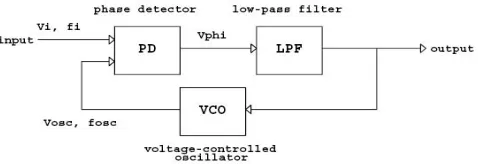
In this paper the PLL is a phase locked loop which is a negative feedback system where we are locking the two phases i.e., the input phase is compared with the output phase which is the result of Schmitt trigger based CSVCO. PLL is generally a synchronizing circuit which synchronizes the output signal which is the result of Schmitt based CSVCO with the reference input signal. The objective of this paper is to generate the clean square pulses even though there is a noisy input signals from the VDD variation. Where this is very important in order to get locked condition properly or fine tune of PLL. In PLL VCO is heart of the architecture so we have to tune it properly to get locked. This Schmitt based CSVCO can be used in wireless communication (satellite communication) applications. The Block diagram for PLL is shown in figure below which consists of:
1. PD(Phase Detector) 2. CP(Charge Pump) 3. LPF(Low Pass Filter)
4. Schmitt based current starved VCO(CSVCO)
Figure 1 Block diagram of PLL
The paper is organized as related work in section ІІ, proposed methodology in section ІІІ, equations in section
ІV,measurement, simulation results and waveformsin section V and conclusion in section VІ.
ІІ. RELATED WORK
In previous PLL design they were using ring oscillator based VCO where, in order provide high tuning range or frequency range they were increasing VDD that means tuning range is dependent on VDD. If we increase VDD by ±10 we used to get frequency range from 1-3GHz but VCO will become unstable. So to make independent of VDD we are increasing tuning voltage to get high frequency range.
IIІ.PROPOSED METHODOLOGY
Phase Detector with Charge Pump:Usually PD will compare the phases of two input signals and produces output voltage. If the phases of two signals are different then it produces up and down pulses. The error voltage is produced by integration and subtraction of these up and down pulses in order to tune or control the VCO. This error voltage is fed to the charge pump in order to pump in and pump out the charge from LPF in order to increase or decrease the control voltage required for VCO.
Charge Pump is basically used to convert the digital pulses produced by up and down signals into continuous signals as analog one.
LPF: The output of PD usually consists of high frequency as well as dc components where first component is undesired so LPF is used to attenuate the high frequency components coming from the PD output and hence passes the dc to the Schmitt based CSVCO to tune it.
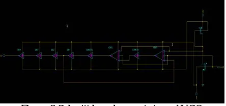
Schmitt based CSVCO: we are using Schmitt based CSVCO in order to produce clean square pulses even in the variation of VDD or input voltage coming from LPF which produces noisy signals.Instead of varying the supply voltage VDD in order to tune the VCO to get a frequency range from few Hzs to thousands of Hzs we are varying the control voltage which will acts as input voltage coming from LPF as shown in below figure 2. The operation of below VCO is similar to that of normal ring oscillator.
Figure 2 Schmitt based current starved VCO
As normal topology it is followed by inverters at the end. In this circuit we are using Schmitt trigger circuit in betweencurrent starved inverters to get clean square pulses. As we know that inverters are starved or hungry for current so we are using current starved inverters instead of normal inverters which will limit the current in order to charge or discharge the internal node capacitance of the MOS devices. Further in order to maintain the constant current inside each inverter we are using current mirror circuit at the input stage as shown in above figure 2.
The above VCO starts to oscillate when vin≥ vthn it will produces maximum frequency when vin=VDD and minimum frequency when vin=vthn and normally stops oscillating when input voltage is less than threshold i.e., because NMOS will enter into cut off region (vin˂vthn).
Where
And N is number of stages
The internal total capacitance at the input and output node is given as
The MOSFETs M1 and M2 at the input stage acts as current sources to maintain drain current inside the inverters which is set by Vcont.
The frequency ranges for different values of control voltage set by the control mechanism is given in below table (1). Table 1 frequency ranges
ІV. EQUATIONS
The closed loop transfer function of PLL that is given below in the form of mathematical description of both VCO and PD
The above equation is obtained from evaluation of below figure3. Where,
Positive sign = for positive feedback Negative sign= for negative feedback
=the closed loop transfer function G(s) = forward transfer function H(s) = feedback transfer function G(s)H(s) = open loop transfer function
V. MEASUREMENT, SIMULATION RESULTS AND WAVEFORMS
The above designed PLL is used in many applications such as wireless application. It is designed using 130nm technology Mentor Graphics tool.
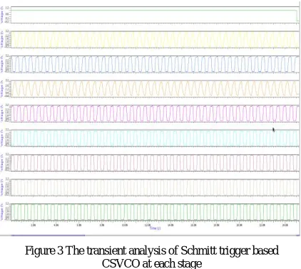
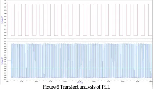
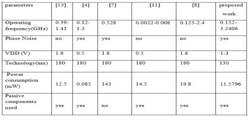
The above Schmitt based CSVCO will work for supply voltage of 1V-3V.The PLL is designed using 130nm CMOS technology with 1.9v supply voltage. The transient analysis of Schmitt trigger based CSVCO at each stage is given in figure (4). The power consumed by Schmitt based CSVCO is 240.411uW for 1v supply and for 3V it consumes 11.579mW.The transient analysis of complete integrated PLL is shown in figure (7) where red colour waveform is reference input signal and green one is control input voltage to CSVCO and blue is resultant signal from Schmitt based CSVCO where will get clean square wave pulses.
This will results a Phase Noise at 1MHz offset frequency is -106dBc/Hz which is shown in below figure (5)
Figure 3 The transient analysis of Schmitt trigger based CSVCO at each stage
The eye diagram for Schmitt based CSVCO is given in figure (6)
The transient analysis of complete integrated PLL is shown in figure (7) where red colour waveform is reference input signal and green one is control input voltage to CSVCO and blue is resultant signal from Schmitt based CSVCO where will get clean square wave pulses.
Figure 4 Phase noise of VCO
Figure 5 Eye diagram
VІ. CONCLUSION
The PLL design can be used in many high performance applications such as wireless applications where it requires a high performance. This is designed in 130nm CMOS technology using Mentor Graphics tool that is Pyxis for schematic simulation. This entire integrated PLL consumes 63mW power with supply of 1.9V. The implemented Schmitt trigger circuit based current starved VCO consumes 240.4113uW for supply 1V and 11.5796mW for supply 3V. This VCO has better Phase noise of -106dBc/HZ at offset frequency of 1MHz. As frequency increases power consumption will increases. So instead of increasing supply we are increasing control voltage to increase the frequency range
REFERENCES
1. J. Craninckx and M. Steyaert, “A 1.8-GHz low-phase noise CMOS VCO using optimized hollow spiral inductors,” IEEE J. Solid-State Circuits, vol. 32, pp. 736–744, May 1997.
2. Yalcin, A.E. and P. John, 2004. A 5.9-GHz voltage controlled ring Oscillator in 0.18 um CMOS technology. IEEE J. Solid-State Circuit, 39(1): 230-233.
3. C. H. Park and B. Kim, “A low-noise, 900-MHz VCO in 0.6-m CMOS” IEEE J. Solid-State Circuits, vol. 34, pp. 586–591, May 1999. 4. A. Hajimiri, S. Limotyrakis, and T. H. Lee, “Phase noise in multi-gigahertz CMOS ring oscillators,” in Proc. IEEE 1998 Custom Integrated
Circuit Conf., 1998, pp. 49–52.
5. T. Friedrich, “Direct phase noise measurements using a modern spectrum analyser,” microwave J, vol. 35,pp. 94,96,99,101-104, Aug. 1992. 6. K. M. Ring and S. Krishnan, “Long-term jitter reduction through supply noise compensation,” in Proceedings of the IEEE International
Symposium on Circuits and Systems (ISCAS’08), pp. 2382–2385, Seattle, Wash, USA, May 2008.
7. Y. Chen, Z. Wang and L. Zhang, “A 5GHz 0.18-μm CMOS technology PLL with a symmetry PFD,” in Proceedings of the
International Conference on Microwave and Millimetre Wave Technology (ICMMT’08), vol. 2, pp. 562–565, Nanjing, China, April 2008 8. Rahajandraibe, A.W., L. Zaid, V.C. de Beaupre and J. Roche, 2007. Low-gain-wide-range 2.4-GHz phase locked loop. 14th IEEE International
Conference on Electronics, Circuits and Systems, pp: 26-29.
9. S. B. Rashmi and Siva S. Yellampalli, “Design of Phase Frequency Detector and Charge Pump for High Frequency PLL,” International Journal of Soft Computing and Engineering, vol.2, Issue-2, May 2012, pp 88-92.
10. V.Lule and V.Nasre, “Area efficient 0.18um CMOS phase frequency detector for high speed PLL”, International Journal of Engineering Scientific and Research Publication, vol.2, Feb. 2012, pp 1-3.
11. Chakraborty, B. and R.R. Pal, 2007. Study of speed enhancement of a CMOS ring VCO. J. Phys. Sci., 11: 77-86.
12. M. Shahruz, “Novel phase-locked loops with enhanced locking capabilities,” Journal of Sound and Vibration, Vol. 241, Issue 3, Pages 513-523, 29 March 2001.
13. Sung-Rung Han, Chi-Nan Chuang, and Shen-Iuan Liu, Member, IEEE, "A Time-Constant Calibrated Phase-Locked Loop With a Fast-Locked Time", IEEE transactions on circuits and systems, vol. 54, no. 1, January