Available online: https://edupediapublications.org/journals/index.php/IJR/ P a g e | 1174
Abstract: In digital signal processing multiplication is frequently required. Parallel multipliers provide a high-speed method for multiplication, but require large area for VLSI implementations. A rounded product is desired to avoid growth in word size, in most signal processing applications. Thus an important design goal is to reduce the area requirement of the rounded output multiplier. This paper presents Field Programmable Gate Array (FPGA) which uses Very High Speed Integrated Circuit Hardware Description Language (VHDL) for the implementation of standard and truncated multiplier. Truncated multiplier is a good candidate for digital signal processing (DSP) applications such as finite impulse response (FIR) and discrete cosine transform (DCT) etc. Instead of standard parallel multipliers the significant reduction in FPGA resources, delay, and power is achieved by using truncated multipliers when the full precision of the standard multiplier is not required. The total project execution is done at Xilinx14.7 Spartan-3AN FPGA device.
Index Terms- Field Programmable Gate Array (FPGA), Digital Signal Processing (DSP), Truncated Multiplier, VHDL.
I.INTRODUCTION
MULTIPLICATION is one of the most area consuming arithmetic operations in high -performance circuits. As a consequence a research work deal with low power design of high speed multipliers. The generation of the partial products and their sum are the two basic operations in multiplication and these are performed by using two kinds of multiplication algorithms i.e., serial and
parallel. Sequential circuits with feedbacks is used by serial multiplication algorithm: The production and computation of inner products is sequential. Combinational circuits is often used by parallel multiplication algorithm and do not contain feedback structures. The output of multiplication of two bits is twice that of the original bit. For required precision to reduce area cost the truncation of partial product bits are needed. The computation of only n most significant bits (MSBs) of the 2n-bit product for n×n multiplication is made by Fixed-width multipliers, a subset of truncated multipliers which uses extra correction/compensation circuits to reduce truncation errors. In previous related papers, the adding of error compensation circuits is used to reduce truncation error. So that the output will be précised and during the design of fast parallel truncated multipliers we can jointly considers the tree reduction, truncation, and rounding of the PP bits in this approach so that the precision requirement is satisfied by final truncated product. In our approach truncation error is not more than 1ulp (unit of least position), so there is no need of error compensation circuits, and the final output will be précised.
In most signal processing applications, to avoid growth in word size the rounded product is required. Thus an important aim is to design a multiplier which required less area and that is possible with the truncated multiplier. DSP systems are
High Speed V.L.S.I Architecture of Truncating L.S.B Bits for
Modular Multiplication
PINAPATI JAYALAKSHMI
M.TECH – SCHOLAR – E.C.E Dept. of E.C.E
MALLINENI LAKSHMAIAH WOMENS ENGENERING COLLEGE
GUNTUR DT.
KADULLA HARIBABU
ASSISTANT PROFESSOR Dept. of E.C.E
MALLINENI LAKSHMAIAH WOMENS ENGENERING COLLEGE
Available online: https://edupediapublications.org/journals/index.php/IJR/ P a g e | 1175 ubiquitous in the wireless multimedia
word. DSP algorithms test the limits of battery life in portable device such as cell phones, hearing aids, MP3 players, digital video recorders and so on and these are computationally intensive. In many signal processing algorithms the multiplication is the main operation and hence efficient parallel multipliers are desirable. The computation of the 2n bits output as a weighted sum of partial products is by a full-width digital n x n bits multiplier. A multiplier with the output represented on n bits output is useful, as example, in DSP data paths which saves the output in the same n bits registers of the input. The n-bits outputs is obtained by a truncated multiplier which is an n x n multiplier. Since in a truncated multiplier the n less significant bits of the full-width product are discarded, some of the partial products are removed and replaced by a suitable compensation function, to trade-off accuracy with hardware cost. As more columns are eliminated, the area and power consumption of the arithmetic unit are significantly reduced, and in many cases the delay also decreases.
The introduction of additional error into the computation is by truncating the multiplier matrix. Recent advancements in VLSI technology and in particular, the increasing complexity and capacity of state-of-the-art programmable logic devices have been making hardware emulations possible. The SRAM-based field programmable gate arrays (FPGAs) is used by underlying key of the emulation system which are very flexible and dynamically reconfigurable. In many cases implementation of DSP algorithm demands using Application Specific Integrated Circuits (ASICs).The development cost for Application Specific Integrated Circuits (ASICs) are high, algorithms should be verified and optimized before implementation. The
extensive use of multiplication is required by Digital Signal Processing (DSP) image processing and multimedia.
II.EXISTED SYSTEM
On the bases of critical path delay reduction, clock cycle number reduction, and quotient pre computation mentioned above, a new SCS-based Montgomery MM algorithm using one-level CCSA architecture is proposed to significantly reduce the required clock cycles for completing one MM.As shown in SCS-MM-New algorithm, steps 1–5 for producing ˆB and ˆD are first performed. Note that becauseqi+1 and qi+2 must be generated in the ith iteration, the iterative index i of Montgomery MM will start from −1 instead of 0 and the corresponding initial values ofˆ q and ˆA must be set to 0. Furthermore, the original for loops replaced with the while loop in SCS-MM-New algorithm to skip some unnecessary iterations when skipi+1 = 1.
In addition, the ending number of iterations in SCS-MM-New algorithm is changed to k + 4 instead of k + 1.This is because B is replaced with ˆB and thus three extra iterations for computing division by two are necessary to ensure the correctness of Montgomery MM. In the while loop, steps 8–12 will be performed
in the proposed one-level
CCSAarchitecture with one 4-to-1 multiplexer. The computations of qi+1, qi+2, and skipi+1 in step 13 and the selections ofˆA, ˆ q, and iin steps 14–20 can be carried out in parallel with steps 8– 12. Note that the right-shift operations of steps 12 and 15 will be delayed to next clock cycle to reduce the critical path delay of corresponding hardware architecture.
Available online: https://edupediapublications.org/journals/index.php/IJR/ P a g e | 1176 of the filter’s impulse response
FIG. 1. SCS-MM-NEW MULTIPLIER
Which consists of one one-level CCSA architecture, two 4-to-1 multiplexers (i.e., M1 and M2), one simplified multiplier SM3, one skip detector Skip_D, one zero detector Zero_D, and six registers. Skip_D is developed to generateskipi+1, ˆ q, and ˆA in the ith iteration. Both M4 and M5 are 3-bit 2-to-1 multiplexers and they are much smaller than k-bit multiplexers M1, M2, and SM3. In addition, the area of Skip_Dis negligible when compared with that of the k-bit one-level CCSA architecture.
III.PROPOSED SYSTEM
The objective of a good multiplier is to provide a physically compact, good speed and low power consuming chip. To save significant power consumption of a VLSI design. In a truncated multiplier, several of the least significant columns of bits in the partial product matrix are not formed. This reduces the area, power consumption, and also the delay of the multiplier in many cases, because the carry propagate adder producing the product can be shorter.
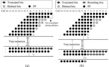
3.1 Deletion, Reduction, and Truncation
In the first step deletion operation is performed, that removes all the avoidable partial product bits which are shown by the light gray dots (fig 2). Delete as many partial product bits as possible in this deletion operation. In Fig. 2, by skipping the first two of partial product bits the deletion of partial product bits starts from
column 3. After the deletion of partial product bits, perform column-by- column reduction of scheme 2.
After the reduction, perform the truncation, which will further removes the first row of (n-1) bits from column 1 to column (n-1). The most significant columns with the variable correction method. It also presents a comparative study of (FPGA) implementation of standard and truncated multipliers using very high speed. Significant reduction in FPGA resources, delay, and power can be achieved using truncated multipliers instead of standard parallel multipliers when the full precision of the standard multiplier is not required.
Fig. 2 8x8 truncated multiplication.(a) deletion, reduction and truncation. (b) Deletion, reduction, truncation, and final addition.
Available online: https://edupediapublications.org/journals/index.php/IJR/ P a g e | 1177 upon the proposed method which reduces delay and
complexity of the process.
The new method for parallel multiplication which computes the products of two n bit numbers by summing only the most significant columns with the variable correction method. It also presents a
comparative study of (FPGA)
implementation of standard and truncated multipliers using very high speed. Significant reduction in FPGA resources, delay, and power can be achieved using truncated multipliers instead of standard parallel multipliers when the full precision of the standard multiplier is not required. We can multiply 8x8 bits, and the bits are reduced in step by step manner in proposed architecture. Deletion is the first operation performed in Stage 1 to remove the PP bits, as long as the magnitude of the total deletion error is no more than 2−P−1. To reduce the final bit width without increasing the error the number of stages are required. In normal truncated multiplier design, the architecture produces the output with some truncation error.
IV.RESULTS
RTL SCHEMATIC
TECHNOLOGY SCHEMATIC
OUTPUT WAVE FORM
V.CONCLUSION
Available online: https://edupediapublications.org/journals/index.php/IJR/ P a g e | 1178
VI.REFERENCES
[1] R. L. Rivest, A. Shamir, and L. Adleman, “A method for obtaining digitalsignatures and public-key cryptosystems,” Commun. ACM, vol. 21, no. 2,pp. 120–126, Feb. 1978.
[2] V. S. Miller, “Use of elliptic curves in cryptography,” in Advances inCryptology. Berlin, Germany: Springer-Verlag, 1986, pp. 417–426.
[3] N. Koblitz, “Elliptic curve cryptosystems,” Math. Comput., vol. 48,no. 177, pp. 203–209, 1987.
[4] P. L. Montgomery, “Modular multiplication without trial division,” Math.Comput., vol. 44, no. 170, pp. 519–521, Apr. 1985.
[5] Y. S. Kim, W. S. Kang, and J. R. Choi, “Asynchronous implementationof 1024-bit modular processor for RSA cryptosystem,” in Proc. 2ndIEEE Asia-Pacific Conf. ASIC, Aug. 2000, pp. 187–190.
[6] V. Bunimov, M. Schimmler, and B. Tolg, “A complexity-effectiveversion of Montgomery’s algorihm,” in Proc. Workshop Complex.Effective Designs, May 2002.
[7] H. Zhengbing, R. M. Al Shboul, and V. P. Shirochin, “An efficientarchitecture of 1024-bits cryptoprocessor for RSA cryptosystem basedon modified Montgomery’s algorithm,” in Proc. 4th IEEE Int. WorkshopIntell. Data Acquisition Adv. Comput. Syst., Sep. 2007, pp. 643–646.
[8] Y.-Y. Zhang, Z. Li, L. Yang, and S.-W. Zhang, “An efficient CSAarchitecture for Montgomery modular multiplication,” MicroprocessorsMicrosyst., vol. 31, no. 7, pp. 456–459, Nov. 2007.
[9] C. McIvor, M. McLoone, and J. V. McCanny, “Modified Montgomerymodular multiplication and RSA exponentiation techniques,” IEE Proc.Comput. Digit. Techn., vol. 151, no. 6, pp. 402–408, Nov. 2004.
[10] S.-R. Kuang, J.-P. Wang, K.-C. Chang, and H.-W. Hsu, “Energy-efficienthigh-throughput Montgomery modular multipliers for RSA cryptosystems,”IEEE Trans. Very Large Scale Integr. (VLSI) Syst., vol. 21, no. 11,pp. 1999–2009, Nov. 2013.
[11] J. C. Neto, A. F. Tenca, and W. V. Ruggiero, “A parallel k-partitionmethod to perform Montgomery multiplication,” in Proc. IEEE Int. Conf.Appl.-Specific Syst., Archit., Processors, Sep. 2011, pp. 251–254. [12] J. Han, S. Wang, W. Huang, Z. Yu, and X. Zeng, “Parallelization ofradix-2 Montgomery multiplication on multicore platform,” IEEE Trans.Very Large Scale Integr. (VLSI) Syst., vol. 21, no. 12, pp. 2325–2330,
Dec. 2013.
[13] P. Amberg, N. Pinckney, and D. M. Harris, “Parallel high-radixMontgomery multipliers,” in Proc. 42nd Asilomar Conf. Signals, Syst.,Comput., Oct. 2008, pp. 772–776.
[14] G. Sassaw, C. J. Jimenez, and M. Valencia, “High radix implementationof Montgomery multipliers with CSA,” in Proc. Int. Conf. Microelectron.,Dec. 2010, pp. 315–318.
[15] A. Miyamoto, N. Homma, T. Aoki, and A. Satoh, “Systematicdesign of RSA processors based on high-radix Montgomery multipliers,”IEEE Trans. Very Large Scale Integr. (VLSI) Syst., vol. 19, no. 7,pp. 1136– 1146, Jul. 2011.
PINAPATI JAYALAKSHMI studied at B.Tech Don Bosco institute
of technology and science during 2009-2013 present she is pursuing M.Tech at mallineni lakshmaiah women’s engineering college. Her area of interested VLSI design.
KADULLA HARIBABU Studied B.Tech at QIS College of