ABSTRACT
SRINIVASAN, VINESH. Phase II Implementation and Verification of the H3 Processor. (Under the direction of Dr.Eric Rotenberg).
With the 2D version of the H3 processor from phase I tapeout well into post silicon debug, this thesis effort focuses on the implementation of 3D version for the phase II tapeout. The main focus is on fixing the bugs identified in the phase I chip, netlist simulation based verification effort to identify new bugs and fixing them.
In addition to the 3D restructuring of the chip from Phase I tapeout, some new features have also been implemented for the 3D tapeout, which are also an integral part of this thesis. This includes, a new data cache that has been integrated to replace the OpenSparc T2 data cache from the phase I tapeout, virtual memory support for not flushing caches on migration and an invalidation based cache coherence mechanism in order to avoid the threads hitting on its own stale data after migration. In addition to the existing design, these new features are also extensively tested for corner cases.
Phase II Implementation and Verification of the H3 Processor
by
Vinesh Srinivasan
A thesis submitted to the Graduate Faculty of North Carolina State University
in partial fulfillment of the requirements for the degree of
Master of Science
Computer Engineering
Raleigh, North Carolina 2015
APPROVED BY:
_______________________________ _______________________________
Dr.Eric Rotenberg Dr.W.Rhett Davis
Committee Chair
DEDICATION
BIOGRAPHY
ACKNOWLEDGMENTS
Thanks to my advisor, Dr. Eric Rotenberg for his support and guidance right from the start of my time at NC State. I also want to thank him for advising me throughout the course of this year-long project. His commitment to achieve perfection both as a teacher and a researcher is inspiring. I immensely benefitted both from his classes and our research discussions at his office. I would like to thank Dr. James Tuck and Dr. Rhett Davis for agreeing to serve on my thesis committee and their valuable feedback.
Thanks to Rangeen and Anil, for helping me initially to get accustomed to the tools and infrastructure needed for research. Their valuable inputs and discussions helped me throughout the course of this thesis. I also would like to thank Elliott for his guidance related to this project. Without their help this thesis would not be possible. I enjoyed all the fun discussions with Anil which made our time at the lab memorable. I would like to thank Naren and Raghav for all their help, the driving classes, cooking recipes and more which made my life at Raleigh enjoyable.
Thanks to my dad Srinivasan and mom Vijayavalli as they gave me the freedom to make my own decisions and are always supportive no matter what I do. I am forever grateful to them for the sacrifices that they make in order to make my life better. I also would like to thank my little brother, Harish for always being there for me. Finally, I would like to thank Srividhya for her unconditional love and support to my decisions.
TABLE OF CONTENTS
LIST OF TABLES ... vii
LIST OF FIGURES ... viii
Chapter 1 INTRODUCTION ... 1
1.1 H3 - 3D Heterogeneous Multicore Processor ... 1
1.2 H3 Tapeout: Phase I (2D version) ... 5
1.3 H3 Tapeout: Phase II (3D version) ... 5
1.4 Contributions for Phase II ... 8
1.4.1 Bug Fixes ... 8
1.4.2 New Features ... 9
1.4.3 Verification ... 10
Chapter 2 BUG FIXES ... 12
2.1 Load Wakeup Bug ... 12
2.2 T2 D-cache Bug ... 14
2.3 False BTB hit Bug ... 15
2.4 CTIQ Full Bug... 17
2.5 CCD Bug ... 18
2.6 CTIQ Performance Bug ... 19
2.7 Netlist Simulation ... 20
Chapter 3 NEW FEATURES ... 22
3.1 Data Cache ... 22
3.3 Cache Coherence ... 26
Chapter 4 VERIFICATION ... 28
4.1 Stress Tests for Bugs and Fixes... 28
2.1 Load Wakeup Test ... 28
2.2 Data cache Test ... 30
2.3 False BTB Hit Test ... 34
2.4 CTIQ Full Test ... 36
2.5 CCD Test... 38
4.2 Stress Tests for New Features ... 40
4.2.1 Cache Coherence ... 41
4.2.2 Virtual Memory ... 45
4.2.3 Configuration Pins ... 47
4.2.4 Performance Counters... 49
4.2.5 Wave Instruction ... 50
4.3 Performance Tests ... 51
4.3.1 FTM Latency ... 52
4.3.2 CCD Performance ... 54
4.3.2 Not-Flushing-Caches Performance ... 57
4.4 Benchmark Results ... 57
Chapter 5 SUMMARY ... 60
LIST OF TABLES
Table 4.1 Load wakeup stress test measurements ... 29
Table 4.2 Data Cache stress test measurements ... 31
Table 4.3 Data cache Load/store size stress test measurements ... 33
Table 4.4 False BTB hits stress test measurements ... 35
Table 4.5 CTIQ fill stress test measurements ... 37
Table 4.6 CCD stress test clock relations ... 40
Table 4.7 Invalidations Test counters ... 43
Table 4.8 Virtual Memory Test counters ... 46
Table 4.9 Flush caches enabled test counters ... 48
Table 4.10 CCD enabled test counters ... 48
LIST OF FIGURES
Figure 1.1 Fast Thread Migration Design in H3 ... 3
Figure 1.2 Cache Core Decoupling design in H3 ... 4
Figure 1.3: H3 Phase II design block diagram ... 7
Figure 2.1 Waveform showing the hold time violation in T2 Data Cache ... 14
Figure 2.2 Waveform showing the CCD Bug ... 18
Figure 3.1 Top level organization of the L1 Caches-Memory Interface in H3 ... 24
Figure 3.2 Virtual to physical address translation and memory interface in H3 ... 25
Figure 3.3 Cache Coherence Design in H3 ... 27
Figure 4.1 Load wakeup stress test ... 29
Figure 4.2: Data cache stress test ... 30
Figure 4.3 Store buffer size stress test ... 33
Figure 4.4 False BTB hit stress test ... 35
Figure 4.5 CTIQ full Stress Test ... 37
Figure 4.6 CCD Stress Test ... 39
Figure 4.7 Invalidation logic stress test ... 42
Figure 4.8 Invalidation request vs. FTM latency ... 45
Figure 4.9 Performance counters Test ... 51
Figure 4.10 Waveform for the wave test ... 51
Figure 4.11 Test for FTM latency measurement ... 53
Figure 4.12 FTM latency measurements ... 54
CHAPTER 1
INTRODUCTION
The instruction level parallelism (ILP) inherent in different programs and different phases of the same program varies. Thus the need to design diverse microarchitectures each specialized to suit different program phases arises. Microarchitectural diversity is of three types:
1. Single-ISA heterogeneous multicore processor where each core may differ in their superscalar structure dimensions and/or frequency.
2. Adaptive superscalar processor which is a single reconfigurable core 3. CPU + accelerators (ASICs, FPGA, GPGPUs)
1.1 H3 - 3D heterogeneous multicore processor
The H3 processor comes under the class of single-ISA heterogeneous multicore processor. H3 is a dual-core processor implemented using 3D die stacking where both the cores are integrated by face-to-face, microbump based buses. It consists of two core types named based on their peak instruction fetch rate. Two-wide OOO core, a high performance core that has bigger superscalar structure sizes to extract more ILP from the running program and a one-wide OOO core, a low power core that has smaller structure sizes more suitable for phases that less exploits the performance benefit of the big core. The rationale behind running on the little core is to reduce energy consumption with only a small slowdown compared to always running on the big core [1].
closer to the big core. But, fine grained thread migrations are more sensitive to migration overheads as the opportunity to exploit the short phases is lost if the overhead is high. Migration overheads come from the following two sources:
1. Transferring architectural register state: Architectural register state includes the architectural registers, program counter etc. The latency for transferring the architectural register state from the source core to the destination core is a major source of migration overhead.
2. Migration induced misses and mispredictions: After migration, if the core misses a cache block that exist in the previous cache but not in the current cache it is called a migration induced miss. This can occur due to two reasons.
i) If there are two threads running, then one thread can evict blocks that might be useful for the other thread after migration.
ii) Stores on the other core can cause invalidations in the current core.
Other speculative structures like the branch predictor need time to get trained as counter values can be evicted by the other thread. Migration induced cache misses include these extra misses incurred.
3D die stacking enables fine grained thread migration by overcoming these migration induced overheads [1]. H3 handles these migration induced overheads via two mechanisms, they are:
Fast Thread Migration (FTM):
one core to the other. It is made possible by using a dedicated structure that holds the architectural register state called the “Teleport Register File” (TRF) and face-to-face buses that connect each bitcell of the TRF to the other core’s TRF as shown in figure 1.1.
Figure 1.1 Fast Thread Migration Design in H3 [3]
The TRF registers, F2F logic are in a separate module called F2F control which also has the core suspend and resume handshaking. Although the swap can occur in one cycle, the cores require some cycles for consolidating the architectural register state from the Physical Register File (PRF) to the TRF using special instructions that does the move from the PRF to the TRF and vice versa. Along with the register values, the program counter is also moved to the TRF. Including consolidation, FTM has around 100 cycle latency for transferring architectural register state from one core to the other.
Two types of migrations can occur in the H3 design:
2. Local Migrations: Software-triggered migrations by embedding the migrate instruction along with the program code, which is executed by the processor.
Cache Core Decoupling (CCD):
Cache Core Decoupling (CCD) tries to reduce the overhead caused by migration induced cache misses. CCD enables each core to access the other core’s L1 instruction and data cache. Figure 1.2 shows the CCD logic located at the fetch and memory state of the pipeline that connects each core to the other core’s instruction and data caches respectively. This enables the threads to freely migrate from one core to another without having to switch caches. There can be different modes of operation with CCD. The threads can be mapped to the best core, cache throughout its execution. Or, the threads can choose to migrate cores but not caches thus avoiding migration induced cache misses.
1.2 H3 Tapeout: Phase I (2D version)
Phase I of H3 involved building a 2D version of the two-core-stack. The 2D version is mainly to test the design which included the FabScalar generated cores with compiled memories for instruction and data cache, FTM, CCD implementations, and also to work out the physical design flow. In addition to the two-core-stack, the phase I design also included a two-wide debug core. The debug core had synthesized scratchpads for instructions & data and full scan. The purpose of designing the debug core is to test the core without risks caused by the synthesized RAMs, and the highly complex OpenSparc T2 D$ which the two-core-stack was using. The phase I design was taped out on May 2013. The tapeout was done using IBM 8RF (130 nm) PDK and ARM standard cells, pads and memory compilers.
Post-silicon Tasks:
The debug core which was tested using a chip-on-board setup was successful in performing the liveness test and went onto retire millions of instructions of microbenchmarks. The two-core-stack in its Quad Flat Package was surface mounted onto the 4-layer PCB. The PCB was connected to Xilinx ML605 FPGA board as a mezzanine card using an LPC connector. The testbench, which also acted as L2 for servicing L1 instruction and data cache misses was synthesized to the FPGA. With this setup in place, more bugs were discovered in the chip during post-silicon debug process which are documented in detail in the WARP submission [2]. Chapter 2 describe the fixes that are made for each of these bugs in detail.
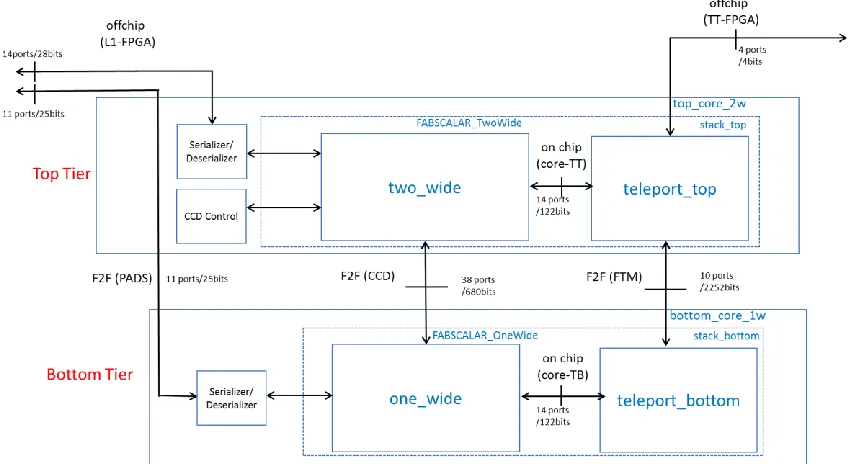
1.3 H3 Tapeout: Phase II (3D Version)
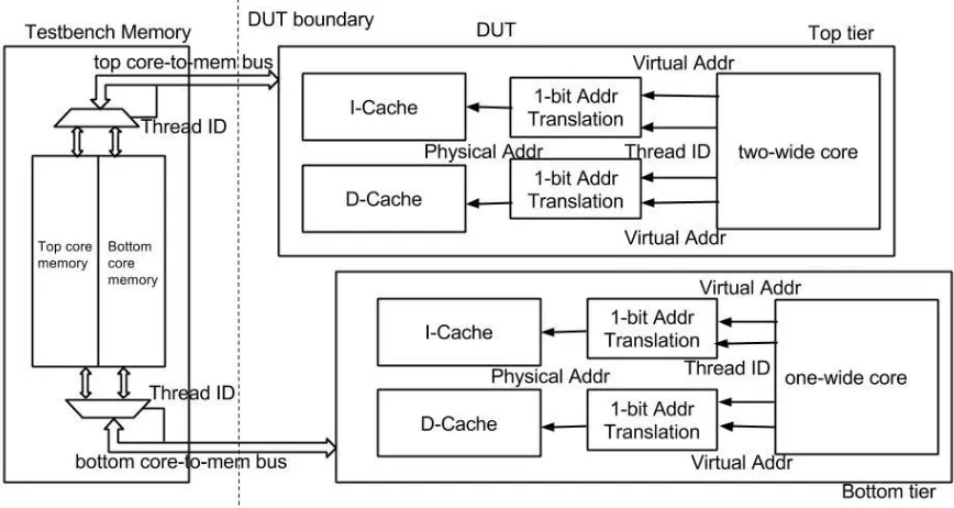
identifying and fixing newer bugs, implementing newer features that did not make it into the phase I tapeout, all of which is documented in this thesis. In phase II, the two chips are vertically stacked and bonded with face-to-face microbump based buses. Conventional top metal layer pads cannot be used because the two chips are bonded to each other. Hence, we are planning to use Ziptronix 3D process of implementing pads on the metal 1 layer of the top (flipped) chip. The pads are exposed by thinning the upper chip’s substrate and back-etching through the substrate to reach the pads. The chip will then be wirebonded on to the package. Since the top chip has all the pads allotted for the two-core-stack, the bottom core needs to route its I/O through the top core to reach to the pads.
Figure 1.3 shows the arrangement of the two-core-stack, the two-wide core and its corresponding FTM logic (Teleport top) is located in the top tier, the one-wide core and its FTM logic (Teleport bottom) is located in the bottom tier. The teleport units in both the cores interact using the F2F-FTM bus interface, which is as wide as the TRF registers in the cores to enable single cycle data transfer. CCD control orchestrates the core-cache mapping for both the cores. It’s a separate control module that handshakes with the suspend and resume
Figure 1.3: H3 Phase II design block diagram
1.4 Contributions for Phase II:
This section briefly outlines my contributions made for the Phase II tapeout that are discussed in detail in the future chapters in this thesis.
1.4.1 Bug Fixes:
1. Post-Silicon phase I bugs & fixes: The post-silicon bugs identified during the phase I tapeout is documented in detail along with their fixes. Some of the bugs which we were able to reproduce in RTL simulations were reproduced and fixed. Netlist simulation was used to fix the rest of the bugs.
T2 Data Cache Bug: One among the critical bugs identified during netlist simulation was the Opensparc T2 data cache bug. The T2 design explicitly used latch based indexing for its tag and data RAMs. On a load fill, due to hold violation in the address latch the tag RAM was not written. In addition, the use of latches for indexing was found in other parts of the design including the store buffer. Thus we decided to replace the T2 data cache with an in-house designed data cache. The efforts related to the new data cache integration are outlined in the new features section.
1.4.2 New Features:
1. 3D Restructuring: After phase I tapeout, the restructuring for phase II involved, splitting the top level module of the 2D structure into top and bottom tiers, moving the common logic related to the CCD control to the top tier. More effort was spent on modifying the I/O for the bottom tier to face-to-face buses and routing them through the top tier to reach to the pads. The complexity arises mainly from the huge number of F2F signals. The different classes of F2F signals are FTM, CCD and pads.
2. I/O Classification and Routing: Each class of I/O, interfaces to a different module in each tier hence needed careful classification and routing compared to the 2D design. The F2F buses were annotated to differentiate them from the I/O to ease physical design process of routing the F2F signals to the face-to-face microbump based buses and I/O to pads.
3. New Data Cache Integration: One of the major changes in the phase II design over phase I is the new data cache. The T2 data cache used compiled RAMs hence the pipeline was modified to suit the synchronous read/writes. The new data cache with its memory synthesized to flip-flops has asynchronous reads and synchronous writes. The pipeline had to be modified to accommodate this change. Further, the T2 data cache arbitrated load and store requests to the memory internally which eased top level design in the phase I tapeout. Arbitration had to be done at the top level module for phase II as the new data cache did not do the load/store request arbitration internally.
environment hence there is no memory sharing as in a multithreading environment. The caches in the phase I tapeout were virtually indexed and virtually tagged and during a migration caches were always flushed as the other program’s address space is different. The L2 always maps the cache to the correct address space after migrations. This was easy to implement as it did not require any virtual-physical memory translation.
For the phase II tapeout, the caches are made virtually indexed but physically tagged this enables us to not flush caches during migrations. The virtual to physical translation is a 1-bit thread-id that maps the cache block to its corresponding address space in the memory.
5. Cache Coherence: Although there is no memory sharing, when we are not flushing caches, cache coherency among the caches is still required because a thread can load a data from memory, migrate from one core to the other, commit to the same memory, migrate back and will receive a stale data. An invalidation based cache coherency protocol has been implemented to avoid this scenario in phase II. It required changes to the L2 for monitoring the tag banks of the caches to generate invalidations and also to the data cache to receive these invalidations and act upon them.
1.4.3 Verification:
The verification effort consists of different classes of test cases. Each of the classes focus on testing different aspects of the design. The tests are classified as:
2. Stress test for new features: Tests for the new features include tests for the new data cache, virtual memory and cache coherence support. Also, new bugs found during these stress tests and their fixes are discussed in detail.
3. Performance tests: These tests are to measure the performance of novel aspects of the phase II H3 design. Tests designed for measuring the FTM latency, CCD benefits, not flushing caches benefits were executed to make sure they match with the expected performance from the chip. These test strategies along with the results is discussed in detail. 4. SPEC benchmarks: Commercial workloads were run on the design to show the real world application of the H3 processor and graphs showing these performance results are shown and discussed.
CHAPTER 2
BUG FIXES
A comprehensive list of bugs found in H3 phase I and their work-around are presented in the WARP submission [2]. This chapter explains in detail some of the bugs in the design found in the post-silicon debug process of the phase I chip that are fixed as part of this thesis’s efforts. Some of the bugs which were reproducible in RTL simulations were fixed. Other bugs were investigated using netlist simulation and fixed. This chapter will also discuss the netlist simulation process in detail and how it was useful in investigating bugs that was observed on the chip but not in RTL simulations.
2.1 Load Wakeup Bug:
Bug Description: Load wakeup bug was caused by a misplaced `ifdef in the RTL which was exercised only in simulation and not during synthesis. In the fabscalar pipeline, once a load is issued for execution, its writeback packet is created with information related to the load i.e. its destination register ID, Activelist ID etc. The valid bit of the packet is set based on both the load’s validity and data valid that comes after the load has hit in the cache. For a load that
misses in the cache, its writeback packet consists of all information about the load with its valid bit set as ‘0’.
issue stage wake-up mechanism for invalid bypass packets, as all instructions can be checked only for a match with the register tags and not the valid bit of the bypass packet. This crucial part of packing the bypass packet with P0 was inside the `ifdef, which got omitted during synthesis. So despite the bypass packet not being valid the register tags from the writeback packet was broadcasted, thus causing early wakeup of the load dependent instruction that already reached the issue queue. Although, future instructions that are just getting renamed get their ready bits from the PRF, once they reach the issue queue, matches with the register tag every time the load replays thus causing early wakeups throughout the load’s
miss penalty.
Fix: There are two fixes that are made to ensure that the bug is fixed.
1. First is removing the misplaced `ifdef from the RTL to make sure that the netlist and RTL simulation matches. All other instrumentations were also removed to make sure that the RTL simulation was not running based on any instrumentation that will not be used in synthesis. This ensures that the bypass packet wakeup tags were filled with P0.
2.2 T2 D-Cache Bug:
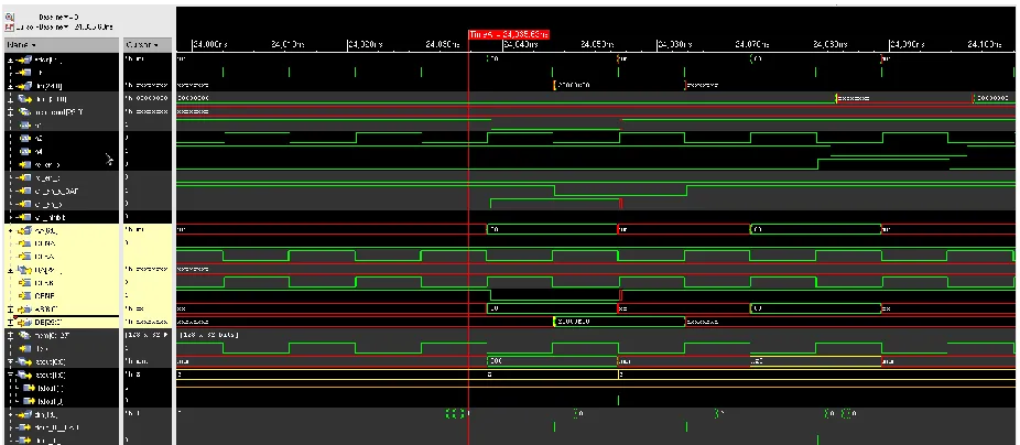
Figure 2.1 Waveform showing the hold time violation in T2 Data Cache
Bug Description: The T2 data cache used for the phase I tapeout had compiled RAMs for tag and data banks. Whenever a load misses in the cache, a request is sent to the memory and when the fill arrives, the tag bank needs to be written. The T2 data cache uses a highly custom latch based design for writing RAMs. The index/address gets latched into a positive level sensitive latch and the tag goes through a flip flop. Both the edges of the clock are used to write into the RAMs.
The waveform figure 2.1 shows the output of the latch “latout” for the address and “din” shows the data to be written into the tag RAM. The I/O of the tag RAM is highlighted
DB belongs to the write port of the RAM. The CLKB signal is a 180-degree phase shifted version of CLKA. The positive level of CLKA is used to latch the address, enable which is shown as input AB, CENB (active low) to the RAM. The next posedge of CLKA is used to latch the data which is input DB to the RAM. The RAM is expected to get written on the posedge of CLKB. But due to hold violations at the latch, the address AB becomes ‘x’ before the posedge of CLKB causing the fill to be incomplete. The output of the RAM QA is shown.
Fix: This style of using latched to write the RAMs were found prevalently in other places of the design including the data RAM and store buffer write logic. In addition, the highly structured design of the T2 data cache made debugging difficult. Hence to fix this issue, the T2 data cache was replaced with an in-house developed data cache. The efforts related to replacing the data cache are described in detail in Chapter 3. Chapter 4 discusses stress cases run on the new data cache to make sure other problems related to the data cache do not surface in phase II.
2.3 False BTB hit bug:
immediate is compared with the BTB taken PC and branch type. If it fails to match, then it is considered as a BTB miss even though it hit in the BTB, thus forcing recovery in case of predicted taken branches. In case of other instruction types hitting in the stale data, their opcodes are used at predecode to generate a false BTB hit signal that forces recovery. As both BTB miss and false BTB hits forces recovery, they were handled in a similar manner in the fetch stage 2. Fetch stage 2 also handles allocating CTIQ slots for control instructions which will be updated later when they execute. Since instructions that generate BTB misses are genuine branches they were allocated CTIQ entries. Erroneously, the same logic was applied for false BTB hits causing wrong allocation of CTIQ entries. This resulted in wasted CTIQ entries as the instructions that false BTB hits will never clear their CTIQ entry. Eventually, core runs out of CTIQ entries and deadlocks.
2.4 CTIQ Full Bug:
Bug Description: The local migrate instruction that is executed along with the program code at retirement, triggers the FTM logic for state transfer. Once the migration flag goes high, the fetch stage is stalled to make sure no further instructions are fetched. But at the intermediate time between fetch and retirement of the migrate instruction, the pipeline fetches past the migrate instruction that alters the pipeline stages that is not squashed during migrate. One such stage is the CTIQ allocation stage, where new control instructions, when fetched are allocated CTIQ entry that are later cleared after execution. But control instructions that are fetched past the migrate instruction, only gets allocated CTIQ entries and are not cleared. As the thread keeps migrating from one core to the other, there is a lost CTIQ entry for every migration. Eventually, after the thread has migrated 32 times the CTIQ, which is sized at 16 entries for the two-wide core, gets filled up. And at the 33rd migration the core stalls as CTIQ is full.
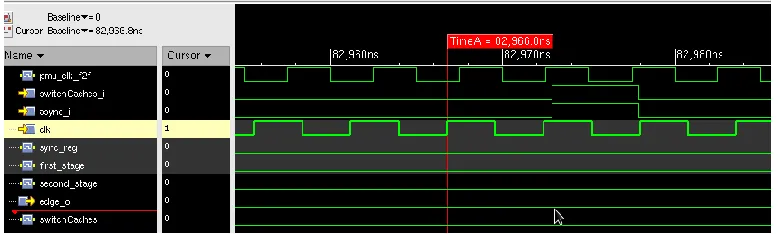
2.5 CCD Bug:
Figure 2.2 Waveform showing the CCD Bug
Bug Description: The CCD control state machine is responsible for the select signal to the muxes that maps the core either to the remote or to the local caches when CCD is enabled. They work based on the F2F clocks as the logic is common to both the cores. During first migration, the barrier signal from the cores reaches the control state machine which indicates that the cores have stalled fetch and are ready for migration. Once barrier signals of both cores are high, the “switch_caches” pulse is sent, which is latched by the cores. The F2F
controller on seeing the barrier does the architectural register state transfer and sends the resume signal to the state machine. This resume is received by the CCD state machine and sent few cycles after the “switch_caches” pulse to ensure that the core cache mapping is complete. Based on the switch caches signal and external CCD configuration pin, cores get mapped to one of the caches.
slow clock domain is missed by the double flip-flop synchronizer causing wrong core-cache mapping. Thus, CCD will fail after an arbitrary number of migrations. Figure 2.2 shows one such instance where the incoming pulse is missed by the double flip-flop synchronizer. Fix: The CCD control logic was organized by having all the clock domain crossing signals into a single module. The “switch_caches” signal logic which was earlier generating a pulse is now changed to a control signal that is high after the first migration and throughout the phase during which threads can access the remote cache. This way, the signal will not be missed by the cores and based on the CCD configuration pin the cores can choose to make the core access the remote caches. All signals that crosses clock domains are tested for various core-F2F clock combinations to ensure this bug do not appear in phase II. The test is shown in Chapter 4.
2.6 CTIQ Performance Bug:
Bug Description: After a branch is predicted, its predicted direction, prediction counters is packetized along with the instruction to fetch stage 2. In fetch stage 2 all control instructions are allocated CTIQ entries. During allocation, the branch’s prediction counter is also written
in the CTIQ. Later, when the branch executes, its next PC, control type, the actual direction taken is written into the entry allotted. Once execution is complete, the branch’s prediction
counters allocated earlier, are now updated with the actual direction taken and then written to the branch predictor’s counter table. Whenever CTIQ is full the tail points to the head entry
instruction got written into this head entry, thus causing wrong counter updates to the branch predictor.
Fix: The control vector input signal to the CTIQ shows how many control instructions are in the current fetch bundle that require a CTIQ entry. This control vector was previously used as the write enable to the CTIQ prediction counter RAM. This is now fixed by qualifying the input control vector with the CTIQ full signal. When CTIQ is full the write enable to the RAM is disabled. And only when CTIQ is not full, the input control vector directly acts as write enable to the counter RAM.
2.7 Netlist Simulation:
its corresponding SDF, the names of all the modules across both the tiers were uniquified during synthesis.
CHAPTER 3
NEW FEATURES
This chapter discuss the new features that are added to phase II design that did not make it into the phase I tapeout. The major changes made to the design are, the replacement of the T2 data cache with the new data cache, support for virtual memory to not flush caches and cache coherency support. These three changes are discussed in detail in this chapter and the verification effort of these new changes is discussed in Chapter 4.
3.1 Data Cache:
The bugs found with the T2 data cache and the reason for replacing it is discussed in detail in chapter 2. This section discusses the new data cache and the related efforts in integrating them to the two-core-stack design.
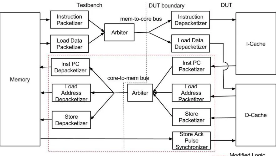
The new data cache is a 2KB, direct mapped cache. It supports hit under miss and it has one MSHR, hence capable of handling one outstanding miss at a time. The cache is a write-through cache, hence store requests on commit goes to the memory first before updating the cache. Only after the store acknowledgement returns to the cache, and if the store hits, it is updated in the cache. The major difference between the new data cache and T2 is the asynchronous read, synchronous write interface of the new data cache over synchronous read/write of the T2. The new data cache is designed for the tag and data banks to be synthesized to flip flops instead of RAMs as it was with T2.
unit. This was done to make the output of the Agen directly feed the data cache and the Agen-LSU pipeline register. So that, the 2 cycle latency of the data cache matches with the rest of the logic related to store queue accessing, load violation detection logic etc. These changes to the pipeline are now modified to make the output of the Agen-LSU feed both the dcache and store queue as the dcache output comes at the same cycle as the request. Similarly, other logic related to store queue match and writeback are adjusted for the new data cache.
In addition to the changes in the pipeline, the new data cache required arbitration between the load and store requests going to the memory. The T2 data cache arbitrated these requests internally hence making top level arbitration between instruction and data cache request for the single 8-bit core-to-mem bus easier. Now, there are 3 clients for the top level arbiter. They are I-cache, load, and store requests. The arbitration at the core side was made complicated as the packets should not only be arbitrated for a single bus but also should be differentiated from one another at the memory side depacketizer. This is achieved by using the packet ids of the packetizers.
Figure 3.1 Top level organization of the L1 Caches-Memory Interface in H3
3.2 Virtual Memory:
core has to start off with cold data caches when it migrates to the core again but also that it loses its instruction cache contents which if not flushed can save on crucial I-cache misses.
In order to not flush caches, the cores need to be aware of its physical memory space; hence a virtual to physical address translation is necessary. Since at most we can have only two programs running on the H3 processor, the virtual to physical memory mapping is a one-bit thread ID. This translation from virtual to physical address happens during cache access where the uppermost bit of the tag is embedded with the thread ID. Thus, the caches are made virtually indexed but physically tagged. This way there is no need to flush the caches when programs migrate and also the requests to the memory have the thread ID embedded in them, thus no external signal is necessary to map the block to the physical address location.
Figure 3.2 shows the two cores and their virtual to physical address translation methodology. The caches use physical address for tags and thus based on the thread ID, the packet can be demuxed to one-half of the memory. The program can freely migrate from one core to the other without the need for flushing caches.
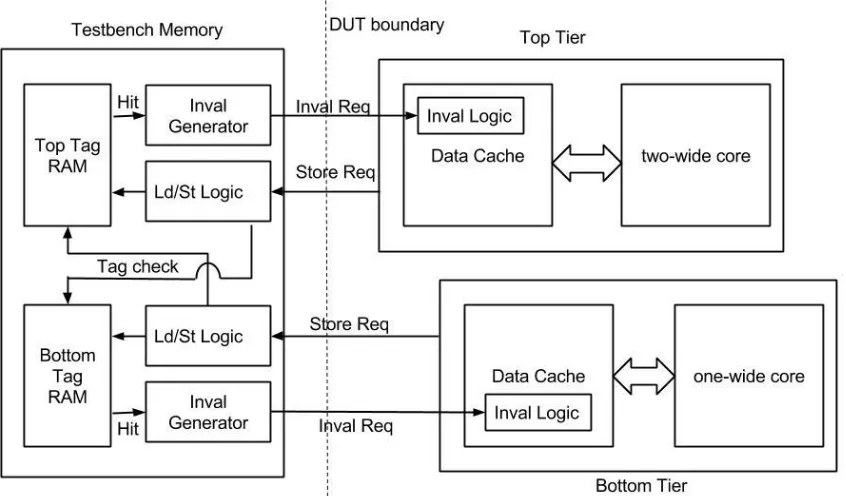
3.3 Cache Coherence:
Virtual memory ensures that when a new program migrates to a core it will not hit on the old program’s cache contents thereby enabling not flushing caches. But not flushing caches can
Figure 3.3 Cache Coherence Design in H3
The cache coherency model not only requires book-keeping at the memory level but also the data caches should be equipped with invalidation request detection logic. This logic is shown in the figure as the “Inval logic” inside the data cache. Whenever a data cache sends a store request to the memory, the store logic accepts the store request and then sends the store address to the other core’s tag RAM via the tag check interface. If it detects a hit, then the “Inval generator” uses the address to send an invalid request to the data cache and invalidates
CHAPTER 4
VERIFICATION
The verification effort related to phase II covers the following: 1. Stress tests for bugs found during phase I and its fixes 2. Tests for new features that are implemented in phase II
3. Performance tests for novel features related to FTM, CCD and not flushing caches 4. SPEC and microbenchmark results
All the tests used in this chapter are written and compiled using “Duct-Tape” an in-house
developed assembly compiler. Each class of test cases are explained in detail with the test run, coverage counters and bugs found in the following sections.
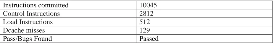
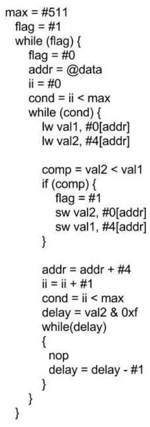
4.1 Stress Test for Bugs and Fixes: 4.1.1 Load Wakeup Test:
random dependency chains. This will create a varying number of load-dependent instructions that reach the issue queue at different cycles. Every time the load replays and misses the register tag needs to use the P0 tag for not waking up dependents. Hence, both the PRF ready bits and register tags during load replays are verified. The test used and the counts regarding the test is shown in the figure and Table 4.1 respectively.
Figure 4.1 Load wakeup stress test
Table 4.1 Load wakeup stress test measurements
Instructions committed 10045
Control Instructions 2812
Load Instructions 512
Dcache misses 129
4.1.2 Data Cache Test:
Table 4.2 Data Cache stress test measurements
Instructions committed 8980400
Load Instructions 524286
Store Instructions 261633
Data Cache miss 1152
Store Queue Hits 76089
Store Buffer Hits 107575
Pass/Bugs Found Passed
Store Buffer Size Bug:
Previous test checks only loads and stores that have the same sizes. While running load stores with different sizes a bug was found which is described in this section. The bug was found when we load a particular word, store a new word to the same address and load a byte from the same address. The load byte was getting the old value from the cache instead of getting the new store value. This bug occurred because the store-load forwarding mechanism in the fabscalar pipeline is conservative by not forwarding value for loads that do not match the store’s size. Instead, these loads are considered violated and are made to replay. When the
replay happens, the store reaches the store buffers. The store buffers do not check for partial matches and hence the load gets the stale value from the cache. This is now fixed by
Figure 4.3 Store buffer size stress test
Table 4.3 Data cache load/store size stress test measurements
Instructions committed 19119
Load Instructions 3072
Store Instructions 512
Data Cache miss 129
Load Violations 23
The test creates the same scenario that caused the bug and also the internal delay loop changes the time at which the load bytes reach the cache. Thus some of them may end up as load violations which are indicated in the table, other loads might reach the store buffer but will be made to replay and get the data after the store completes. The alternate case when there is a store to a byte and load to a word is also addressed using the same method of cancelling the load’s hit was also verified.
4.1.3 False BTB hit Test:
Figure 4.4 False BTB hit stress test
Table 4.4 False BTB hits stress test measurements
Instructions committed 67108927
Control Instructions 4194305
False BTB hits 62914589
The program executes close to 67 million instructions out of which 63 million instructions are non CTI instructions that wrongly hit in the BTB, hence are tagged as false BTB hits. Other control instructions come to around 4 million. The test passed generating the correct final seed value.
4.1.4 CTIQ full Test:
Figure 4.5 CTIQ full Stress Test
Table 4.5 CTIQ full stress test measurements
Instructions committed 210079
Control Instructions 20002
Migrations 10000
4.1.5 CCD Test:
Table 4.6 CCD stress test clock relations
Core clock period (ns) F2F clock period (ns) Pass/Fail
10 10 Pass
12 10 Pass
14 10 Pass
15 10 Pass
20 10 Pass
25 10 Pass
30 10 Pass
10 12 Pass
10 14 Pass
10 15 Pass
10 20 Pass
10 25 Pass
10 30 Pass
4.2 Stress Test for New Features:
4.2.1 Cache coherence:
Table 4.7 Invalidations Test counters
Top Core Load Instructions 262654
Top Core Store Instructions 131073
Top Core Data Cache miss 209965
Top Core Invalidations 81279
Bottom Core Load Instructions 261632
Bottom Core Store Instructions 130560
Bottom Core Data Cache miss 81921
Bottom Core Invalidations 81283
Pass/Bugs Found Passed
This test initially revealed an interesting bug related to lost invalidation requests from the memory. As we discussed in one of the previous sections, the resume signal after migration resets most of the structures in order to restore the destination core to a pristine state before resuming execution. This resume signal was also resetting the depacketizer modules that are responsible for receiving the load fill/invalidations from the memory. This resulted in lost invalidations which caused the loads to hit on the stale data in the caches. This can also cause problems when CCD is enabled as load fills can be dropped by the depacketizer causing miss handling structures inside the data cache that are waiting for the response to create deadlock scenarios. Hence, this was fixed by not resetting the depacketizer when flush is disabled or CCD is enabled.
to wait for the invalidations before migration due to performance reasons; the migrate can happen once the final store has been acknowledged by the memory. This can create problems when the invalidations are delayed and fails to reach the core before the first cache access; hence it creates a thread synchronization problem as the threads need to synchronize with its own requests reaching the other core before migrations. In case of global migrations, this risk is reduced as the migration penalty which comes mainly from moving the architectural register state that is all 34 registers, and the PC to the other core is high which gives plenty of time for the invalidations to reach the other core before the thread migrates. In case of local migrations which are software triggered migrations, the migration latency can be less. As the software knows the number of registers to be moved and hence can reduce the time taken for architectural register state transfer. This study was done to identify the least amount of registers needed to be transferred for which the invalidations will reach the destination core safely before the thread does. The test used for this study is shown in figure 4.8.
this study the memory is assumed to be clocked at the same rate as the cores. If this clock relation is changed, by making the memory slower the test fails, thus showing the breaking point up to which we can be assured of the invalidations reaching the cores before the loads.
Figure 4.8 Invalidation request vs. FTM latency
4.2.2 Virtual Memory:
Virtual memory implementation can be tested by running two threads simultaneously on the two-core-stack without flushing the caches. This creates scenarios where the memory blocks from both the threads co-exist in the caches and the translation methodology should ensure that one thread does not hit on the other thread’s memory block. This theory is tested by
global migrations. The threads migrate after a fixed time interval specified by an external counter, which is now set at 16K cycles for this test, without flushing its caches and should successfully complete thus ensuring that the memory space for both the threads has been handled properly. The run successfully completed committing 400K instructions from bzip and 300K instructions in vortex. Table 4.8 shows the measurements from the run.
Table 4.8 Virtual Memory Test counters
Top core committed instructions 409503
Top core control instructions 84210
Top core ld instructions 112766
Top core st instructions 33245
Top core dc miss 6641
Top core ic miss 6148
Top core invalidations 508
Bottom core committed instructions 366180
Bottom core control instructions 74322
Bottom core ld instructions 97338
Bottom core st instructions 31105
Bottom core dc miss 5647
Bottom core ic miss 5832
4.2.3 Configuration Pins:
Table 4.9 flush caches enabled test counters
Top core committed instructions 431907
Top core control instructions 88452
Top core ld instructions 117125
Top core st instructions 34912
Top core invalidations 0
Bottom core committed instructions 382028
Bottom core control instructions 76987
Bottom core ld instructions 99954
Bottom core st instructions 33397
Bottom core invalidations 0
Table 4.10 CCD enabled Test counters
Top core committed instructions 410048
Top core control instructions 84273
Top core ld instructions 112340
Top core st instructions 33275
Top core invalidations 0
Bottom core committed instructions 380070
Bottom core control instructions 77107
Bottom core ld instructions 100796
Bottom core st instructions 32827
The table 4.9 lists measurements when the two threads are run with CCD disabled and flush caches enabled. In this case both the caches are flushed on a migrate by both the threads hence there are zero invalidations generated. Similarly table 4.10 lists measurements for CCD enabled, which also shows zero invalidations as the same caches are accessed by the threads throughout the run. This ensures correctness of the configuration pins.
4.2.4 Performance Counters:
Table 4.11 Performance Counter measurements
Instructions committed 3152
Control Instructions 514
Load Instructions 512
Store Instructions 1
Mispredictions 3
Data Cache miss 129
Instruction Cache misses 25
Load Violations 0
Issue Queue full 0
Active List full 3745
Load queue full 0
Store Queue full 0
Instruction buffer full 3222
Pass/Bugs Found Passed
4.2.5 Wave Instruction:
Figure 4.9 Performance counters Test
Figure 4.10 Waveform for the wave test
4.3 Performance Tests:
4.3.1 Fast Thread Migration Latency
The feature to perform thread migrations with reduced latency is one of the novel features of H3. This feature is measured here with the help of a test case and its results are discussed. The test makes use of the wave instruction as a method of communicating the completion of a migrate. The test case is a simple while loop that has the wave instruction in it. The thread is made to migrate from one core to the other for every migration. The loop iterates 100 times; hence 100 wave instructions are counted to measure the completion of 100 migrations. The loop doesn’t include any additional arithmetic instructions, load/store instructions as the
goal is to measure FTM latency apart from other execution latencies. The test used for the measurement is shown in figure 4.11. The sample test shows a 2 TRF-register move loop.
Figure 4.11 Test for FTM latency measurement
Figure 4.12 FTM latency measurements
As it is shown in the graph, the least amount of state transfer that involves only PC transfer takes around 33 cycles. While the maximum possible transfer PC+34 registers takes around 116 cycles. The latency mainly comes from filling the pipeline stages after a migrate, and executing the move-to and move-from instructions. The swap takes one cycle irrespective of the number of registers to be moved as it uses the wider face-to-face buses.
4.3.2 CCD Performance:
benchmarks across CCD, Flush, no-flush. The benchmarks were run for 10M instruction commits with an external migration interrupt every 16K cycles causing the thread to migrate. Miss rate is calculated from the total number of load accesses and data cache misses in this 10M window. Similarly the graph in figure 4.14 compares the instruction cache misses across the three configurations. All threads start off at the bottom core; hence with CCD enable they access their bottom core throughout execution.
Figure 4.13 Dcache Miss Rate across benchmarks
Vortex and gzip showed around 17% misses for the always flush, with CCD it came down to 10% and 12% respectively. Mcf showed the most misses even for the configuration with CCD enable. This is because of the random memory access patterns in mcf in addition with the direct mapped data cache that could result in a lot of conflict misses. Hence the benefit we get from CCD is minimal. It’s around 66% with CCD enable and around 70% with
always flush.
Figure 4.14 I-Cache Miss Rate across benchmarks
flush mode, the ability to access warm instruction caches can boost performance with CCD enabled. CCD always reduces I-cache misses by more than 60% except for benchmarks like gzip where it was 66% the miss rate as always-flush.
4.3.2 Not-flushing Caches Performance:
The graphs 4.13 shows the data cache misses without flush and it falls in-between CCD and always flush for all the benchmarks. This is because of two reasons - the initial few migrations during which no-flush does not provide any benefits as both the caches are cold. Even after the initial migrations, the caches can still suffer from misses due to invalidations. There are a significant number of invalidations happening due to the large number of store instructions being executed. This is seen more often in gzip where the miss rate with no-flush is 14.3% with always flush at 16.2%, than benchmarks like vortex and bzip where no-flush 12%, 1.8% performs almost as same as CCD which has 10% and 1.3% miss rates respectively.
The I-cache misses shown in 4.14 shows more positive trend with miss rates of no-flush closer to CCD than always-no-flush. This is because there cannot be any invalidation triggered misses in case of I-cache, and also since these programs tend to execute the same loop body and can hit more often in I-cache even after executing few thousands of instructions in the other core. The miss rate is always around 10% of the I-cache miss rate as it is with CCD.
4.4 Benchmark Results:
commits before measuring their IPC value. The graph 4.15 shows the IPC results for the benchmarks across the three configurations.
Figure 4.15 IPC across benchmarks
thread will replace useful memory blocks from the cache. The no-flush benefit mainly comes from the low instruction cache miss rates which can be evidently seen from the IPC results of the microbenchmarks prime and lfsr. Both these microbenchmarks have no loads/stores and have a program working code that can easily fit in the cache. Hence, for these workloads no-flush performs as good as CCD. Always-no-flush tends to do perform poor even for the
CHAPTER 5
SUMMARY
REFERENCES
[1] E. Rotenberg, B. H. Dwiel, E. Forbes, Z. Zhang, R. Widialaksono, R. Basu Roy Chowdhury, N. Tshibangu, S. Lipa, W. R. Davis, and P. D. Franzon. Rationale for a 3D Heterogeneous Multi-core Processor. Proceedings of the 31st IEEE International Conference on Computer Design (ICCD-31), pp. 154-168, October 2013.
[2] E. Forbes, R. Chowdhury, B. Dwiel, A. Kannepalli, V. Srinivasan, Z. Zhang, R. Widialaksono, T. Belanger, S. Lipa, E. Rotenberg, W.R. Davis, P.D. Franzon. Experiences with Two FabScalar-Based Chips. WARP 2015, 6th Workshop on Architectural Research
Prototyping.
![Figure 1.1 Fast Thread Migration Design in H3 [3]](https://thumb-us.123doks.com/thumbv2/123dok_us/1637531.1204459/14.612.140.489.157.335/figure-fast-thread-migration-design-h.webp)
![Figure 1.2 Cache Core Decoupling design in H3 [1]](https://thumb-us.123doks.com/thumbv2/123dok_us/1637531.1204459/15.612.235.394.401.646/figure-cache-core-decoupling-design-in-h.webp)